 | –≠–ª–µ–∫—Ç—Ä–æ–Ω–Ω—ã–π –∫–æ–º–ø–æ–Ω–µ–Ω—Ç: AT43312 | –°–∫–∞—á–∞—Ç—å:  PDF PDF  ZIP ZIP |

1
Features
∑
Full compliance with USB spec Rev 1.0
∑
Four downstream ports
∑
Full speed and low speed data transfers
∑
Self-Powered or Bus-Powered modes of operation
∑
Per port overcurrent monitoring
∑
Individual port power switch control
∑
USB connection status indicators
Description
The AT43312 is a 5 port USB hub chip supporting one upstream and four downstream
ports. The AT43312 connects to an upstream hub or Host/Root Hub via Port0 and the
other ports connect to external downstream USB devices. The hub re-transmits the
USB differential signal between Port0 and Ports[1:4] in both directions. A USB hub
with the AT43312 can operate as a bus-powered or self-powered through chip's
power mode configuration pin. The AT43312 is pin- and function-compatible with the
AT43311 and can be used as a replacement for the AT43310 with one pin modifica-
tion.
The AT43312 supports the 12 Mb/s full-speed as well as 1.5 Mb/s slow-speed USB
transactions. To reduce EMI, the AT43312's oscillator frequency is 6 MHz even
though some internal circuitry operates at 48 MHz.
Self- and Bus-
Powered USB
Hub Controller
AT43312
Rev. 1002A-A≠01/98
Pin Configurations
SOIC/DIP
1
2
3
4
5
6
7
8
9
10
11
12
13
14
15
16
32
31
30
29
28
27
26
25
24
23
22
21
20
19
18
17
PWR2
PWR3
PWR4
VCC5
GND
OSC1
OSC2
LFT
VCCA
OVL4
OVL3
OVL2
OVL1
VREF
BUS/SELF
STAT4
PWR1
DP4
DM4
DP3
DM3
GND
DP2
DM2
VCC3
DP1
DM1
DP0
DM0
STAT1
STAT2
STAT3

AT43312
2
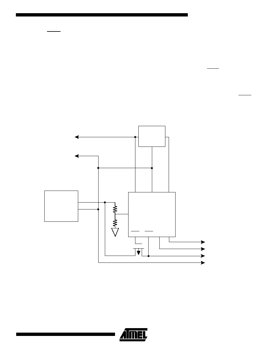
Block Diagram
Note:
This document assumes that the reader is familiar with the Universal Serial Bus and therefore only describes the unique fea-
tures of the AT43312 chip. For detailed information about the USB and its operation, the reader should refer to the Universal
Serial Bus Specification Version 1.0, January 19, 1996.
Figure 1. Device Pins
HUB
CONTROLLER
SERIAL INTERFACE
ENGINE
HUB
REPEATER
ENDPOINT 0
ENDPOINT 1
PORT1
PORT2
PORT3
PORT4
Upstream port
Port0
To downstream
devices
OSC
&
PLL
SERIAL
INTERFACE
ENGINE
HUB
REPEATER
HUB
CONTROLLER
BUS/SELF
DP0
DM0
LFT
OSC1
PSC2
DP4
DM4
OVL4
PWR4
STAT4
PORT4
DP3
DM3
OVL3
PWR3
STAT3
PORT3
DP2
DM2
OVL2
PWR2
STAT2
PORT2
DP1
DM1
OVL1
PWR1
STAT1
PORT4
VREF
VCC3
VCC5
VCCA
GND

AT43312
3
Note:
Signals with a # are active low.
Pin Description
Pin Description
Pin Type
Description
OSC1
I
Oscillator Input. Input to the inverting 6 MHz oscillator amplifier.
OSC2
O
Oscillator Output. Output of the inverting oscillator amplifier.
LFT
I
PLL Filter. For proper operation of the PLL, this pin should be connected through a 2.2 nF capacitor in
parallel with a 100
resistor in series with a 10 nF capacitor to ground (GND)
BUS/SELF
I
Hub Power Mode. Input signal that sets the bus or self-powered mode operation. A high on this pin
enables the bus-powered mode, a low the self-powered mode.
VREF
I
Reference Voltage. This is an input pin that should be connected to an external voltage source. V
REF
is used internally as the reference voltage by the overload protection circuit to decide whether there is
a problem with a port's power.
DP0
B
Upstream Plus USB I/O. This pin should be connected to V
CC
through an external 1.5 K
pullup
resistor. DP0 and DM0 form the differential signal pin pairs connected to the Host Controller or an
upstream Hub.
DM0
B
Upstream Minus USB I/O
DP[1:4]
B
Port Plus USB I/O. This pin should be connected to V
SS
through an external 15 K
resistor. DP[1:4]
and DM[1:4] are the differential signal pin pairs to connect downstream USB devices.
DM[1:4]
B
Port Minus USB I/O. This pin should be connected to V
SS
through an external 15 K
resistor.
OVC[1:4]
I
Overcurrent. This is the input signal used to indicate to the AT43312 that an overcurrent is detected at
the port. If OVC is asserted, AT43312 will assert the PWRx pin and report the status to the USB Host.
PWR[1:4]
OD
Power Switch. This is an output signal used to enable or disable the external voltage regulator
supplying power to a port. PWRx is de-asserted when a power supply problem is detected at OVCx.
STAT[1:4]
O
Connect Status. This is an output pin indicating that a port is properly connected. STATx is asserted
when the port is enabled.
V
CC3
V
3.3V Power Supply
V
CC5
V
5V Power Supply
V
CCA
V
5V Analog Power Supply
GND
V
Ground

AT43312
4
Functional Description
The Atmel AT43312 is a USB hub controller for use in a
standalone hub, as well as an add-on hub for an existing
non-USB peripheral such as a PC display monitor or key-
board. In addition to supporting the standard USB hub
functionality, the AT43312 has additional features to
enhance the user friendliness of the hub.
USB Ports
The AT43312's downstream ports are standard USB ports.
That is, their functionality complies to the USB specification
and any USB compliant device can be attached to these
ports without any other circuitry or modification. Each port
has a port connectivity status pin.
Dp And Dm Configuration
To match the full-speed cable impedance, 27
series
resistors must be connected between each port's DM and
DP pins to their corresponding USB connector. In addition,
15 K
pull-down resistors are required at each down-
stream port's DM and DP pins. Port0 is a full-speed port
and requires a 1.5 K
pull-up resistor to the 3.3V power
supply. This power supply must be derived from the bus
supplied power.
Port Status Pin
The STATx pins are signals that are not required by the
USB specification. Their function is to allow the hub to pro-
vide feedback to the user whenever a device is properly
connected to the port. A LED and series resistor connected
to STAx can be used to provide a visual feedback.
The default state of STATx is inactive. After a port is
enabled, AT43312 will assert the port's STATx. Any condi-
tion that causes the port to be disabled inactivates STATx.
Hub Repeater
The Hub Repeater is responsible for port connectivity setup
and tear-down. It also supports exception handling such as
bus fault detection and recovery, and connect/disconnect
detection. Port0 is the root port and is connected to the root
hub or an upstream hub. When a packet is received at
Port0, the AT43312 propagates it to all of the enabled
downstream ports. Conversely, a packet from a down-
stream port is transmitted from Port0.
The AT43312 supports downstream port data signaling at
both 1.5 Mb/s and 12 Mb/s. Devices attached to the down-
stream ports are determined to be either full-speed or low-
speed depending on which data line (DP or DM) is pulled
high. If a port is enumerated as low speed, its output buff-
ers operate at a slew rate of 75-300 ns, and the AT43312
will not propagate any traffic to that port unless it is pref-
aced with a preamble PID. Low-speed data following the
preamble PID is propagated to both low and full-speed
devices. The AT43312 will enable low-speed drivers within
four full-speed bit times of the last bit of a preamble PID,
and will disable them at the end of an EOP. Packets out of
Port0 are always transmitted using the full-speed drivers.
All the AT43312 ports independently drive and monitor
their DP and DM pins so that they are able to detect and
generate the `J', `K', and SE0 bus signaling states. Each
hub port has single-ended and differential receivers on its
DP and DM lines. The ports I/O buffers comply to the volt-
age levels and drive requirements as specified in the USB
Specifications Rev 1.0.
The Hub Repeater implements a frame timer which is timed
by the 12MHz USB clock and gets reset every time a SOF
token is received from the Host.
Serial Interface Engine
The Serial Interface Engine handles the USB communica-
tion protocol. It performs the USB clock/data separation,
the NRZI data encoding/decoding, bit stuffing, CRC gener-
ation and checking, USB packet ID decoding and genera-
tion, and data serialization and de-serialization. The on-
chip phase locked loop generates the high-frequency clock
for the clock/data separation circuit.
Power Management
A hub is a high-powered device and is allowed to draw up
to 500 mA of current from the host or upstream hub. The
AT43312 chip itself and its external hub circuitry consume
less than 100 mA. The AT43312's power management
logic work with external devices to detect overcurrent and
control power to the ports.
Overcurrent sensing is on a per port basis and is achieved
through the OVCx pins. Each of the OVCx pin is the plus
input of an analog comparator whose other input is con-
nected to a reference voltage source, V
REF
which is com-
mon to all four ports. Whenever the voltage at OVCx is less
than V
REF
, the AT43312 treats it as an overcurrent condi-
tion. This could be caused by an overload, or even a short
c i rcu it , a n d c a u s e s th e A T 4 3 3 1 2 t o s e t t h e p o r t ' s
P O R T _ O V E R _ C U R R E N T s t a t u s b i t a n d i t s
C_PORT_OVER_CURRENT status change bit. At the
same time, power to the offending port is shut off.
An external device is needed to perform the actual switch-
ing of the ports' power under control of the AT43312. The
signal to control the external switches are the PWRx pins
which are open drain signals and require external pull-up
resistors of 10 K
. Any type of suitable switch or device is
acceptable. However, it should have a low-voltage drop
across it even when the port absorbs full power. In its sim-
plest form, this switch can be a P-channel MOSFET. The
advantages of using a MOSFET switch is its very low volt-
age drop and low cost.
Each one of the AT43312's port has its own power control
p i n w h i c h i s a s s e r t e d o n l y w h e n a
Set_Port_Feature[PORT-POWER] request is received
AT43312
5
from the host. PWRx is de-asserted under the following
conditions:
1.
Power up
2.
Reset and initialization
3.
Overcurrent condition
Self-powered Mode
In the self-powered mode, power to the downstream ports
must be supplied by an external power supply. This power
supply must be capable of supplying 500 mA per port.
The USB specifications require that the voltage drop at the
power switch, and board traces be no more than 100 mV. A
good conservative maximum drop at the power switch itself
should be no more than 750 mV. Careful design and selec-
tion of the power switch and PC board layout is required to
meet the specifications. When using a MOSFET switch, its
resistance must be 140 M
or less, under worst case con-
ditions. A suitable MOSFET switch for an AT43312 based
hub is a P-channel enhancement mode MOSFET. The
input of the PMOS switch is connected to the local 5V
power supply while the output is connected to the port
power line, as well as the port's OVCx pin. An overcurrent
condition increases the voltage drop across the MOSFET.
If this voltage drops to less than the voltage at V
REF
, the
AT43312 voltage reference pin, the AT43312 interpretes
this as an overcurrent condition. The AT43312 removes the
power from that port by de-activating the port's PWRx pin
and reports the condition to the Host.
Figure 2. Self-Powered Hub Power Supply
Bus-powered Mode
In the bus-powered mode, all the power for the hub itself as
well as the downstream ports are supplied by the root hub
or upstream hub through the USB. Only 100 mA is avail-
able for each of the hub's downstream devices and there-
fore only low power devices are supported.
The power switch and overcurrent protection work exactly
like the self-powered mode, except that the allowable
switch resistance is higher: 700 M
or less under the
worst-case condition.
The diagrams of Figures 2 and 3 show examples of the
power supply and management connections for a typical
AT43312 port in the self-powered mode and bus-powered
mode.
R1
R2
VCC5
GND
VCC3
PWR
OVC
DM
DP
VREF
3V REG
IN
OUT
GND
BUS_POWER
GND
POWER SUPPLY
5V OUT
GND
AT43312
MOSFET P
DP
DM
PORT_POWER
GND
To
downstream
device