 | –≠–ª–µ–∫—Ç—Ä–æ–Ω–Ω—ã–π –∫–æ–º–ø–æ–Ω–µ–Ω—Ç: AT45DB642 | –°–∫–∞—á–∞—Ç—å:  PDF PDF  ZIP ZIP |

1
Features
∑
Single 2.7V - 3.6V Supply
∑
Dual-interface Architecture
≠ Dedicated Serial Interface (SPI Modes 0 and 3 Compatible)
≠ Dedicated Parallel I/O Interface (Optional Use)
∑
Page Program Operation
≠ Single Cycle Reprogram (Erase and Program)
≠ 8192 Pages (1056 Bytes/Page) Main Memory
∑
Supports Page and Block Erase Operations
∑
Two 1056-byte SRAM Data Buffers ≠ Allows Receiving of Data
while Reprogramming the Flash Array
∑
Continuous Read Capability through Entire Array
≠ Ideal for Code Shadowing Applications
∑
Low-power Dissipation
≠ 4 mA Active Read Current Typical
≠ 2 µA CMOS Standby Current Typical
∑
20 MHz Maximum Clock Frequency ≠ Serial Interface
∑
5 MHz Maximum Clock Frequency ≠ Parallel Interface
∑
Hardware Data Protection
∑
Commercial and Industrial Temperature Ranges
Description
The AT45DB642 is a 2.7-volt only, dual-interface Flash memory ideally suited for a
wide variety of digital voice-, image-, program code- and data-storage applications. The
dual-interface of the AT45DB642 allows a dedicated serial interface to be connected to a
DSP and a dedicated parallel interface to be connected to a microcontroller or vice versa.
64-megabit
2.7-volt Only
Dual-interface
DataFlash
Æ
AT45DB642
Pin Configurations
Pin Name
Function
CS
Chip Select
SCK/CLK
Serial Clock/Clock
SI
Serial Input
SO
Serial Output
I/O7 - I/O0
Parallel Input/Output
WP
Hardware Page Write Protect Pin
RESET
Chip Reset
RDY/BUSY
Ready/Busy
SER/PAR
Serial/Parallel Interface Control
DataFlash Card
(1)
Note:
1. See AT45DCB008 Datasheet.
7 6 5 4 3 2 1
TSOP Top View
Type 1
Note:
*Optional Use ≠ See pin description
text for connection information.
1
2
3
4
5
6
7
8
9
10
11
12
13
14
15
16
17
18
19
20
40
39
38
37
36
35
34
33
32
31
30
29
28
27
26
25
24
23
22
21
NC
NC
RDY/BUSY
RESET
WP
NC
NC
NC
VCC
GND
NC
NC
NC
NC
CS
SCK/CLK
SI*
SO*
NC
NC
NC
NC
NC
NC
NC
I/O7*
I/O6*
I/O5*
I/O4*
VCCP*
GNDP*
I/O3*
I/O2*
I/O1*
I/O0*
SER/PAR*
NC
NC
NC
NC
Rev. 1638F≠DFLSH≠09/02
2
AT45DB642
1638F≠DFLSH≠09/02
However, the use of either interface is purely optional. Its 69,206,016 bits of memory are orga-
nized as 8192 pages of 1056 bytes each. In addition to the main memory, the AT45DB642
also contains two SRAM data buffers of 1056 bytes each. The buffers allow receiving of data
while a page in the main memory is being reprogrammed, as well as reading or writing a con-
tinuous data stream. EEPROM emulation (bit or byte alterability) is easily handled with a self-
contained three step Read-Modify-Write operation. Unlike conventional Flash memories that
are accessed randomly with multiple address lines and a parallel interface, the DataFlash
Æ
uses either a serial interface or a parallel interface to sequentially access its data. The simple
sequential access facilitates hardware layout, increases system reliability, minimizes switching
noise, and reduces package size and active pin count. DataFlash supports SPI mode 0 and
mode 3. The device is optimized for use in many commercial and industrial applications where
high-density, low-pin count, low-voltage, and low-power are essential. The device operates at
clock frequencies up to 20 MHz with a typical active read current consumption of 4 mA.
To allow for simple in-system reprogrammability, the AT45DB642 does not require high input
voltages for programming. The device operates from a single power supply, 2.7V to 3.6V, for
both the program and read operations. The AT45DB642 is enabled through the chip select pin
(CS) and accessed via a three-wire interface consisting of the Serial Input (SI), Serial Output
(SO), and the Serial Clock (SCK), or a parallel interface consisting of the parallel input/output
pins (I/O7 - I/O0) and the clock pin (CLK). The SCK and CLK pins are shared and provide the
same clocking input to the DataFlash.
All programming cycles are self-timed, and no separate erase cycle is required before
programming.
When the device is shipped from Atmel, the most significant page of the memory array may
not be erased. In other words, the contents of the last page may not be filled with FFH.
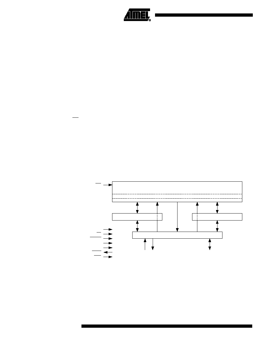
Block Diagram
Memory Array
To provide optimal flexibility, the memory array of the AT45DB642 is divided into three levels
of granularity comprising of sectors, blocks and pages. The "Memory Architecture Diagram"
illustrates the breakdown of each level and details the number of pages per sector and block.
All program operations to the DataFlash occur on a page-by-page basis; however, the optional
erase operations can be performed at the block or page level.
FLASH MEMORY ARRAY
PAGE (1056 BYTES)
BUFFER 2 (1056 BYTES)
BUFFER 1 (1056 BYTES)
I/O INTERFACE
SCK/CLK
CS
RESET
VCC
GND
RDY/BUSY
SER/PAR
WP
SO
SI
I/O7 - I/O0

3
AT45DB642
1638F≠DFLSH≠09/02
Memory Architecture Diagram
Device
Operation
The device operation is controlled by instructions from the host processor. The list of instruc-
tions and their associated opcodes are contained in Tables 1 through 4. A valid instruction
starts with the falling edge of CS followed by the appropriate 8-bit opcode and the desired
buffer or main memory address location. While the CS pin is low, toggling the SCK/CLK pin
controls the loading of the opcode and the desired buffer or main memory address location
through either the SI (serial input) pin or the parallel input pins (I/O7 - I/O0). All instructions,
addresses, and data are transferred with the most significant bit (MSB) first.
Buffer addressing is referenced in the datasheet using the terminology BFA10 - BFA0 to
denote the 11 address bits required to designate a byte address within a buffer. Main memory
addressing is referenced using the terminology PA12 - PA0 and BA10 - BA0, where PA12 -
PA0 denotes the 13 address bits required to designate a page address and BA10 - BA0
denotes the 11 address bits required to designate a byte address within the page.
Read Commands
By specifying the appropriate opcode, data can be read from the main memory or from either
one of the two SRAM data buffers. The DataFlash supports two categories of read modes in
relation to the SCK/CLK signal. The differences between the modes are in respect to the inac-
tive state of the SCK/CLK signal as well as which clock cycle data will begin to be output. The
two categories, which are comprised of four modes total, are defined as Inactive Clock Polarity
Low or Inactive Clock Polarity High and SPI Mode 0 or SPI Mode 3. A separate opcode (refer
to Table 1 for a complete list) is used to select which category will be used for reading. Please
refer to the "Detailed Bit-level Read Timing" diagrams in this datasheet for details on the clock
cycle sequences for each mode.
SECTOR 0 = 8 Pages
8448 bytes (8K + 256)
SECTOR 1 = 248 Pages
261,888 bytes (248K + 7936)
Block = 8448 bytes
(8K + 256)
8 Pages
SECTOR 0
SECTOR 1
Page = 1056 bytes
(1K + 32)
PAGE 0
PAGE 1
PAGE 6
PAGE 7
PAGE 8
PAGE 9
PAGE 8190
PAGE 8191
BLOCK 0
PAGE 14
PAGE 15
PAGE 16
PAGE 17
PAGE 18
PAGE 8189
BLOCK 1
SECTOR ARCHITECTURE
BLOCK ARCHITECTURE
PAGE ARCHITECTURE
BLOCK 0
BLOCK 1
BLOCK 30
BLOCK 31
BLOCK 32
BLOCK 33
BLOCK 1022
BLOCK 1023
BLOCK 62
BLOCK 63
BLOCK 64
BLOCK 65
SECTOR 2
SECTOR 32 = 256 Pages
270,336 bytes (256K + 8K)
BLOCK 2
SECTOR 2 = 256 Pages
270,336 bytes (256K + 8K)
SECTOR 31 = 256 Pages
270,336 bytes (256K + 8K)
SECTOR 3 = 256 Pages
270,336 bytes (256K + 8K)

4
AT45DB642
1638F≠DFLSH≠09/02
CONTINUOUS ARRAY READ: By supplying an initial starting address for the main memory
array, the Continuous Array Read command can be utilized to sequentially read a continuous
stream of data from the device by simply providing a clock signal; no additional addressing
information or control signals need to be provided. The DataFlash incorporates an internal
address counter that will automatically increment on every clock cycle, allowing one continu-
ous read operation without the need of additional address sequences. To perform a
continuous read, an opcode of 68H or E8H must be clocked into the device followed by three
address bytes (which comprise the 24-bit page and byte address sequence) and a series of
don't care bytes (four don't care bytes if using the serial interface or 60 don't care bytes if
using the parallel interface). The first 13 bits (PA12 - PA0) of the 24-bit (three byte) address
sequence specify which page of the main memory array to read, and the last 11 bits (BA10 -
BA0) of the 24-bit address sequence specify the starting byte address within the page. The
four or 60 don't care bytes that follow the three address bytes are needed to initialize the read
operation. Following the don't care bytes, additional clock pulses on the SCK/CLK pin will
result in data being output on either the SO (serial output) pin or the parallel output pins (I/O7-
I/O0).
The CS pin must remain low during the loading of the opcode, the address bytes, the don't
care bytes, and the reading of data. When the end of a page in main memory is reached dur-
ing a Continuous Array Read, the device will continue reading at the beginning of the next
page with no delays incurred during the page boundary crossover (the crossover from the end
of one page to the beginning of the next page). When the last bit (or byte if using the parallel
interface mode) in the main memory array has been read, the device will continue reading
back at the beginning of the first page of memory. As with crossing over page boundaries, no
delays will be incurred when wrapping around from the end of the array to the beginning of the
array.
A low-to-high transition on the CS pin will terminate the read operation and tri-state the output
pins (SO or I/O7-I/O0). The maximum SCK/CLK frequency allowable for the Continuous Array
Read is defined by the f
CAR
specification. The Continuous Array Read bypasses both data
buffers and leaves the contents of the buffers unchanged.
BURST ARRAY READ WITH SYNCHRONOUS DELAY: The Burst Array Read with Synchro-
nous Delay functions very similarly to the Continuous Array Read operation but allows much
higher read throughputs by utilizing faster clock frequencies. It incorporates a synchronous
delay (through the use of don't care clock cycles) when crossing over page boundaries. To
perform a Burst Array Read with Synchronous Delay, an opcode of 69H or E9H must be
clocked into the device followed by three address bytes (which comprise the 24-bit page and
byte address sequence) and a series of don't care bytes (four don't care bytes if using the
serial interface or 60 don't care bytes if using the parallel interface). The first 13 bits (PA12-
PA0) of the 24-bit (three byte) address sequence specify which page of the main memory
array to read, and the last 11 bits (BA10-BA0) of the 24-bit address sequence specify the start-
ing byte address within the page. The don't care bytes that follow the three address bytes are
needed to initialize the read operation. Following the don't care bytes, additional clock pulses
on the SCK/CLK pin will result in data being output on either the SO pin or the I/O7-I/O0 pins.

5
AT45DB642
1638F≠DFLSH≠09/02
As with the Continuous Array Read, the CS pin must remain low during the loading of the
opcode, the address bytes, the don't care bytes, and the reading of data. During a Burst Array
Read with Synchronous Delay, when the end of a page in main memory is reached (the last bit
or the last byte of the page has been clocked out), the system must send an additional 32
don't care clock cycles before the first bit (or byte if using the parallel interface mode) of the
next page can be read out. These 32 don't care clock cycles are necessary to allow the device
enough time to cross over the burst read boundary (the crossover from the end of one page to
the beginning of the next page). By utilizing the 32 don't care clock cycles, the system does
not need to delay the SCK/CLK signal to the device which allows synchronous operation when
reading multiple pages of the memory array. Please see the detailed read timing waveforms
for illustrations (beginning on page 21) on which clock cycle data will actually begin to be
output.
When the last bit (or byte in the parallel interface mode) in the main memory array has been
read, the device will continue reading back at the beginning of the first page of memory. The
transition from the last bit (or byte when using the parallel interface) of the array back to the
beginning of the array is also considered a burst read boundary. Therefore, the system must
send 32 don't care clock cycles before the first bit (or byte if using the parallel interface mode)
of the memory array can be read.
A low-to-high transition on the CS pin will terminate the read operation and tri-state the output
pins (SO or I/O7-I/O0). The maximum SCK/CLK frequency allowable for the Burst Array Read
with Synchronous Delay is defined by the f
BARSD
specification. The Burst Array Read with Syn-
chronous Delay bypasses both data buffers and leaves the contents of the buffers unchanged.
MAIN MEMORY PAGE READ: A main memory page read allows the user to read data
directly from any one of the 8192 pages in the main memory, bypassing both of the data buff-
ers and leaving the contents of the buffers unchanged. To start a page read, an opcode of 52H
or D2H must be clocked into the device followed by three address bytes (which comprise the
24-bit page and byte address sequence) and a series of don't care bytes (four don't care bytes
if using the serial interface or 60 don't care bytes if the using parallel interface). The first 13
bits (PA12 - PA0) of the 24-bit (three-byte) address sequence specify the page in main mem-
ory to be read, and the last 11 bits (BA10 - BA0) of the 24-bit address sequence specify the
starting byte address within that page. The four or 60 don't care bytes that follow the three
address bytes are sent to initialize the read operation. Following the don't care bytes, addi-
tional pulses on SCK/CLK result in data being output on either the SO (serial output) pin or the
parallel output pins (I/O7 - I/O0). The CS pin must remain low during the loading of the
opcode, the address bytes, the don't care bytes, and the reading of data. When the end of a
page in main memory is reached, the device will continue reading back at the beginning of the
same page. A low-to-high transition on the CS pin will terminate the read operation and tri-
state the output pins (SO or I/O7 - I/O0).
BUFFER READ: Data can be read from either one of the two buffers, using different opcodes
to specify which buffer to read from. An opcode of 54H or D4H is used to read data from buffer
1, and an opcode of 56H or D6H is used to read data from buffer 2. To perform a buffer read,
the opcode must be clocked into the device followed by three address bytes comprised of 13
don't care bits and 11 buffer address bits (BFA10 - BFA0). Following the three address bytes,
an additional don't care byte must be clocked in to initialize the read operation. Since the
buffer size is 1056 bytes, 11 buffer address bits are required to specify the first byte of data to
be read from the buffer. The CS pin must remain low during the loading of the opcode, the
address bytes, the don't care bytes, and the reading of data. When the end of a buffer is
reached, the device will continue reading back at the beginning of the buffer. A low-to-high
transition on the CS pin will terminate the read operation and tri-state the output pins (SO or
I/O7 - I/O0).