 | –≠–ª–µ–∫—Ç—Ä–æ–Ω–Ω—ã–π –∫–æ–º–ø–æ–Ω–µ–Ω—Ç: AT697E | –°–∫–∞—á–∞—Ç—å:  PDF PDF  ZIP ZIP |
Rev. 4226BS≠AERO≠01/05
1
Note:
This is a summary document. Contact
ATMEL for a complete document.
F
eatures
∑
SPARC V8 High Performance Low-power 32-bit Architecture
≠ LEON2-FT 1.0.13 compliant
≠ 8 Register Windows
∑
Advanced Architecture:
≠ On-chip Amba Bus
≠ 5 Stage Pipeline
≠ 16 kbyte Multi-sets Data Cache
≠ 32 kbyte Multi-sets Instruction Cache
∑
On-chip Peripherals:
≠ Memory Interface
PROM Controller
SRAM Controller
SDRAM Controller
≠ Timers
Two 24-bit Timers
Watchdog Timer
≠ Two 8-bit UARTs
≠ Interrupt Controller with 4 External Programmable Inputs
≠ 32 Parallel I/O Interface
≠ 33MHz PCI Interface Compliant with 2.2 PCI Specification
∑
Integrated 32/64-bit IEEE 754 Floating-point Unit
∑
Fault Tolerance by Design
≠ Full Triple Modular Redundancy (TMR)
≠ EDAC Protection
≠ Parity Protection
∑
Debug and Test Facilities
≠ Debug Support Unit (DSU) for Trace and Debug
≠ IEEE 1149.1 JTAG Interface
≠ Four Hardware Watchpoints
∑
Speed Optimized Code RAM Interface
8, 16 and 40-bit boot-PROM (Flash) Interface Possibilities
∑
Clock: 0MHz up to 100MHz
∑
Core consumption: 1W
∑
Performance: 100 MIPS
∑
Operating range
≠ Voltages
3.3V +/- 0.30V for I/O
1.8V +/- 0.15V for Core
≠ Temperature
-55∞C to 125∞C
∑
Radiation Performance
≠ Total dose radiation capability (parametric & functional): 100Krads (Si) (target)
≠ SEU event rate better than 1 E-5 error/device/day (target)
≠ Latch up immunity better than 70 MeV.cm≤/mg
∑
Package MCGA 349
∑
Mass: 9g
Rad-Hard 32 bit
SPARC V8
Processor
AT697E
Advance
Information
Summary
2
AT697E
4226BS≠AERO≠01/05
Description
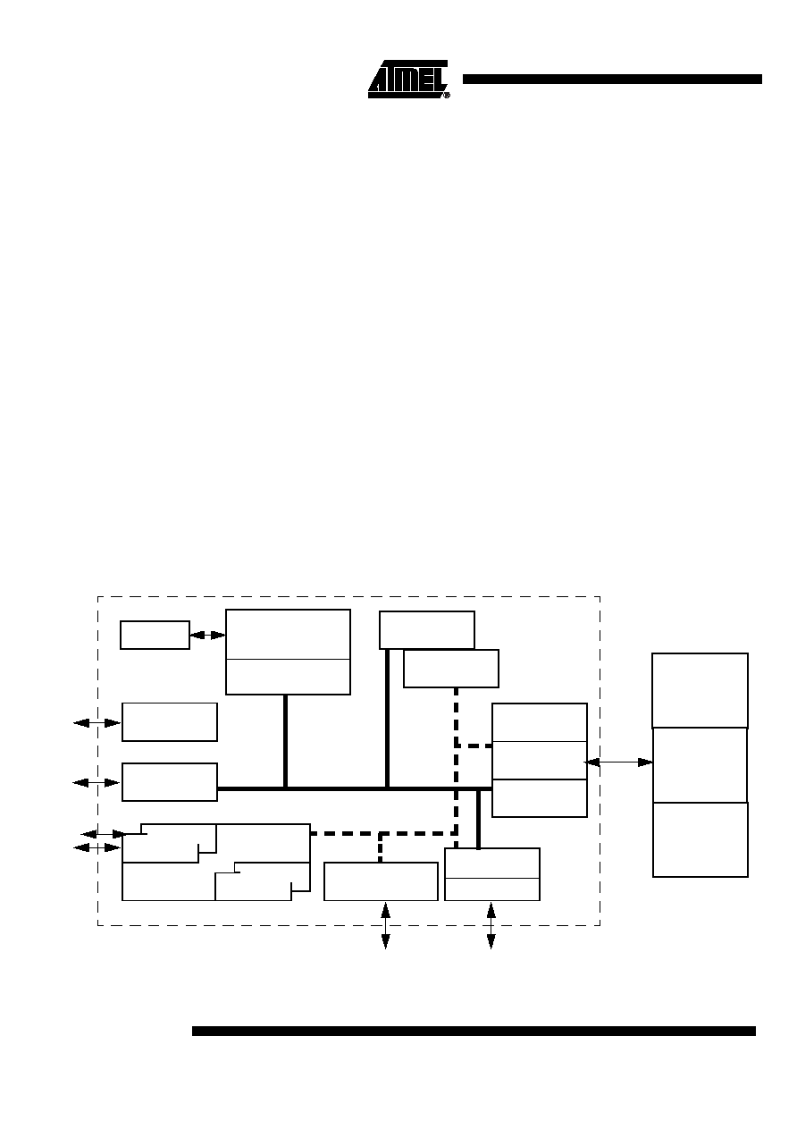
The AT697 is a highly integrated, high-performance 32-bit RISC embedded processor
based on the SPARC V8 architecture. The implementation is based on the European
Space Agency (ESA) LEON2 fault tolerant model. By executing powerful instructions in
a single clock cycle, the AT697 achieves throughputs approaching 1MIPS per MHz,
allowing the system designer to optimize power consumption versus processing speed.
The AT697 is designed to be used as a building block in computers for on-board embed-
ded real-time applications. It brings up-to-date functionality and performance for space
application.
The AT697 only requires memory and application specific peripherals to be added to
form a complete on-board computer.
The AT697 contains an on-chip Integer Unit (IU), a Floating Point Unit (FPU), separate
instruction and data caches, hardware multiplier and divider, interrupt controller, debug
support unit with trace buffer, two 24-bit timers, Parallel and Serial interfaces, a Watch-
dog, a PCI Interface and a flexible Memory Controller. The design is highly testable with
the support of a Debug Support Unit (DSU) and a boundary scan through JTAG
interface.
An idle mode stops the CPU while allowing Timer/Counter, Serial ports and Interrupt
system to continue functioning.
The processor is manufactured using the Atmel 0.18 µm CMOS process. It has been
especially designed for space, by implementing on-chip concurrent transient and per-
manent error detection and correction.
Figure 1. AT697 Block Diagram
Interrupt
Controller
UART B
Timer 1
Timer 2
General Purpose
Interface
Debug Support
Unit
FPU
Integer Unit
(SPARC V8)
I-Cache
AHB/APB
bridge
AHB
Controller
Amba APB
Amba AHB
Watchdog
PCI
Waitstate
Memory
Controller
Controller
EDAC
RxD
TxD
RxD
TxD
GPI bits
PCI bus
Ready
Busy
Add.
...
JTAG
TAP
TDS
TDI
TDO
...
Prom
SRAM
SDRAM
I/O
D-Cache
PCI/AMBA
bridge
UART A

3
AT697E
4226BS≠AERO≠01/05
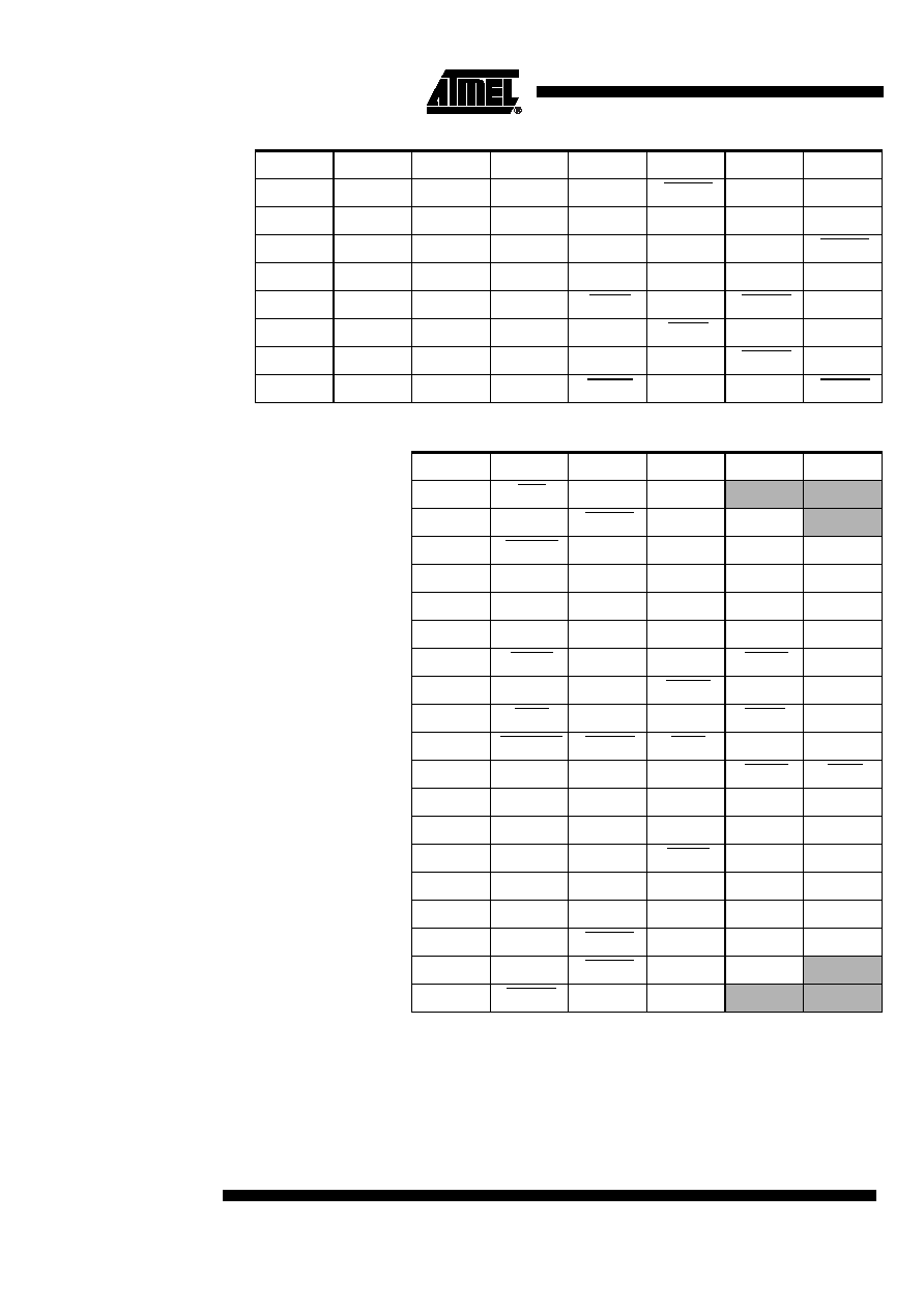
Pin Configuration
Table 1. AT697 pinout
Table 2. AT697 pinout (suite)
A
B
C
D
E
F
G
1
VDD18
VSS18
PIO[6]
PIO[1]
RAMS[1]
2
VSS18
VDD18
PIO[0]
N.C.
PIO[4]
RAMS[2]
3
VDD18
VDD18
VSS18
VCC33
PIO[2]
N.C.
RAMOE[3]
4
VSS18
VDD18
PIO[9]
N.C.
PIO[5]
PIO[3]
RAMS[4]
5
N.C.
N.C.
PIO[11]
N.C.
N.C.
VSS33
RAMOE[1]
6
PIO[13]
PIO[10]
VCC33
Reserved
CB[0]
N.C.
VSS33
7
CB[1]
VSS33
N.C.
PIO[15]
VSS33
PIO[12]
PIO[7]
8
CB[6]
CB[4]
D[2]
VCC33
CB[7]
CB[2]
PIO[8]
9
D[3]
N.C.
D[1]
VSS33
D[6]
VCC33
CB[3]
10
D[8]
D[5]
VCC33
VSS33
Reserved
D[10]
D[4]
11
D[12]
VSS33
VCC33
D[13]
D[7]
D[15]
N.C.
12
D[17]
D[18]
D[11]
VSS33
D[14]
D[16]
D[19]
13
D[21]
D[23]
VCC33
VCC33
VSS33
VSS33
A[1]
14
D[25]
N.C.
D[22]
D[27]
N.C.
VSS33
A[3]
15
D[30]
N.C.
D[26]
D[29]
N.C.
N.C.
A[12]
16
VSS18
VSS18
D[28]
VCC33
N.C.
N.C.
A[6]
17
VDD18
VDD18
VSS18
D[31]
N.C.
A[7]
VSS33
18
VSS18
VDD18
VCC33
A[0]
A[4]
A[8]
19
VDD18
VSS18
A[2]
VSS33
A[9]
H
J
K
L
M
N
P
1
RAMOE[0]
VSS33
READ
DSUACT
BEXC
VCC33
SDWE
2
RAMOE[2]
ROMS[1]
TCK
DSURX
SDCLK
VSS33
PCI_CLK
3
VCC33
ROMS[0]
TDI
DSUTX
DSUBRE
SDDQM[1]
VSS33
4
RAMOE[4]
RWE[0]
TDO
DSUEN
SDDQM[2]
N.C.
SDCS[0]
5
RWE[1]
WRITE
VSS33
TMS
N.C.
SDDQM[3]
SDCAS
6
RWE[3]
RWE[2]
IOS
VSS33
VSS33
GNT
A/D[24]
7
RAMS[0]
N.C.
TRST
SDDQM[0]
VSS33
VCC33
A/D[30]
8
RAMS[3]
VCC33
OE
BRDY
VCC33
A/D[21]
A/D[18]
9
CB[5]
PIO[14]
VSS33
SDRAS
A/D[22]
A/D[16]
A/D[17]
10
D[9]
D[0]
N.C.
A/D[14]
VSS33
PERR
IRDY
11
D[20]
A[5]
A[16]
N.C.
A/D[12]
A/D[9]
A/D[15]
4
AT697E
4226BS≠AERO≠01/05
Table 3. AT697 pinout (suite 2)
Notes:
1. `Reserved' pins shall not be driven to any voltage
2. N.C. refers to unconnected pins
12
D[24]
A[14]
A[26]
VDD_PLL
AGNT[3]
A/D[1]
A/D[8]
13
N.C.
VCC33
A[21]
N.C.
N.C.
VSS33
A/D[5]
14
A[10]
VCC33
A[27]
LOCK
SKEW[1]
A/D[0]
AGNT[1]
15
N.C.
VSS33
VCC33
A[24]
Reserved
BYPASS
CLK
16
A[11]
VSS33
A[23]
RESET
LFT
AREQ[2]
VSS33
17
A[19]
A[17]
VSS33
VCC33
WDOG
N.C.
VSS33
18
A[13]
A[18]
A[22]
VSS33
VSS_PLL
AREQ[3]
N.C.
19
A[15]
A[20]
A[25]
ERROR
SKEW[0]
VCC33
AREQ[1]
H
J
K
L
M
N
P
R
T
U
V
W
1
REQ
VSS18
VDD18
2
N.C.
SDCS[1]
VDD18
VSS18
3
PCI_RST
A/D[31]
VSS18
VDD18
VDD18
4
N.C.
A/D[29]
VCC33
VSS18
VSS18
5
N.C.
N.C.
A/D[26]
N.C.
A/D[28]
6
N.C.
A/D[27]
IDSEL
VSS33
A/D[25]
7
SYSEN
VSS33
VCC33
C/BE[3]
A/D[23]
8
VSS33
VSS33
FRAME
A/D[20]
A/D[19]
9
TRDY
VCC33
N.C.
C/BE[2]
VSS33
10
PCI_LOCK
DEVSEL
STOP
VCC33
VCC33
11
VSS33
VCC33
VSS33
C/BE[1]
SERR
12
N.C.
A/D[11]
PAR
VSS33
A/D[13]
13
VCC33
A/D[7]
A/D[10]
VSS33
VSS33
14
VCC33
VSS33
C/BE[0]
A/D[4]
A/D[6]
15
N.C.
A/D[2]
VCC33
N.C.
A/D[3]
16
N.C.
VCC33
N.C.
VDD18
VSS18
17
VCC33
AGNT[0]
VSS18
VDD18
VDD18
18
N.C.
AGNT[2]
VDD18
VSS18
19
AREQ[0]
VSS18
VDD18

5
AT697E
4226BS≠AERO≠01/05
Pin Description
IU and FPU Signals
A[27:0] - Address bus (output)
A[27:0] bus carries the addresses during accesses on the memory. When no access is
performed to external memory, the address of the last access is driven.
D[31:0] - Data bus (bi-directional)
D[31:0] bus carries the data during transfers on the memory. The processor only drives
the bus during write cycles. During accesses to 8-bit areas, only D[31:24] are used.
CB[7:0] - Check bits (bi-directional)
CB[6:0] bus carries the EDAC checkbits during memory accesses. CB[7]
(1)
takes the
value of tcb[7] in the error control register. Processor only drives CB[7:0] during write
cycles to areas programmed to be EDAC protected.
Note:
1. CB[7] is implemented to enable programming of flash memories. When only 7 bits
are useful for EDAC protection, 8 are needed for programming.
Memory Interface Signals
General management
OE* - Output enable (output)
This active low output is asserted during read cycles on the memory bus
BRDY* - Bus ready (input)
This active low input indicates that the access to a memory mapped I/O area can be ter-
minated on the next rising clock edge.
READ - Read cycle (output)
This active high output is asserted during read cycles on the memory bus.
WRITE* - Write enable (output)
This active low output provides a write strobe during write cycles on the memory bus.
PROM
ROMS*[1:0] - PROM chip-select (output)
These active low outputs provide the chip-select signal for the PROM area. ROMSN[0]
is asserted when the lower half of the PROM area is accessed (0 - 0x10000000), while
ROMSN[1] is asserted for the upper half.
SRAM
RAMOE*[4:0] - RAM output enable (output)
These active low signals provide an individual output enable for each RAM bank.
RAMS*[4:0] - RAM chip-select (output)
These active low outputs provide the chip-select signals for each RAM bank.
RWEN [3:0] - RAM write enable (output)
These active low outputs provide individual write strobes for each byte. RWEN[0] con-
trols D[31:24], RWEN[1] controls D[23:16], etc.
I/O
IOS* - I/O select (output)
This active low output is the chip-select signal for the memory mapped I/O area.