 | –≠–ª–µ–∫—Ç—Ä–æ–Ω–Ω—ã–π –∫–æ–º–ø–æ–Ω–µ–Ω—Ç: AT71200 | –°–∫–∞—á–∞—Ç—å:  PDF PDF  ZIP ZIP |

1
Features
∑
Full-field Image Sensor 3500 x 2300 Pixels
∑
Pixel 10 µm x 10 µm Photo-MOS
∑
Image Zone: 35 mm x 23 mm
∑
Additional Full-frame Operating Mode: 2627 x 2300 pixels of 10 µm x 10 µm (3 zones)
∑
Frame Readout Through One, Two or Four Outputs
∑
Built-in Region of Interest (ROI) Selection
∑
Data Rates Up to 4 x 25 MHz (Compatibility with 10 Frames/Seconds)
∑
High Dynamic Range (Up to 3000), at Room Temperature and at 25 MHz Frequency
∑
Very Low Dark Current (MPP Mode)
∑
Bayer Standard Color Mosaic
∑
Flexibility and Performance Make Device Suitable for Digital Photography, Graphic
Arts, Medical and Industrial Applications
Description
Atmel's AT71200M is a progressive scan sensor based on charge-coupled device
(CCD) technology. It can be used in a wide range of applications thanks to operating
mode flexibility, very high definition and high dynamic range.
The nominal photosensitive area is made up of 2300 x 3500 useful pixels and is split
into four independent zones that are driven separately by four independant four-phase
clocksets. Thus the sensor can be used in up to 12 main modes.
The large format and high definition make the device suitable for any application
requiring precision and accuracy.
The Bayer standard RGB color mosaic has been specially designed for colorimetric
applications and the three colors balanced for a 3800K standard illuminant.
Two serial registers and four independent output amplifiers offer a high-frequency
functionality of up to 10 frames per second and a 12-bit dynamic range.
8M-pixel Color
Image Sensor
AT71200M
Rev. 2133A≠IMAGE≠02/03

2
AT71200M
2133A≠IMAGE≠02/03
Pinout
Figure 1. AT71200M Pinout ≠ Top View
19
18
17
16
15
14
6
5
4
3
2
1
Register A
Zone A
Zone B
Zone C
Zone D
Register B
VOS3
VOS4
VOS1
VOS2
P
N
M
L
K
J
H
G
F
E
D
C
B
A
VDD1
VS1
VGS1
S1
LB4
LB1
VSS
VSS
LB5
LB8
S2
VGS2
VS2
VDD2
VOS1 VDR1
VGL1
R1
LB3
LB2
VSS
LB7
LB6
R2
VGL2
VDR2 VOS2
VSS
VSS
VSS
VSS
VSS1
VSS
VSS
VSS
VSS
VSS
VSS
VSS
VDEB
VFCB
TB
FCB
PD2
PD3
PC3
PC2
PC4
PC1
PD1
PD4
PB1
PB2
PA2
PA1
PB4
PB3
PA3
PA4
VDD3
VS3
VGS3
S3
LA8
LA5
LA1
LA4
S4
VDD4
VS4
VGS4
VOS3 VDR3
VGL3
R3
LA6
LA7
R4
LA3
LA2
VOS4
VDR4
VGL4
VDEA
FCA
TA
VSS1
VFCA

3
AT71200M
2133A≠IMAGE≠02/03
Table 1. AT71200M Pinout
Signal Name
Pin Number
Function
LB[1:8]
F1, F2, G2, E1, J1, J2, H2, K1
B readout register clocks
LA[1:8]
J19, J18, H18, K19, F19, F18,
G18, E19
A readout register clocks
S[1:4]
D1, L1, D19, L19
Summing clocks of the outputs 1, 2, 3 and 4
VGL[1:4]
C2, M2, C18, M18
Readout gate bias of the outputs 1, 2, 3 and 4
VGS[1:4]
C1, M1, C19, M19
Output gate bias of the outputs 1, 2, 3 and 4
VOS[1:4]
A2, P2, A18, P18
Output video signals 1, 2, 3 and 4
VDD[1:4]
A1, P1, A19, P19
Output amplifier drain supplies of the outputs 1, 2, 3 and 4
VS[1:4]
B1, N1, B19, N19
Output amplifier source biases of the outputs 1, 2, 3 and 4
R[1:4]
D2, L2, D18, L18
Reset clocks of the outputs 1, 2, 3 and 4
VDR[1:4]
B2, N2, B18, N18
Reset bias of the outputs 1, 2, 3 and 4
PA[1:4]
P14, N14, N15, P15
A image zone clocks
PB[1:4]
A14, B14, B15, A15
B image zone clocks
PC[1:4]
P6, P5, N5, N6
C image zone clocks
PD[1:4]
A6, A5, B5, B6
D image zone clocks
TA,
TB
B16, N4
Transfer gates from the image zone to the readout registers A
and B respectively
VDEA, VDEB
A17, P3
Shield drains
VFCA, VFCB
P16, A4
Region of interest drains
FCA,
FCB
A16, P4
Region of interest clocks
VSS
A3, B3, B4, E2, G1, H1, K2, M3,
B17, E18, G19, H19, K18, N16,
N17, P17
Substrate bias
4
AT71200M
2133A≠IMAGE≠02/03
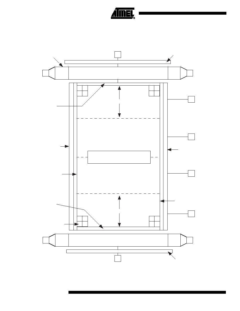
Block Diagram
Figure 2. AT71200M Block Diagram ≠ Top View
Uni- or Bi-directional Readout Register A
873 lines - Zone A
877 lines - Zone B
Full-field Image Sensor
3500 x 2300 active pixels
877 lines - Zone C
873 lines - Zone D
Uni- or Bi-directional Readout Register B
LAi
(i = 1 to 8)
2-phase horizontal clocks
12 pre-scan elements
V
OS3
12
4 dummy lines
(photosensitive)
16 dark references
(100% black)
8 insulating columns
(photosensitive)
4 dummy lines
(photosensitive)
V
OS1
12
First useful pixel
on V
OS1
output (Blue)
PAi (i = 1 to 4)
vertical clocks
PCi (i = 1 to 4)
vertical clocks
PBi (i = 1 to 4)
vertical clocks
PDi (i = 1 to 4)
vertical clocks
LBi
(i = 1 to 8)
2-phase horizontal clocks
Fast clear structure
(
FCB
, V
FCB
)
16 dark references
(100% black)
12
12
V
OS2
V
OS4
Fast clear structure
(
FCA
, V
FCA
)
R
G
G
B
R
G
G
B
R
G
G
B
R
G
G
B
8 insulating columns
(photosensitive)

5
AT71200M
2133A≠IMAGE≠02/03
Architectural
Overview
General Parameters
Note:
1. The design allows the full frame to be read through one, two or four outputs.
Vertical Characteristics ≠
Top to Bottom
AT71200M is made up of four zones, A, B, C and D. The configuration of each zone is
shown in Table 3.
Horizontal
Characteristics
Table 4 gives information on the characteristics seen by one output (V
OS1
, V
OS2
, V
OS3
or
V
OS4
) in different readout modes.
Table 2. General Parameters
Parameters
Value
Pixel size
10 µm x 10 µm
Number of useful pixels on one line
2300
Number of useful lines
3500
Number of readout register
2
Number of outputs
4
(1)
MPP technology
yes
Region of interest structures on readout registers
yes
Built-in antiblooming
no
Pixel mode
4 phase
Readout register mode
2 phase
Table 3. Vertical Characteristics
Zone
Configuration
A
4 dummy photosensitive lines
873 active lines, 100% photosensitive
B
877 active lines, 100% photosensitive
C
877 active lines, 100% photosensitive
D
873 active lines, 100% photosensitive
4 dummy photosensitive lines
Table 4. Horizontal Characteristics
Characteristic
Readout Mode
One Output
Two Outputs on Same Register
Pre-scan elements
12
12
Dark references
16
16
Insulating elements
8
8
Useful pixels
2300
1150