1
4317B≠AVR≠02/05
Features
∑
High Performance, Low Power AVR Æ 8-bit Microcontroller
∑
Advanced RISC Architecture
≠ Powerful Instructions - Most Single Clock Cycle Execution
≠ 32 x 8 General Purpose Working Registers
≠ Fully Static Operation
≠ Up to 1 MIPS throughput per MHz
≠ On-chip 2-cycle Multiplier
∑
Data and Non-Volatile Program Memory
≠ 8K Bytes Flash of In-System Programmable Program Memory
∑ Endurance: 10,000 Write/Erase Cycles
≠ Optional Boot Code Section with Independent Lock Bits
In-System Programming by On-chip Boot Program
True Read-While-Write Operation
≠ 512 Bytes of In-System Programmable EEPROM
∑ Endurance: 100,000 Write/Erase Cycles
≠ 512 Bytes Internal SRAM
≠ Programming Lock for Flash Program and EEPROM Data Security
∑
On Chip Debug Interface (debugWIRE)
∑
Peripheral Features
≠ Two or three 12-bit High Speed PSC (Power Stage Controllers) with 4-bit
Resolution Enhancement
∑ Non Overlapping Inverted PWM Output Pins With Flexible Dead-Time
∑ Variable PWM duty Cycle and Frequency
∑ Synchronous Update of all PWM Registers
∑ Auto Stop Function for Event Driven PFC Implementation
∑ Less than 25 Hz Step Width at 150 kHz Output Frequency
∑ PSC2 with four Output Pins and Output Matrix
≠ One 8-bit General purpose Timer/Counter with Separate Prescaler and Capture
Mode
≠ One 16-bit General purpose Timer/Counter with Separate Prescaler, Compare
Mode and Capture Mode
≠ Programmable Serial USART
∑ Standard UART mode
∑ 16/17 bit Biphase Mode for DALI Communications
≠ Master/Slave SPI Serial Interface
≠ 10-bit ADC
∑ Up To 11 Single Ended Channels and 2 Fully Differential ADC Channel Pairs
∑ Programmable Gain (5x, 10x, 20x, 40x on Differential Channels)
∑ Internal Reference Voltage
≠ 10-bit DAC
≠ Two or three Analog Comparator with Resistor-Array to Adjust Comparison
Voltage
≠ 4 External Interrupts
≠ Programmable Watchdog Timer with Separate On-Chip Oscillator
∑
Special Microcontroller Features
≠ Low Power Idle, Noise Reduction, and Power Down Modes
≠ Power On Reset and Programmable Brown Out Detection
≠ Flag Array in Bit-programmable I/O Space (4 bytes)
≠ In-System Programmable via SPI Port
≠ Internal Calibrated RC Oscillator ( 8 MHz)
≠ On-chip PLL for fast PWM ( 32 MHz, 64 MHz) and CPU (16 MHz)
∑
Operating Voltage: 2.7V - 5.5V
∑
Extended Operating Temperature:
≠ -40∞C to +105∞
(full analog from -40 to 90∞C)
8-bit
Microcontroller
with 8K Bytes
In-System
Programmable
Flash
AT90PWM2
AT90PWM3
Preliminary
3
AT90PWM2/3
4317B≠AVR≠02/05
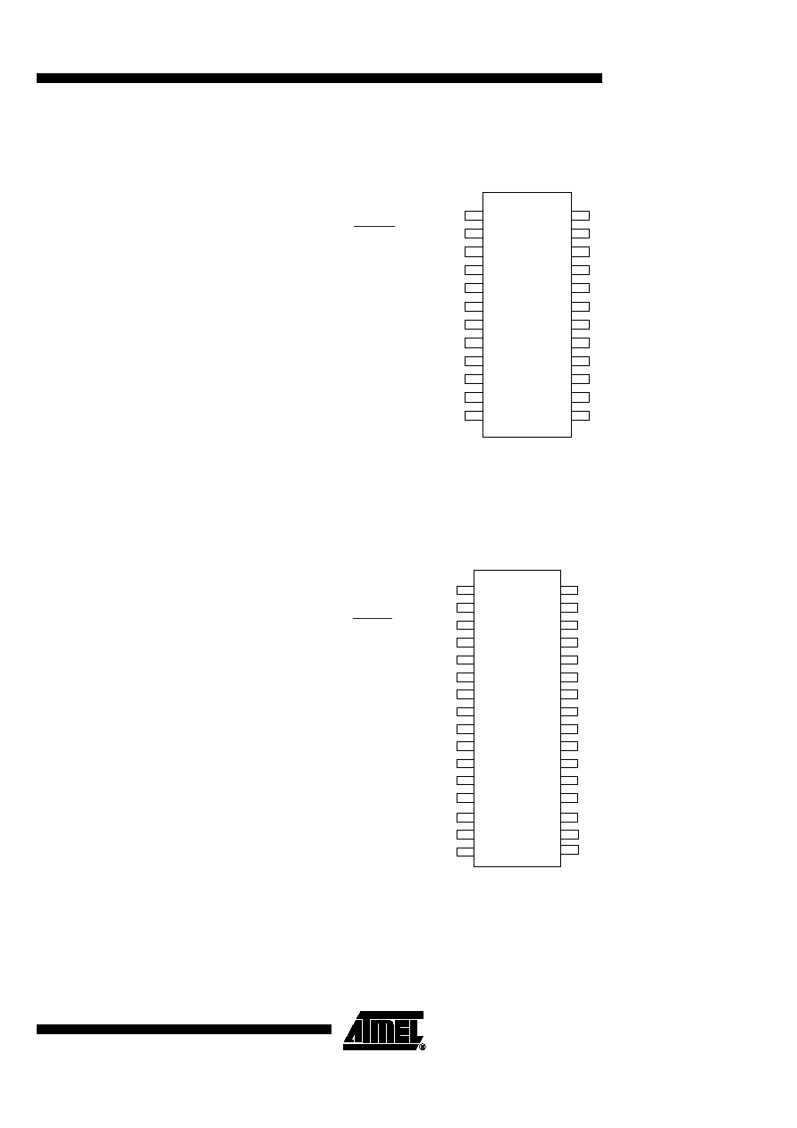
Pin Configurations
Figure 1. SOIC 24-pin Package
Figure 2. SOIC 32-pin Package
AT90PWM2
SOIC24
1
2
3
4
5
6
7
8
9
10
11
12
24
23
22
21
20
19
18
17
16
15
14
13
(PSCOUT00/XCK/SS_A) PD0
(RESET/OCD) PE0
(PSCIN0/CLKO) PD1
(PSCIN2/OC1A/MISO_A) PD2
(TXD/DALI/OC0A/SS/MOSI_A) PD3
VCC
GND
(MISO/PSCOUT20) PB0
(MOSI/PSCOUT21) PB1
(OC0B/XTAL1) PE1
(ADC0/XTAL2) PE2
(ADC1/RXD/DALI/ICP1A/SCK_A) PD4
PB7(ADC4/PSCOUT01/SCK)
PB6 (ADC7/ICP1B)
PB5 (ADC6/INT2)
PB4 (AMP0+)
PB3 (AMP0-)
AREF
AGND
AVCC
PB2 (ADC5/INT1)
PD7 (ACMP0)
PD6 (ADC3/ACMPM/INT0)
PD5 (ADC2/ACMP2)
AT90PWM3
SOIC 32
1
2
3
4
5
6
7
8
9
10
11
12
13
14
15
16
32
31
30
29
28
27
26
25
24
23
22
21
20
19
18
17
(PSCOUT00/XCK/SS_A) PD0
(INT3/PSCOUT10) PC0
(RESET/OCD) PE0
(PSCIN0/CLKO) PD1
(PSCIN2/OC1A/MISO_A) PD2
(TXD/DALI/OC0A/SS/MOSI_A) PD3
(PSCIN1/OC1B) PC1
VCC
GND
(T0/PSCOUT22) PC2
(T1/PSCOUT23) PC3
(MISO/PSCOUT20) PB0
(MOSI/PSCOUT21) PB1
(OC0B/XTAL1) PE1
(ADC0/XTAL2) PE2
(ADC1/RXD/DALI/ICP1A/SCK_A) PD4
PB7(ADC4/PSCOUT01/SCK)
PB6 (ADC7/PSCOUT11/ICP1B)
PB5 (ADC6/INT2)
PC7 (D2A)
PB4 (AMP0+)
PB3 (AMP0-)
PC6 (ADC10/ACMP1)
AREF
AGND
AVCC
PC5 (ADC9/AMP1+)
PC4 (ADC8/AMP1-)
PB2 (ADC5/INT1)
PD7 (ACMP0)
PD6 (ADC3/ACMPM/INT0)
PD5 (ADC2/ACMP2)
5
AT90PWM2/3
4317B≠AVR≠02/05
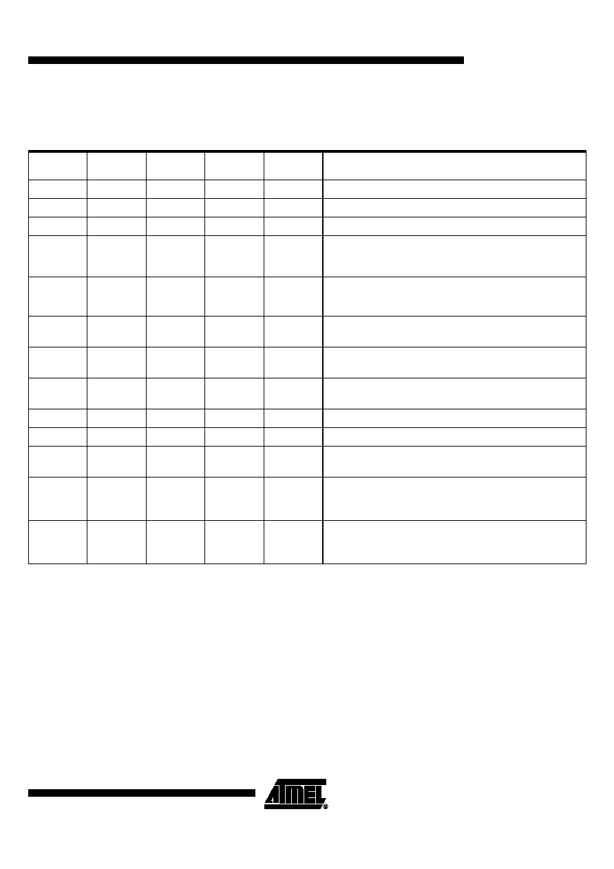
Pin Descriptions
:
Table 1. Pin out description
S024 Pin
Number
SO32 Pin
Number
QFN32 Pin
Number
Mnemonic
Type
Name, Function & Alternate Function
7
9
5
GND
Power
Ground: 0V reference
18
24
20
AGND
Power
Analog Ground: 0V reference for analog part
6
8
4
VCC
power
Power Supply:
17
23
19
AVCC
Power
Analog Power Supply: This is the power supply voltage for analog
part
For a normal use this pin must be connected.
19
25
21
AREF
Power
Analog Reference : reference for analog converter . This is the
reference voltage of the A/D converter. As output, can be used by
external analog
8
12
8
PBO
I/O
MISO (SPI Master In Slave Out)
PSCOUT20 output
9
13
9
PB1
I/O
MOSI (SPI Master Out Slave In)
PSCOUT21 output
16
20
16
PB2
I/O
ADC5 (Analog Input Channel5 )
INT1
20
27
23
PB3
I/O
AMP0- (Analog Differential Amplifier 0 Input Channel )
21
28
24
PB4
I/O
AMP0+ (Analog Differential Amplifier 0 Input Channel )
22
30
26
PB5
I/O
ADC6 (Analog Input Channel 6)
INT 2
23
31
27
PB6
I/O
ADC7 (Analog Input Channel 7)
ICP1B (Timer 1 input capture alternate input)
PSCOUT11 output (see note 1)
24
32
28
PB7
I/O
PSCOUT01 output
ADC4 (Analog Input Channel 4)
SCK (SPI Clock)