Development Tools User Guide
2-1
Section 2
AT89S/AT90S Series Flash
Microcontroller Starter Kit
2.1
Introduction
This manual describes the AT89S/AT90S Series Flash MCU Starter Kit.
The
AVR
Development Board is designed to help new MCU users get quickly
acquainted with the Atmel baseline microcontrollers. The
AVR
Development Board can
also be used to "breadboard" and try new designs before a final PCB is made.
The Starter Kit has the following features:
s
Regulated power supply for both DC and AC voltage sources.
s
8 push buttons for general use.
s
8 LEDs for general use.
s
All
AVR
ports are easy accessible through header connectors.
s
RS-232 level converter for general use.
s
Serial programming of AT90S Series AVR MCUs.
s
Serial programming of AT89S series MCUs.
s
Development board for AT89C/S series MCUs.
Each part of the
AVR
Development Board is described in detail in the following sections.
Note that when the term
AVR
device is used in the text it also covers both the AT90S
series AVR and AT89S series MCU devices, unless specifically noted.
Rev. 1020A-A�01/98
AT89S/AT90S Series Flash Microcontroller Starter Kit
2-2
Development Tools User Guide
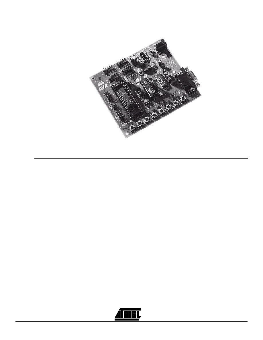
Figure 2-1.
AT89S/AT90S Series Flash Microcontroller Starter Kit.
2.2
The Power
Supply Circuit
The power supply input connector (J140) must be connected to a DC or AC voltage
source. The input circuit is a full bridge rectifier so the polarity of the input voltage does
not really matter, but the general standard on other
AVR
tools without the full bridge rec-
tifier is to connect minus to the center pin. The supplied power cable will get minus on
the center pin if the black/gray lead is connected to minus.
The power supply switch is labeled S140 and is placed close to J140. When a voltage
source is connected to J140, and the power switch is turned on, the power regulator will
supply the
AVR
Development Board with a steady 5V voltage. The red LED (D144) will
light to indicate that power is on. The input voltage should be within the following range:
V
DC
: 9.0 V - 20.0 V
V
AC
: 6.5 V
RMS
- 15.0 V
RMS
The cooling properties of the PCB against the power regulator and the power consump-
tion of the development board set the voltage range
AT89S/AT90S Series Flash Microcontroller Starter Kit
Development Tools User Guide
2-3
2.3
The RS-232 Ports
The
AVR
Development Board is made with two serial ports. One port (DSUB connector
J130) is used by the programming section and the other (DSUB connector J131) can be
freely used. Both ports uses U130 (MAX202) for level converting. This circuit can handle
baudrates up to 120 kbit/s.
Each development board is supplied with an RS-232 cable to connect it to a serial port
on a PC. The cable connection is a one-to-one serial cable where pin 1 (male D-SUB) is
connected to pin 1 (female D-SUB), and so on. A null modem cable (twisted RX and TX
pins) will not work.
Note:
J131 and J132 are not mounted on the supplied Development Board. If the user
wants to use the available RS-232 port, these connectors need to be mounted
first.
To use the available RS-232 port, just connect J132 to the
AVR
pins that are used for
the serial port. For
AVR
devices with built-in UART, this is pins PD0 (RX) and PD1 (TX).
For AT89C/S series controllers, the pins are P3.0 (RX) and P3.1 (TX).
2.4
The General
Push-Button
Switches
The push-button switches (marked SW0 - SW7 on the PCB) are each supplied with a 10
kW pull-up resistor. When a switch is pushed down, the corresponding signal will be
forced low (to GND level), otherwise the signal will be high (VDD).
The push-buttons are connected to the header connector (J150, marked SWITCHES on
the PCB) as shown in the table below:
Note:
J150 is positioned right below J103 (AVR Port D) so only a short flat-cable with
10 pin header connectors is required to connect the push-buttons to AVR port
D. Port D should then be configured as an input port.
2.5
The Red LEDs
for General Use
The red LEDs (Marked LED0 - LED7 on the PCB) are supplied with 680R series resis-
tors, and can be connected directly to any
AVR
output port. To light a LED, the corre-
sponding signal has to be forced low (to GND level). The LEDs are connected to header
connector (J160, marked as LEDS on the PCB) as shown in the table below:
Note:
J160 is positioned right below J101 (AVR Port B) so only a short flat-cable with
10 pin header connectors is required to connect the push-buttons to AVR port
B. Port B should then be configured as an output port.
SIGNAL
J150
SIGNAL
SW0
Pin 1
Pin 2
SW1
SW2
Pin 3
Pin 4
SW3
SW4
Pin 5
Pin 6
SW5
SW6
Pin 7
Pin 8
SW7
GND
Pin 9
Pin 10
GND
SIGNAL
J160
SIGNAL
LED0
Pin 1
Pin 2
LED1
LED2
Pin 3
Pin 4
LED3
LED4
Pin 5
Pin 6
LED5
LED6
Pin 7
Pin 8
LED7
GND
Pin 9
Pin 10
GND

AT89S/AT90S Series Flash Microcontroller Starter Kit
2-4
Development Tools User Guide
2.6
The
AVR Port
Connections
U100/U101 are sockets for 40 pin and 20 pin
AVR
devices, respectively. Since U101 is
placed inside U100, only one
AVR
device can be inserted at a time. All
AVR
ports and
special pins are connected to header connectors for easy access. All header connectors
are supplied with GND, to ease connections to external circuits.
The following table shows an overview of the port connections:
Since there is some differences in naming conventions between
AVR
and AT89S
devices, the table below shows the AT89S series port connections:
Each header connector is defined as follows:
Where n is one of the ports A,B,C, or D (ports 0,1,2, or 3 for AT89S devices) and x is
one of the header connectors J100, J101, J102, or J103.
The special pins on
AVR
40 pin devices are connected to J104 as shown in the table
below:
AVR port
Connector
AVR device
Comments
Port A
J100
40 pin only
This port is not available on 20 pin devices.
Port B
J101
20/40 pin
Port C
J102
40 pin only
This port is not available on 20 pin devices.
Port D
J103
20/40 pin
Port E
J104
40 pin only
ALE, ICP and OC1B pins.
AT89S port
Connector
AT89S
device
Comments
Port 0
J100
40 pin only
This port is not available on 20 pin devices.
Port 1
J101
20/40 pin
Port 2
J102
40 pin only
This port is not available on 20 pin devices.
Port 3
J103
20/40 pin
Port 4
J104
40 pin only
ALE/PROG, EA/VPP and PSEN pins.
SIGNAL
J10x
SIGNAL
Pn0
Pin 1
Pin 2
Pn1
Pn2
Pin 3
Pin 4
Pn3
Pn4
Pin 5
Pin 6
Pn5
Pn6
Pin 7
Pin 8
Pn7
GND
Pin 9
Pin 10
GND
SIGNAL
J104
SIGNAL
OC1B
Pin 1
Pin 2
ALE
ICP
Pin 3
Pin 4
GND
GND
Pin 5
Pin 6
GND

AT89S/AT90S Series Flash Microcontroller Starter Kit
Development Tools User Guide
2-5
Since there is some differences in naming conventions between
AVR
and AT89S
devices, the table below shows the AT89S series special pins connections:
Note:
Port C, port D, and port E is placed on a 2.54 mm grid (100 mil) so that a single
34 pin flat cable header connector will connect all pins to an external application
with a single flat cable. This make it simple to interface to external memories
since all external memory pins are available on these ports.
The same can be done with port B and D. A 26 pin header connector is required to
cover both ports.
2.7
The
AVR
Development
Board
Programming
Section
The development board can be used together with the supplied utility programs to seri-
ally program
AVR
series devices and AT89S series devices. There are two sets of pro-
grams for supplied for programming devices, one for Windows95 and Windows NT
users, and MS-DOS command line programs for MS-DOS and Win 3.1x users.
Both AT90S1200 and AT90S1200A may be programmed. For AT90S1200 devices, the
external crystal should be at least 1.0 MHz.
There are three programming status LEDs on the AT90DEVBOARD. These are num-
bered D110 (Yellow, marked Y on the PCB), D111 (Green, marked R on the PCB), and
D112 (Red, marked G on the PCB). Note that there is an error in the silkscreen marking.
The red LED is marked G when it should be R, and the green LED is marked R, when it
should be G. These LEDs will show the programming status according to the following
description:
s
The yellow LED will be lit when programming/verification is in progress.
s
The green LED will be lit when verification is OK.
s
The red LED will be lit when verification fails.
When the AT90DEVBOARD is turned on, all status LEDs will be turned on, and turned
off one at a time. This is an indication that the board is OK. The same will happen if the
programming MCU (U110) is reset.
Note that the programming MCU (U110) will take control over the reset line of the
AVR
device when programming/verification is performed. As soon as programming/verifica-
tion is done, the reset line will be released and the
AVR
device will start to run its pro-
gram.
Note:
When programming AT89S8252, the port connectors should not be connected
to the LEDs or the switches. This may cause programming or verification failure.
2.7.1
Windows95/
Windows NT
In order to program an
AVR
device under Windows95 or Windows NT, the program Avr-
Prog should be used. For a detailed description of the programming SW, see the Avr-
Prog User Guide.
SIGNAL
J104
SIGNAL
PSEN
Pin 1
Pin 2
ALE/PROG
EA/VPP
Pin 3
Pin 4
GND
GND
Pin 5
Pin 6
GND