1
Features
∑
Incorporates the ARM920T
TM
ARM
Æ
Thumb
Æ
Processor
≠ 200 MIPS at 180 MHz, Memory Management Unit
≠ 16-KByte Data Cache, 16-KByte Instruction Cache, Write Buffer
≠ In-circuit Emulator including Debug Communication Channel
≠ Mid-level Implementation Embedded Trace Macrocell (256-ball BGA Package Only)
∑
Low Power: 30.4 mA on VDDCORE, 3.1 mA in Standby Mode
∑
Additional Embedded Memories
≠ 16K Bytes of SRAM and 128K Bytes of ROM
∑
External Bus Interface (EBI)
≠ Supports SDRAM, Static Memory, Burst Flash, Glueless Connection to
CompactFlash
Æ
, SmartMedia
TM
and NAND Flash
∑
System Peripherals for Enhanced Performance:
≠ Enhanced Clock Generator and Power Management Controller
≠ Two On-chip Oscillators with Two PLLs
≠ Very Slow Clock Operating Mode and Software Power Optimization Capabilities
≠ Four Programmable External Clock Signals
≠ System Timer Including Periodic Interrupt, Watchdog and Second Counter
≠ Real-time Clock with Alarm Interrupt
≠ Debug Unit, Two-wire UART and Support for Debug Communication Channel
≠ Advanced Interrupt Controller with 8-level Priority, Individually Maskable Vectored
Interrupt Sources, Spurious Interrupt Protected
≠ Seven External Interrupt Sources and One Fast Interrupt Source
≠ Four 32-bit PIO Controllers with Up to 122 Programmable I/O Lines, Input Change
Interrupt and Open-drain Capability on Each Line
≠ 20-channel Peripheral Data Controller (DMA)
∑
Ethernet MAC 10/100 Base-T
≠ Media Independent Interface (MII) or Reduced Media Independent Interface (RMII)
≠ Integrated 28-byte FIFOs and Dedicated DMA Channels for Receive and Transmit
∑
USB 2.0 Full Speed (12 Mbits per second) Host Double Port
≠ Dual On-chip Transceivers (Single Port Only on 208-lead PQFP Package)
≠ Integrated FIFOs and Dedicated DMA Channels
∑
USB 2.0 Full Speed (12 Mbits per second) Device Port
≠ On-chip Transceiver, 2-Kbyte Configurable Integrated FIFOs
∑
Multimedia Card Interface (MCI)
≠ Automatic Protocol Control and Fast Automatic Data Transfers
≠ MMC and SD Memory Card-compliant, Supports Up to Two SD Memory Cards
∑
Three Synchronous Serial Controllers (SSC)
≠ Independent Clock and Frame Sync Signals for Each Receiver and Transmitter
≠ I
2
S Analog Interface Support, Time Division Multiplex Support
≠ High-speed Continuous Data Stream Capabilities with 32-bit Data Transfer
∑
Four Universal Synchronous/Asynchronous Receiver/Transmitters (USART)
≠ Support for ISO7816 T0/T1 Smart Card
≠ Hardware and Software Handshaking
≠ RS485 Support, IrDA Up To 115 Kbps
≠ Full Modem Control Lines on USART1
∑
Master/Slave Serial Peripheral Interface (SPI)
≠ 8- to 16-bit Programmable Data Length, 4 External Peripheral Chip Selects
∑
Two 3-channel, 16-bit Timer/Counters (TC)
≠ Three External Clock Inputs, Two Multi-purpose I/O Pins per Channel
≠ Double PWM Generation, Capture/Waveform Mode, Up/Down Capability
∑
Two-wire Interface (TWI)
≠ Master Mode Support, All 2-wire Atmel EEPROMs Supported
∑
IEEE 1149.1 JTAG Boundary Scan on All Digital Pins
∑
Power Supplies
≠ 1.65V to 1.95V for VDDCORE, VDDOSC and VDDPLL
≠ 1.65V to 3.6V for VDDIOP (Peripheral I/Os) and for VDDIOM (Memory I/Os)
∑
Available in a 208-lead PQFP or 256-ball BGA Package
ARM920T
TM
-
based
Microcontroller
AT91RM9200
Rev. 1768B-ATARM≠08/03

2
AT91RM9200
1768B≠ATARM≠08/03
Description
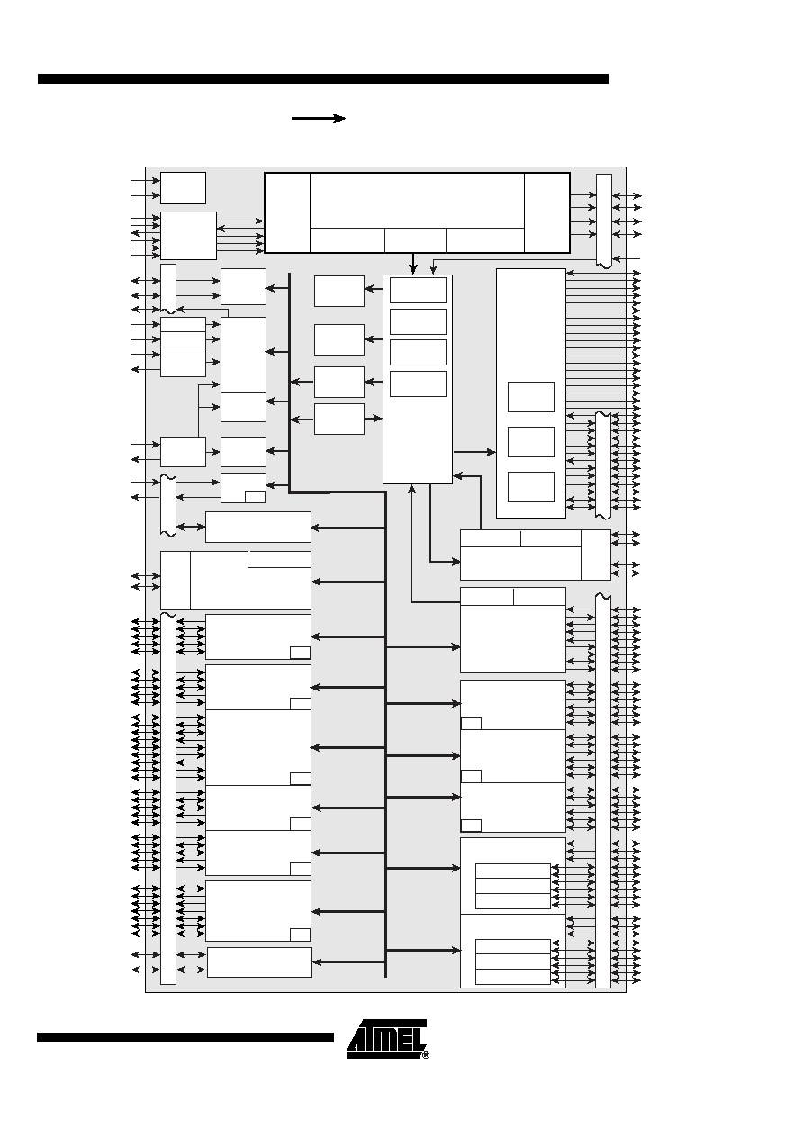
The AT91RM9200 is a complete system-on-chip built around the ARM920T ARM Thumb pro-
cessor. It incorporates a rich set of system and application peripherals and standard interfaces
in order to provide a single-chip solution for a wide range of compute-intensive applications
that require maximum functionality at minimum power consumption at lowest cost.
The AT91RM9200 incorporates a high-speed on-chip SRAM workspace, and a low-latency
External Bus Interface (EBI) for seamless connection to whatever configuration of off-chip
memories and memory-mapped peripherals is required by the application. The EBI incorpo-
rates controllers for synchronous DRAM (SDRAM), Burst Flash and Static memories and
features specific circuitry facilitating the interface for SmartMedia, CompactFlash and NAND
Flash.
The Advanced Interrupt Controller (AIC) enhances the interrupt handling performance of the
ARM920T processor by providing multiple vectored, prioritized interrupt sources and reducing
the time taken to transfer to an interrupt handler.
The Peripheral Data Controller (PDC) provides DMA channels for all the serial peripherals,
enabling them to transfer data to or from on- and off-chip memories without processor inter-
vention. This reduces the processor overhead when dealing with transfers of continuous data
streams.The AT91RM9200 benefits from a new generation of PDC which includes dual point-
ers that simplify significantly buffer chaining.
The set of Parallel I/O (PIO) controllers multiplex the peripheral input/output lines with general-
purpose data I/Os for maximum flexibility in device configuration. An input change interrupt,
open drain capability and programmable pull-up resistor is included on each line.
The Power Management Controller (PMC) keeps system power consumption to a minimum by
selectively enabling/disabling the processor and various peripherals under software control. It
uses an enhanced clock generator to provide a selection of clock signals including a slow
clock (32 kHz) to optimize power consumption and performance at all times.
The AT91RM9200 integrates a wide range of standard interfaces including USB 2.0 Full
Speed Host and Device and Ethernet 10/100 Base-T Media Access Controller (MAC), which
provides connection to a extensive range of external peripheral devices and a widely used net-
working layer. In addition, it provides an extensive set of peripherals that operate in
accordance with several industry standards, such as those used in audio, telecom, Flash
Card, infrared and Smart Card applications.
To complete the offer, the AT91RM9200 benefits from the integration of a wide range of debug
features including JTAG-ICE, a dedicated UART debug channel (DBGU) and an embedded
real time trace. This enables the development and debug of all applications, especially those
with real-time constraints.

4
AT91RM9200
1768B≠ATARM≠08/03
Key Features
This section presents the key features of each block.
ARM920T
Processor
∑
ARM9TDMI
TM
-based on ARM
Æ
Architecture v4T
∑
Two instruction sets
≠
ARM
Æ
High-performance 32-bit Instruction Set
≠
Thumb
Æ
High Code Density 16-bit Instruction Set
∑
5-Stage Pipeline Architecture:
≠
Instruction Fetch (F)
≠
Instruction
Decode (D)
≠
Execute (E)
≠
Data Memory (M)
≠
Register Write (W)
∑
16-Kbyte Data Cache, 16-Kbyte Instruction Cache
≠
Virtually-addressed 64-way Associative Cache
≠
8 words per line
≠
Write-though and write-back operation
≠
Pseudo-random or Round-robin replacement
≠
Low-power CAM RAM implementation
∑
Write Buffer
≠
16-word Data Buffer
≠
4-address Address Buffer
≠
Software Control Drain
∑
Standard ARMv4 Memory Management Unit (MMU)
≠
Access permission for sections
≠
Access permission for large pages and small pages can be specified separately for
each quarter of the pages
≠
16 embedded domains
≠
64 Entry Instruction TLB and 64 Entry Data TLB
∑
8-, 16-, 32-bit Data Bus for Instructions and Data
Debug and Test
∑
Integrated Embedded In-Circuit-Emulator
∑
Debug Unit
≠
Two-pin UART
≠
Debug Communication Channel
≠
Chip ID Register
∑
Embedded Trace Macrocell: ETM9 Rev2a
≠
Medium Level Implementation
≠
Half-rate Clock Mode
≠
Four Pairs of Address Comparators
≠
Two Data Comparators
≠
Eight Memory Map Decoder Inputs
≠
Two Counters
≠
One Sequencer
≠
One 18-byte FIFO

5
AT91RM9200
1768B≠ATARM≠08/03
∑
IEEE1149.1 JTAG Boundary Scan on all Digital Pins
Boot Program
∑
Default Boot Program stored in ROM-based products
∑
Downloads and runs an application from external storage media into internal SRAM
∑
Downloaded code size depends on embedded SRAM size
∑
Automatic detection of valid application
∑
Bootloader supporting a wide range of non-volatile memories
≠
SPI DataFlash
Æ
connected on SPI NPCS0
≠
Two-wire EEPROM
≠
8-bit parallel memories on NCS0 if device integrates EBI
∑
Boot Uploader in case no valid program is detected in external NVM and supporting
several communication media
∑
Serial communication on a DBGU (XModem protocol)
∑
USB Device Port (DFU Protocol)
Embedded
Software Services
∑
Compliant with ATPCS
∑
Compliant with AINSI/ISO Standard C
∑
Compiled in ARM/Thumb Interworking
∑
ROM Entry Service
∑
Tempo, Xmodem and DataFlash services
∑
CRC and Sine tables
Reset Controller
∑
Two reset input lines (NRST and NTRST) providing, respectively:
∑
Initialization of the User Interface registers (defined in the user interface of each
peripheral) and:
≠
Sample the signals needed at bootup
≠
Compel the processor to fetch the next instruction at address zero.
∑
Initialization of the embedded ICE TAP controller.
Memory Controller
∑
Programmable Bus Arbiter handling four Masters
≠
Internal Bus is shared by ARM920T, PDC, USB Host Port and Ethernet MAC
Masters
≠
Each Master can be assigned a priority between 0 and 7
∑
Address Decoder provides selection for
≠
Eight external 256-Mbyte memory areas
≠
Four internal 1-Mbyte memory areas
≠
One 256-Mbyte embedded peripheral area
∑
Boot Mode Select Option
≠
Non-volatile Boot Memory can be internal or external
≠
Selection is made by BMS pin sampled at reset
∑
Abort Status Registers
≠
Source, Type and all parameters of the access leading to an abort are saved
∑
Misalignment Detector
≠
Alignment checking of all data accesses