 | –≠–ª–µ–∫—Ç—Ä–æ–Ω–Ω—ã–π –∫–æ–º–ø–æ–Ω–µ–Ω—Ç: ATA6620 | –°–∫–∞—á–∞—Ç—å:  PDF PDF  ZIP ZIP |

Features
∑
Supply Voltage up to 40V
∑
Operating Voltage V
S
= 5V to 18V
∑
Typically 10 µA Supply Current During Sleep Mode
∑
Typically 40 µA Supply Current in Silent Mode
∑
Linear Low-drop Voltage Regulator:
≠ Normal Mode: V
CC
= 5V ±2%/50 mA
≠ Silent Mode: V
CC
= 5V ±7%/50 mA
≠ Sleep Mode: V
CC
is Switched Off
∑
V
CC
Undervoltage Detection with Reset Output NRES (10 ms Reset Time)
∑
Voltage Regulator is Short-circuit and Over-temperature Protected
∑
LIN Physical Layer According to LIN Specification Revision 2.0
∑
Wake-up Capability via LIN Bus (90 µs Dominant)
∑
TXD Time-out Timer (9 ms)
∑
60V Load-dump Protection at LIN Pin
∑
Bus Pin is Overtemperature and Short-circuit Protected versus GND and Battery
∑
High EMC Level
∑
5V CMOS-Compatible I/O Pins to MCU
∑
ESD HBM 6kV at Pins LIN and VS
∑
Interference and Damage Protection According to ISO/CD7637
∑
Package: SO8
1.
Description
ATA6620 is a fully integrated LIN transceiver, designed according to the LIN specifica-
tion 2.0, with a low-drop voltage regulator (5V/50 mA). The combination of voltage
regulator and bus transceiver makes it possible to develop simple, but powerful, slave
nodes in LIN Bus systems. ATA6620 is designed to handle the low-speed data com-
munication in vehicles (for example, in convenience electronics). Improved slope
control at the LIN driver ensures secure data communication up to 20 kBaud with an
RC oscillator for the protocol handling. The bus output is designed to withstand high
voltage. Sleep mode (voltage regulator switched off) and Silent mode (communication
off; V
CC
voltage on) guarantee minimized current consumption.
LIN Bus
Transceiver
with Integrated
Voltage
Regulator
ATA6620
Preliminary
Rev. 4850A≠AUTO≠02/05
2
4850A≠AUTO≠02/05
ATA6620 [Preliminary]
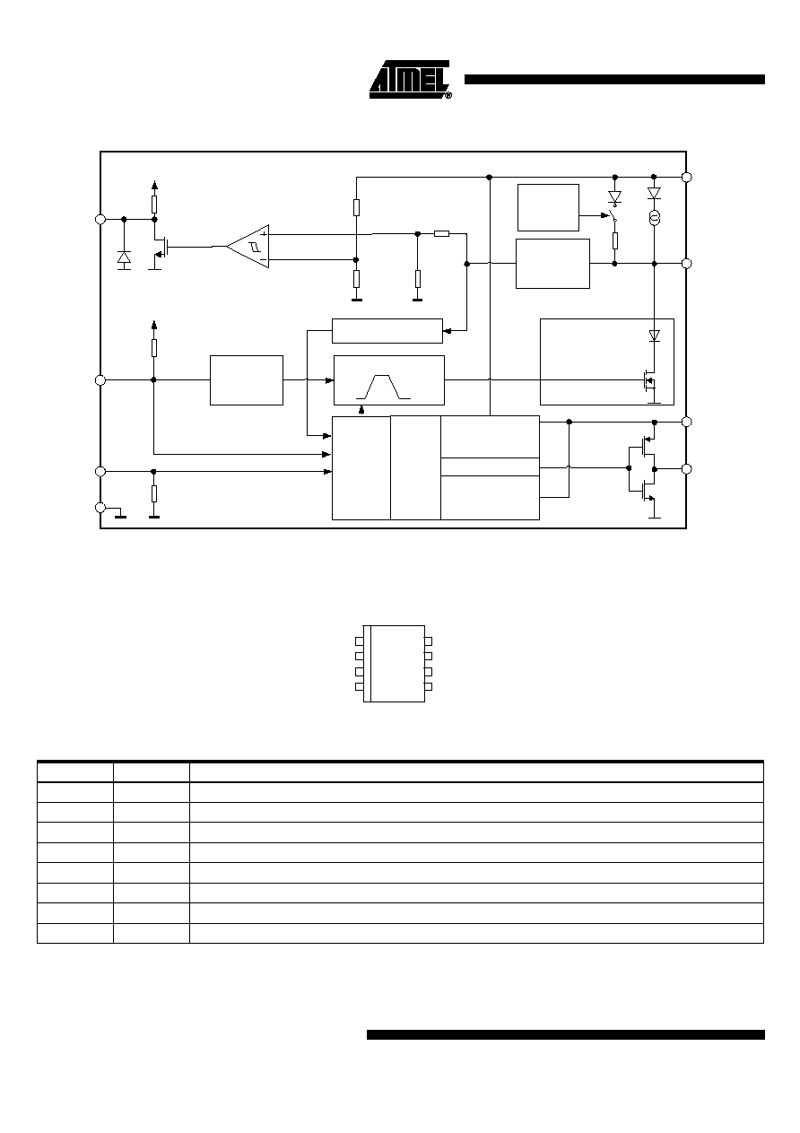
Figure 1-1.
Block Diagram
2.
Pin Configuration
Figure 2-1.
Pinning SO8
VS
NRES
7
4
LIN
1
5
6
RXD
TXD
EN
2
ATA6620
Receiver
Filter
Wake-up Bus Timer
Slew Rate Control
TXD
Time-out
Timer
Control
Unit
Undervoltage Reset
GND
3
VCC
8
Sleep
Mode
VCC
Switched
Off
VCC
Normal and
Pre-normal
Mode
VCC
Normal Mode
Voltage Regulator
5V/50 mA/2%
Silent Mode
Voltage Regulator
5V/50 mA/7%
Short Circuit and
Overtemperature
Protection
1
2
3
4
8
7
6
5
VS
EN
GND
LIN
VCC
NRES
TXD
RXD
Table 2-1.
Pin Description
Pin
Symbol
Function
1
VS
Battery supply
2
EN
Enables Normal mode if the input is high
3
GND
Ground
4
LIN
LIN bus line input/output
5
RXD
Receive data output
6
TXD
Transmit data input
7
NRES
Output undervoltage reset, low at reset
8
VCC
Output voltage regulator 5V/50 mA

3
4850A≠AUTO≠02/05
ATA6620 [Preliminary]
3.
Functional Description
3.1
Supply Pin (VS)
LIN operating voltage is V
S
= 5V to 18V. An undervoltage detection is implemented to disable
transmission if V
S
falls below 5V, in order to avoid false bus messages. After switching on V
S
,
the IC starts with the Pre-normal mode and the voltage regulator is switched on (that is,
5V/50 mA output capability).
The supply current in Sleep mode is typically 10 µA and 40 µA in Silent mode.
3.2
Ground Pin (GND)
The IC is neutral on the LIN pin in case of GND disconnection. It is able to handle a ground shift
up to 3V for supply voltage above 9V at the VS pin.
3.3
Voltage Regulator Output Pin (VCC)
The internal 5V voltage regulator is capable of driving loads with up to 50 mA, supplying the
microcontroller and other ICs on the PCB. It is protected against overload by means of current
limitation and overtemperature shut-down. Furthermore, the output voltage is monitored and will
cause a reset signal at the NRES output pin if it drops below a defined threshold V
thun
.
3.4
Undervoltage Reset Output (NRES)
This push-pull output is supplied from the V
CC
voltage. If the V
CC
voltage falls below the under-
voltage detection threshold of V
thun
, NRES switches to low after tres_f (
Figure 4-6 on page 9
).
Even if V
CC
= 0V the NRES stays low, because it is internally driven from the V
S
voltage. If V
S
voltage ramps down, NRES stays low until V
S
< 1.5V and then becomes highly resistant.
The implemented undervoltage delay keeps NRES low for t
Reset
= 10 ms after V
CC
reaches its
nominal value.
3.5
Bus Pin (LIN)
A low-side driver with internal current limitation and thermal shutdown, as well as an internal
pull-up resistor according to LIN specification 2.0 is implemented. The voltage range is from
≠27V to +60V. This pin exhibits no reverse current from the LIN bus to V
S
, even in the case of a
GND shift or V
Batt
disconnection. The LIN receiver thresholds are compatible with the LIN proto-
col specification.
The fall time (from recessive to dominant) and the rise time (from dominant to recessive) are
slope controlled. The output has a short-circuit limitation. This is a self-adapting current limita-
tion; that is, during current limitation, as the chip temperature increases, the current decreases.
3.6
Input Pin (TXD)
This pin is the microcontroller interface to control the state of the LIN output. TXD must be pulled
to ground in order to drive the LIN bus low. If TXD is high or unconnected (internal pull-up resis-
tor), the LIN output transistor is turned off and the bus is in the recessive state.
4
4850A≠AUTO≠02/05
ATA6620 [Preliminary]
3.7
Dominant Time-out Function (TXD)
The TXD input has an internal pull-up resistor. An internal timer prevents the bus line from being
driven permanently in the dominant state. If TXD is forced to low longer than T
DOM
> 4 ms, the
LIN bus driver is switched to the recessive state. To reset this dominant time-out mode, TXD
must be switched to high (>10 µs) before normal data transmission can be started.
3.8
Output Pin (RXD)
This pin reports the state of the LIN bus to the microcontroller. LIN high (recessive state) is
reported by a high level at RXD; LIN low (dominant state) is reported by a low level at RXD. The
output has an internal pull-up structure with typically 5 k
to V
CC
. The AC characteristics are
measured with an external load capacitor of 20 pF.
The output is short-circuit protected. In unpowered mode (that is, V
S
= 0V), RXD is switched off.
3.9
Enable Input Pin (EN)
This pin controls the operation mode of the interface. After power up of V
S
(battery), the IC
switches to Pre-normal mode, even if EN is low or unconnected (internal pull-down resistor). If
EN is high, the interface is in Normal mode.
A falling edge at EN while TXD is still high forces the device to Silent mode. A falling edge at EN
while TXD is low forces the device to Sleep mode.
4.
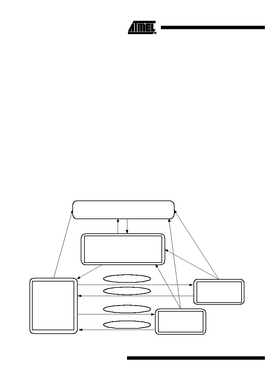
Mode of Operation
Figure 4-1.
Mode of Operation
Pre-normal Mode
VCC: 5V/2%/50 mA with undervoltage reset
Communication: OFF
a
b
Silent Mode
VCC: 5V/7%/50 mA
with undervoltage reset
Communication: OFF
EN = 1
Go to silent command
EN = 0
TXD = 1
Local wake-up event
a: V
S
> 5V
b: V
S
< 4V
c: Bus wake-up event
b
EN = 1
b
c
Normal Mode
VCC: 5V/2%/50 mA
with undervoltage reset
Communication: ON
Unpowered Mode
V
Batt
= 0V
Sleep Mode
VCC: switched off
Communication: OFF
Go to sleep command
Local wake-up event
EN = 0
TXD = 0
EN = 1
b
c
5
4850A≠AUTO≠02/05
ATA6620 [Preliminary]
4.1
Normal Mode
This is the normal transmitting and receiving mode of the LIN Interface, in accordance with LIN
specification 2.0. The V
CC
voltage regulator operates with a 5V output voltage, with a low toler-
ance of ±2% and a maximum output current of 50 mA.
If an undervoltage condition occurs, NRES is switched to low and the ATA6620 changes state to
Pre-normal mode. All features are available.
4.2
Silent Mode
A falling edge at EN while TXD is high switches the IC into Silent mode. The TXD Signal has to
be logic high during the Mode Select window (
Figure 4-2 on page 6
). For EN and TXD either two
independent outputs can be used, or two outputs from the same microcontroller port; in the sec-
ond case, the mode change is only one command.
In Silent mode the transmission path is disabled. Supply current from V
Batt
is typically
I
VSsi
= 40 µA with no load at the V
CC
regulator.
The overall supply current from V
Batt
is the result of 40 µA plus the V
CC
regulator output current
I
VCCs
.
The 5V regulator is in low tolerance mode (4.65V to 5.35V) and can source up to 50 mA. In
Silent mode the internal slave termination between pin LIN and pin VS is disabled to minimize
the power dissipation in case pin LIN is short-circuited to GND. Only a weak pull-up current (typ-
ically 10 µA) between pin LIN and pin VS is present.
The Silent mode voltage is sufficient to run an external microcontroller on the ECU, for example
in Power Down mode. The undervoltage reset is V
CCthS
< 4.4V. If an undervoltage condition
occurs, NRES is switched to low and the ATA6620 changes state to Pre-normal mode.
A falling edge at pin LIN followed by a dominant bus level maintained for a certain time period
(T
bus
) results in a remote wake-up request. The device switches from Silent mode to Pre-normal
mode, then the internal LIN slave termination resistor is switched on. The remote wake-up
request is indicated by a low level at pin RXD to interrupt the microcontroller. (
Figure 4-5 on
page 8
)
With EN high, ATA6620 switches directly from Silent to Normal mode.
Table 4-1.
Mode of Operation
Mode of
Operation
Communication
V
CC
RXD
LIN
Pre-normal OFF
5V
5V
Recessive
Normal
ON
5V
5V
Recessive
Silent
OFF
5V
5V
Recessive
Sleep
OFF
0V
0V
Recessive