 | –≠–ª–µ–∫—Ç—Ä–æ–Ω–Ω—ã–π –∫–æ–º–ø–æ–Ω–µ–Ω—Ç: ATA6660 | –°–∫–∞—á–∞—Ç—å:  PDF PDF  ZIP ZIP |
1
Features
∑
Usable for Automotive 12 V/24 V and Industrial Applications
∑
Maximum High-speed Data Transmissions up to 1 MBaud
∑
Fully Compatible with ISO 11898
∑
Controlled Slew Rate
∑
Standby Mode
∑
TXD Input Compatible to 3.3 V
∑
Short-circuit Protection
∑
Overtemperature Protection
∑
High Voltage Bus Lines Protection, -40 V to +40 V
∑
High Speed Differential Receiver Stage with a Wide Common Mode Range,
-10 V to +10 V, for High Electromagnetic Immunity (EMI)
∑
Fully Controlled Bus Lines, CANH and CANL to Minimize
Electromagnetic Emissions (EME)
∑
High ESD Protection at CANH, CANL HBM 8 kV, MM 300 V
Description
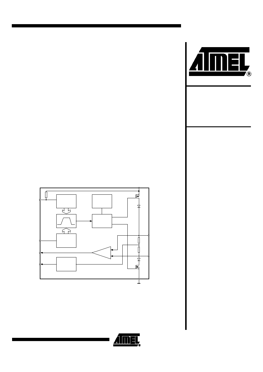
The ATA6660 is a monolithic circuit based on the Atmel's Smart Power BCD60-III
technology. It is especially designed for high speed CAN-Controller (CAN-C) differen-
tial mode data transmission between CAN-Controllers and the physical differential bus
lines.
Figure 1. Block Diagram
4 RXD
5 VREF
7 CANH
6 CANL
8 RS
2 GND
3 VCC
1 TXD
TXD input stage
Constant slope/
standby
Overtemperature
and Short circuit
protection
Driver
Reference
Voltage
0.5*VCC
Receiver
High-speed
CAN
Transceiver
ATA6660
Rev. 4582B≠BCD≠03/03

2
ATA6660
4582B≠BCD≠03/03
Pin Configuration
Figure 2. Pinning SO8
Functional
Description
The ATA6660 is a monolithic circuit based on Atmel's Smart Power BCD60-III technol-
ogy. It is especially designed for high-speed differential mode data transmission in harsh
environments like automotive and industrial applications. Baudrate can be adjusted up
to 1 Mbaud.
The ATA6660 is fully compatible to the ISO11898, the developed standard
for high speed CAN-C (Controller Area Network) communication.
Voltage Protection and
ESD
High voltage protection circuitry on both line pins, CANH (Pin 7) and CANL (Pin 6), allow
bus line voltages in the range of -40 V to +40 V. ESD protection circuitry on line pins
allow HBM = 8 kV, MM = 300 V. The implemented high voltage protection on bus line
output/input pins (7/6) makes the ATA6660 suitable for 12 V automotive applications as
well as 24 V automotive applications.
Slope Control
A fixed slope is adjusted to prevent unsymmetrical transients on bus lines causing EMC
problems. Controlled bus lines, both CANH and CANL signal, will reduce radio fre-
quency interference to a minimum. In well designed bus configurations the filter design
costs can be reduced dramatically.
Overcurrent Protection
In the case of a line shorts, like CANH to GND, CANL to VCC, integrated short current
limitation allows a maximum current of I
CANH_SC
or I
CANL_SC
. If junction temperature rises
above 165
∞
C an internal overtemperature protection circuitry shuts down both output
stages, the receiver will stay activated.
TXD
GND
VCC
RXD
RS
CANH
CANL
VREF
1
2
3
4
8
7
6
5
Pin Description
Pin
Symbol
Function
1
TXD
Transmit data input
2
GND
Ground
3
VCC
Supply voltage
4
RXD
Receive data output
5
VREF
Reference voltage output
6
CANL
Low level CAN voltage input/output
7
CANH
High level CAN voltage input/output
8
RS
Switch standby mode/normal mode

3
ATA6660
4582B≠BCD≠03/03
Standby Mode
T h e A T A 6 6 6 0 c a n b e s w i t c h e d t o s t a n d b y m o d e b y f o r c i n g t h e v o l t a g e
VRS > 0.87
¥
VCC. In standby mode the supply current will reduce dramatically, supply
current during standby mode is typical 600 µA (I
VCC_stby
). Transmitting data function will
not be supported, but the oppertunity will remain to receive data. A high-speed compar-
ator is listening for activities on the bus. A dominant bus signal will force the output RXD
to a low level in typical t
dRXDL
= 400 ns. If the RS pin is not connected, causing through a
broken connection to the controller, the ATA6660 will switch to standby mode
automatically.
High-speed Receiver
In normal mode a fast receiver circuitry combined with a resistor network is able to
detect differential bus line voltages V
rec_th
> 0.9 V as dominant bit, differential bus line
voltages V
rec_th
< 0.5 V as recessive bit.
The wide receiver common mode range, -10 V to +10 V, combined with a symmetrical
differential receiver stage offers high immunity against electromagnetic interference. A
typical hysteresis of 70 mV is implemented. Dominant differential bus voltages forces
RXD output (Pin 4) to low level, recessive differential bus voltages to high level.
TXD Input
The input stage Pin 1 (TXD) is compatible for 3.3 V output levels from new controller
families. Pull-up resistance (25 k
W
) forces the IC to recessive mode, if TXD-Pin is not
connected. TXD low signal drives the transmitter into dominant state.
Transmitter
A integrated complex compensation technique allows stable data transmission up to
1 MBaud. Low level on TXD input forces bus line voltages CANH to 3.5 V, CANL to
1.5 V with a termination resistor of 60
W
. In the case of a line short circuit, like CANH to
GND, CANL to VCC, integrated short current limitation circuitry allows a maximum cur-
rent of 150 mA. If junction temperature rises above typical 163
∞
C an internal
overtemperature protection shuts down both output stages, the receive mode will stay
activated.
Split Termination
Concept
With a modified bus termination (see Figure 5) a reduction of emission and a higher
immunity of the bus system can be achieved. The one 120
W
resistor at the bus line end
nodes is split into two resistors of equal value, i.e., two resistors of 60
W.
The resistors
for the stub nodes is recommended with two resistors of 1,3 k
W. (
for example 8 stub
nodes and 2 bus end nodes) Notice: The bus load of all the termination resistors has to
stay within the range of 50
W
to 65
W.
The common mode signal at the centre tap of the termination is connected to ground via
a capacitor of e.g., C
split
= 10 nF to 100 nF. A seperate ground lead to the ground pin of
the module connector is recommended.
4
ATA6660
4582B≠BCD≠03/03
Absolute Maximum Ratings
Parameters
Symbol
Conditions
Min.
Max.
Unit
Supply voltage
V
CC
-0.3
+6
V
DC voltage at Pins 1, 4, 5 and 8
V
TXD
, V
REF
, V
RS
,
V
RXD
-0.3
V
CC
+0.3
V
DC voltage at Pins 6 and 7
V
CANH
, V
CANL
0 V < V
CC
< 5.25 V;
no time limit
-40.0
+40.0
V
Transient voltage at Pins 6 and 7
-150
+100
V
Storage temperature
T
Stg
-55
+150
∞
C
Operating ambient temperature
T
amb
-40
+125
∞
C
ESD classification
All pins
HBM ESD S.5.1
MM JEDEC A115A
±3000
±200
V
V
ESD classification
Pin 6, 7 versus
Pin 2
HBM 1.5 k
W
, 100 pF
MM 0
W
, 200 pF
±8000
±300
V
V
Thermal Resistance
Parameters
Symbol
Value
Unit
Thermal resistance from junction to ambient
R
thJA
160
K/W
Truth Table
VCC
TXD
RS
CANH
CANL
Bus State
RXD
4.75 V to 5.25 V
0
< 0.3
¥
V
CC
3.5 V
1.5 V
Dominant
0
4.75 V to 5.25 V
1 (or floating)
< 0.3
¥
V
CC
0.5
¥
V
CC
0.5
¥
V
CC
Recessive
1
4.75 V to 5.25 V
X
> 0.87
¥
V
CC
0.5
¥
V
CC
0.5
¥
V
CC
Recessive
1
RS (Pin 8) Functionality
Slope Control
Mode
Voltage and Current Levels
V
RS
> 0.87
¥
V
CC
Standby
I
RS
<
| 10 µA
|
V
RS
< 0.3
¥
V
CC
Constant slope control
I
RS
£
500 µA
5
ATA6660
4582B≠BCD≠03/03
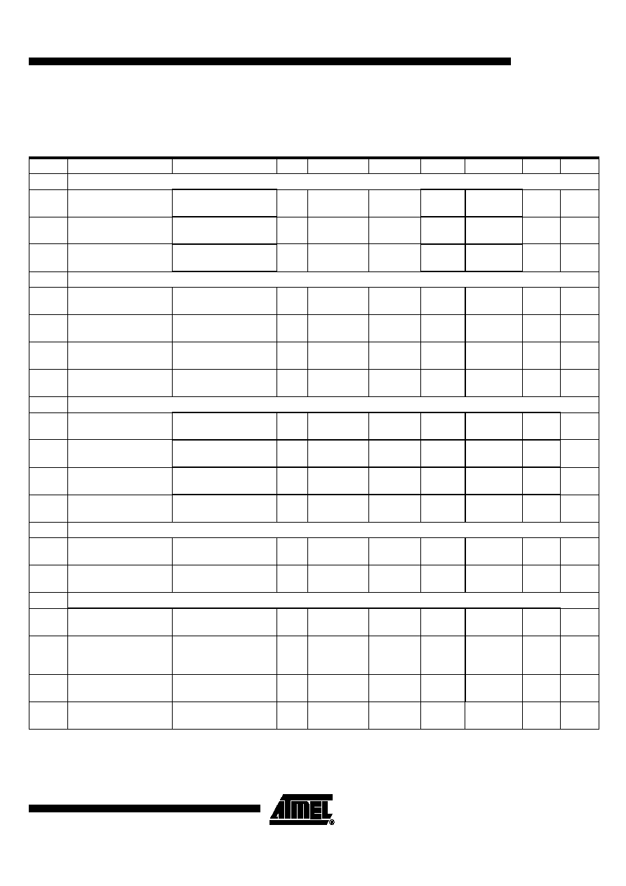
Electrical Characteristics
V
CC
= 4.75 V to 5.25 V; T
amb
= -40
∞
C to +125
∞
C; R
Bus
= 60
; unless otherwise specified
All voltages referenced to ground (Pin 2); positive input current.
No.
Parameters
Test Conditions
Pin
Symbol
Min.
Typ.
Max.
Unit
Type*
1
Supply Current
1.1
Supply current
dominant
V
TXD
= 0 V
V
RS
= 0 V
3
I
vcc_dom
45
60
mA
A
1.2
Supply current
recessive
V
TXD
= 5 V
V
RS
= 0 V
3
I
vcc_rec
10
15
mA
A
1.3
Supply current stand-
by
V
RS
= 5 V
3
I
vcc_stby
600
980
µA
A
2
Transmitter Data Input TXD
2.1
HIGH level input
voltage
V
TXD
= 5 V
V
RS
= 0 V
1
V
TXDH
2
V
CC
+0.3
V
A
2.2
LOW level input
voltage
V
TXD
= 0 V
V
RS
= 0 V
1
V
TXDL
-0.3
+1
V
A
2.3
HIGH level input
current
V
TXD
= V
CC
1
I
IH
-1
0
µA
A
2.4
LOW level input
voltage
V
TXD
= 0 V
1
I
IL
-500
-50
µA
A
3
Receiver Data Output RXD
3.1
High level output
voltage
I
RXD
= -100 µA
4
V
RXDH
0.8
¥
V
CC
V
CC
V
A
3.2
Low level output
voltage
I
RXD
= 1 mA
4
V
RXDL
0
0.2
¥
V
CC
V
A
3.3
Short current at RXD
V
TXD
= 5 V
V
RXD
= 0 V
4
I
RXDs1
-3
-1
mA
A
3.4
Short current at RXD
V
TXD
= 0 V
V
RXD
= 5 V
4
I
RXDs2
2
6
mA
A
4
Reference Output Voltage VREF
4.1
Reference output
voltage normal mode
VRS = 0 V;
-50 µA < I5 < 50 µA
5
V
ref_no
0.45 V
CC
-
0.55 V
CC
V
A
4.2
Reference output
voltage standby mode
VRS = 5 V;
-5µA < I5 < 5 µA
5
V
ref_stby
0.4
¥
V
CC
-
0.6 V
CC
V
A
5
DC Bus Transmitter CANH; CANL
5.1
Recessive bus
voltage
V
TXD
= V
CC
; no load
6, 7
V
CANH
;
V
CANL
2.0
2.5
3.0
V
A
5.2
I
O(CANH)(reces)
I
O(CANL)(reces)
-40 V < V
CANH;
V
CANL
< 40 V;
0 V < V
CC
< 5.25 V
6, 7
I
O_reces
-5
+5
mA
A
5.3
CANH output voltage
dominant
V
TXD
= 0 V
6, 7
V
CANH
2.8
3.5
4.5
V
A
5.4
CANL output voltage
dominant
V
TXD
= 0 V
6, 7
V
CANL
0.5
1.5
2.0
V
A
*) Type means: A = 100% tested, B = 100% correlation tested, C = Characterized on samples, D = Design parameter