ATF22LV10CZ
High
Performance
E
2
PLD
ATF22LV10CZ
Pin Configurations
Pin Name
Function
CLK
Clock
IN
Logic Inputs
I/O
Bidirectional Buffers
V
CC
(3 to 5.5V) Supply
Features
∑
3.0V to 5.5V Operating Range
∑
Advanced Low Voltage, Zero Power,
Electrically Erasable Programmable Logic Device
∑
Edge-Sensing "Zero" Power
∑
Low Voltage Equivalent of ATF22V10CZ
∑
"Zero" Standby Power (25
µ
A Maximum)
∑
Ideal for Battery Powered Systems
∑
25 ns Maximum Propagation Delay
∑
CMOS and TTL Compatible Inputs and Outputs
∑
Latch Feature Hold Inputs to Previous Logic States
∑
Advanced E
2
Technology
Reprogrammable
100% Tested
∑
High Reliability CMOS Process
20 Year Data Retention
100 Erase/Write Cycles
2,000V ESD Protection
200 mA Latchup Immunity
∑
Commercial and Industrial Temperature Ranges
∑
Dual-in-Line and Surface Mount Standard Pinouts
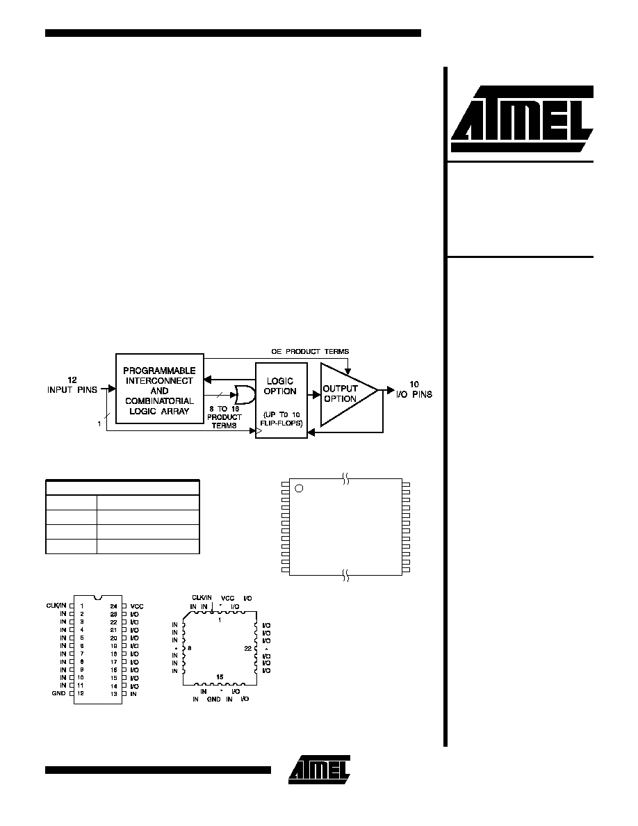
Block Diagram
DIP/SOIC
PLCC
Note: For PLCC, pins 1, 8, 15, and 22 can be left unconnected. For supe-
rior performance, connect V
CC
to pin 1 and GND to pins 8, 15, and 22.
Top view
Rev. 0779E/LV10CZ-E≠05/98
1
2
3
4
5
6
7
8
9
10
11
12
24
23
22
21
20
19
18
17
16
15
14
13
CLK/IN
IN
IN
IN
IN
IN
IN
IN
IN
IN
IN
GND
VCC
I/O
I/O
I/O
I/O
I/O
I/O
I/O
I/O
I/O
I/O
IN
TSSOP Top View

DC and AC Operating Conditions
Commercial
Industrial
Operating Temperature (Case)
0∞C - 70∞C
-40∞C - 85∞C
V
CC
Power Supply
3.0V - 5.5V
3.0V - 5.5V
Description
The ATF22LV10CZ is a high performance CMOS (Electri-
cally Erasable) Programmable Logic Device (PLD) which
utilizes Atmel's proven electrically erasable Flash mem-
ory technology and provides 25 ns speed with stand-by
current of 25
µ
A maximum. All speed ranges are specified
over the 3.0V to 5.5V range for industrial and commercial
temperature ranges.
The ATF22LV10CZ provides a low voltage and edge-
sensing "zero" power CMOS PLD solution with "zero"
standby power (5
µ
A typical). The ATF22LV10CZ powers
down automatically to the zero power mode through At-
mel's patented Input Transition Detection (ITD) circuitry
when the device is idle. The ATF22LV10CZ is capable of
operating at supply voltages down to 3.0V. Pin "keeper"
circuits on input and output pins hold pins to their previous
logic levels when idle, which eliminate static power con-
sumed by pull-up resistors.
The ATF22LV10CZ macrocell incorporates a variable
product term architecture. Each output is allocated from 8
to 16 product terms which allows highly complex logic
functions to be realized. Two additional product terms are
included to provide synchronous reset and asynchronous
reset. These additional product terms are common to all
10 registers and are automatically cleared upon power up.
Register Preload simplifies testing. A Security Fuse pre-
vents unauthorized copying of programmed fuse patterns.
Temperature Under Bias................... -40∞C to +85∞C
Storage Temperature...................... -65∞C to +150∞C
Voltage on Any Pin with
Respect to Ground......................... -2.0V to +7.0V
(1)
Voltage on Input Pins
with Respect to Ground
During Programming.................... -2.0V to +14.0V
(1)
Programming Voltage with
Respect to Ground....................... -2.0V to +14.0V
(1)
*NOTICE: Stresses beyond those listed under "Absolute Maxi-
mum Ratings" may cause permanent damage to the device.
This is a stress rating only and functional operation of the
device at these or any other conditions beyond those indi-
cated in the operational sections of this specification is not
implied. Exposure to absolute maximum rating conditions
for extended periods may affect device reliability.
Absolute Maximum Ratings*
Note:
1. Minimum voltage is -0.6V dc, which may undershoot
to -2.0V for pulses of less than 20 ns. Maximum out-
put pin voltage is Vcc + 0.75V dc, which may over-
shoot to 7.0V for pulses of less than 20 ns.
2
ATF22LV10CZ

Functional Logic Diagram Description
T h e F u n c t i o n a l L o g i c D i a g r a m d e s c r i b e s t h e
ATF22LV10CZ architecture.
The ATF22LV10CZ has 12 inputs and 10 I/O macrocells.
Each macrocell can be configured into one of four output
configurations: active-high/low or registered/combinato-
rial. The universal architecture of the ATF22LV10CZ can
be programmed to emulate most 24-pin PAL devices.
Unused product terms are automatically disabled by the
compiler to decrease power consumption. A Security
Fuse, when programmed, protects the contents of the
ATF22LV10CZ. Eight bytes (64 fuses) of User Signature
are accessible to the user for purposes such as storing
project name, part number, revision or date. The User
Signature is accessible regardless of the state of the Se-
curity Fuse.
DC Characteristics
Symbol Parameter
Condition
Min
Typ
Max
Units
I
IL
Input or I/O Low
Leakage Current
0
V
IN
V
IL
(MAX)
-10
µ
A
I
IH
Input or I/O High
Leakage Current
V
CC
- 0.7V
V
IN
V
CC
10
µ
A
I
CC
Clocked Power
Supply Current
V
CC
= MAX,
Outputs Open, f = 15 MHz
Com.
55
85
mA
Ind.
60
90
mA
I
SB
Power Supply Current,
Standby
V
CC
= MAX,
V
IN
= MAX, Outputs Open
Com.
5
25
µ
A
Ind.
5
50
µ
A
I
OS
(1)
Output Short Circuit
Current
V
OUT
= 0.5V
-130
mA
V
IL
Input Low Voltage
-0.5
0.8
V
V
IH
Input High Voltage
2.0
V
CC
+ 0.75
V
V
OL
Output Low Voltage
V
IN
= V
IH
or V
IL
V
CC
= MIN,
I
OL
= 8 mA
Com.
Ind.
0.5
V
V
OH
Output High Voltage
V
IN
= V
IH
or V
IL
,
V
CC
= MIN,
I
OH
= -4.0 mA
2.4
V
Note: 1. Not more than one output at a time should be shorted. Duration of short circuit test should not exceed 30 sec.
ATF22LV10CZ
3

AC Waveforms
AC Characteristics
(1)
Symbol
Parameter
-25
Min
Max
Units
t
PD
Input to Feedback to Non-Registered Output
3
25
ns
t
CF
Clock to Feedback
13
ns
t
CO
Clock to Output
2
15
ns
t
S
Input or Feedback Setup Time
15
ns
t
H
Input Hold Time
0
ns
t
P
Clock Period
25
ns
t
W
Clock Width
12.5
ns
F
MAX
External Feedback 1/(t
S
+ t
CO
)
Internal Feedback 1/(t
S
+ t
CF
)
No Feedback 1/(t
P
)
33.3
35.7
40.0
MHz
MHz
MHz
t
EA
Input to Output Enable
3
25
ns
t
ER
Input to Output Disable
3
25
ns
t
AP
Input or I/O to Asynchronous Reset of Register
3
25
ns
t
SP
Setup Time, Synchronous Preset
15
ns
t
AW
Asynchronous Reset Width
25
ns
t
AR
Asynchronous Reset Recovery Time
25
ns
t
SPR
Synchronous Preset to Clock Recovery Time
15
ns
Note:
1. See ordering information for valid part numbers.
INPUTS, I/O
REG. FEEDBACK
SYNCH. PRESET
CP
ASYNCH. RESET
REGISTERED
OUTPUTS
COMBINATORIAL
OUTPUTS
VALID
VALID
VALID
VALID
VALID
VALID
OUTPUT
DISABLED
OUTPUT
DISABLED
tS
tH
tW
tW
tP
tAR
tAW
tAP
tCO
tPD
tER
tEA
tEA
tER
4
ATF22LV10CZ
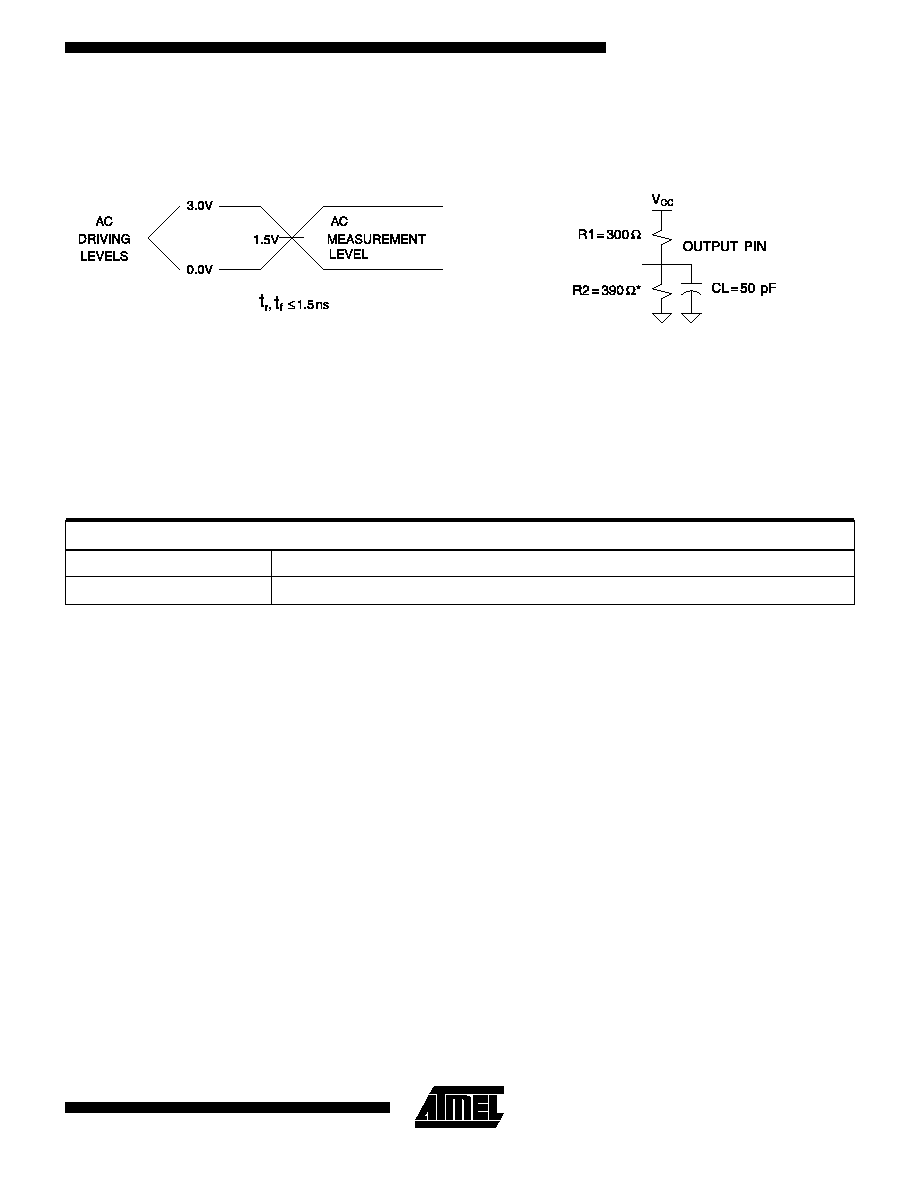
Input Test Waveforms and
Measurement Levels
Note:
Similar competitors' devices are specified
with slightly different loads. These load differ-
ences may affect output signals' delay and slew
rate. Atmel devices are tested with sufficient
margins to meet compatible device specification
conditions.
Output Test Loads
Pin Capacitance
(f = 1 MHz, T = 25∞C)
(1)
Typ
Max
Units
Conditions
C
IN
5
8
pF
V
IN
= 0V
C
OUT
6
8
pF
V
OUT
= 0V
Note:
1. Typical values for nominal supply voltage. This parameter is only sampled and is not 100% tested.
ATF22LV10CZ
5