 | –≠–ª–µ–∫—Ç—Ä–æ–Ω–Ω—ã–π –∫–æ–º–ø–æ–Ω–µ–Ω—Ç: ATLV | –°–∫–∞—á–∞—Ç—å:  PDF PDF  ZIP ZIP |
ATLV
1
ATLV Series
Ultra Low
Voltage
Gate Arrays
Features
∑
Specifically Designed for Battery Powered Applications
1.0 - 3.0 Volts and will Operate from 0.7 to 5.5 Volts
∑
Static Current Drain of <75 nA at 1.0 Volts
∑
200 MHz Maximum Toggle Frequency for Flip Flop at 1.5 Volts
∑
1.0
µ
Drawn Gate Length CMOS Gate Arrays
∑
All Package Styles Offered Including TQFP and TAB
∑
Improved Product Testability Using Serial Scan, Boundary Scan,
and JTAG
∑
Second Source Existing ASIC Design in Atmel's ATLV via Design
Translation. Improved Performance and Lower Cost
ATLV Array Organization
Device
Raw
Routable
Max Pin
Max I/O
(1)
Gate
(2)
Number
Gates
Gates
Count
Pins
Speed
ATLV2
2,000
1,400
44
36
1.3 ns
ATLV3
3,000
1,600
68
60
1.3 ns
ATLV5
5,000
2,800
84
76
1.3 ns
ATLV7
7,000
4,400
100
92
1.3 ns
ATLV10
10,000
6,600
120
112
1.3 ns
ATLV15
15,000
8,000
144
136
1.3 ns
ATLV20
22,000
12,000
160
152
1.3 ns
ATLV35
35,000
18,000
208
192
1.3 ns
Notes: 1. Absolute maximum I/O pins is maximum pin count minus 8. Additional power
and ground pins are assumed to be required to support simultaneous
switching outputs as pin count increases.
2. Nominal 2 input nand gate with a fan out of 2 at 1.5 volts, room temperature.
ATLV2
ATLV3
ATLV5
ATLV7
ATLV10
ATLV15
ATLV20
ATLV35
Description
The ATLV Series CMOS gate arrays employ 1.0
µ
-drawn, double-level metal,
Si-gate, CMOS technology processed in Atmel's U.S.-based, advanced
manufacturing facility. The arrays utilize an enhanced channelless architecture
which results in greater than 50 percent usable gates.
Atmel's flexible design system uses industry design standards and is compatible
with popular CAD/CAE software and hardware packages. The customer can
start designing with the ATLV series today using existing CAD/CAE tools.
0261B
ATLV
2
ATLV Design
Design Systems Supported
Atmel supports the major CAE/CAD software systems
with complete macro cell libraries (symbols, timing and
function), as well as utilities for checking the netlist and
accurate pre-route delay simulations. Atmel uses Cadence's
Verilog-XL as our golden simulator. Design systems
which are supported include Cadence, Viewlogic, Mentor,
and Synopsys.
Design Flow
While Atmel provides four options for implementing a gate
array design, they all have the same basic flow. Data base
acceptance is the first milestone. This is when Atmel
receives and accepts the complete design data base.
Preliminary design review is where the performance of the
design is set based on the Cadence simulation. Final design
review is the last review of the design before making masks.
The back annotation data is incorporated into the simulations.
After final design review masks are released and prototypes
in ceramic packages are delivered.
Design Options
Schematic Capture
Schematic capture and simulation are performed by the
customer using an Atmel supplied macro cell library. The
customer can also receive complete back annotation delay
data for post-route simulation.
VHDL/Verilog-HDL
Atmel can accept Register Transfer level (RTL) designs for
VHDL (MIL-STD-454, IEEE STD 1076) or Verilog-HDL
format. Atmel fully supports Synopsys for VHDL simula-
tion as well as synthesis. Design via VHDL or Verilog-
HDL is the preferred method of performing a gate array
design.
ASIC Design Translation
Atmel has successfully translated dozens of existing de-
signs from most major ASIC vendors (LSI Logic, Oki,
NEC, Fujitsu and others) into our gate arrays. These
designs have been optimized for speed, gate count, modi-
fied to add logic or memory, or replicated for a pin-for-pin
compatible, drop-in replacement.
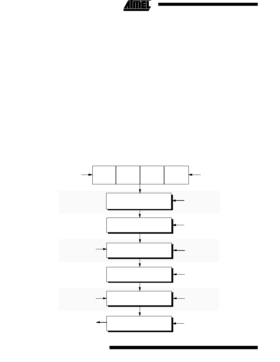
ATLV Gate Array Design Flow
Atmel Cell
Library
Gate Array
Design
Translation
Design
Synthesis
-VHDL
-Verilog-HDL
FPGA/EPLD
Conversions
Customer
Atmel
Final Design Review
Prototype Delivery
Atmel
Atmel
Simulation
and Verification
Atmel
Customer
Customer
Atmel
Atmel
Preliminary Design Review
Physical Design, Simulation
and Verification
Atmel
Data Base Acceptance
Customer
ATLV
3
FPGA and EPLD Conversions
Atmel has successfully translated existing FPGA/EPLD
designs from most major vendors (Xilinx, Actel, Altera,
AMD & Atmel) into our gate arrays. The design can be
optimized for speed or power consumption, modified to
add logic or memory or replicated for a pin-for-pin compat-
ible, drop-in replacement. Atmel frequently combines
several devices onto a single gate array.
at the transistor level and verified through measurements
made on fabricated test arrays. The symbols for the ATLV
cell library are compatible with Atmel's ATL (1.0
µ
3.3
and 5.0 V) and ATL80 (0.8
µ
3.3 and 5.0 V) cell libraries.
Existing designs can be easily migrated to the ATLV
series. Characterization has been performed over
commercial temperature and 1.0 to 3.0 volts, to ensure
that the simulation accurately predicts the performance
of the finished product. Atmel is continually expanding
the ATLV series cell library with both soft and hard
macros. Check with your sales representative for the most
recent additions.
ATLV Series Cell Library
Atmel's ATLV series gate arrays use cells from an
accurately modeled and highly flexible library. The cell
library contains over 120 hard-wired data path elements
and has been characterized via extensive SPICE modeling
AND, NAND, OR, NOR Gates
2 input AND
2 input NOR
3 input AND
Dual 2 input NOR
4 input AND
3 input NOR
5 input AND
4 input NOR
2 input NAND
5 input NOR
Dual 2-input NAND
8 input NOR
3 input NAND
2 input OR
4 input NAND
3 input OR
5 input NAND
4 input OR
6 input NAND
8 input NAND
Cell Guide
Buffers and Inverters
1x Buffer
1x Inverter
2x Buffer
Dual 1x Inverter
2x Buffer with Enable
Quad 1x Inverter
2x Buffer with Enable Low
Quad Tri-state Inverter
3x Buffer
2x Inverter
4x Buffer
Dual 2x Inverter
8x Buffer
2x Tri-state Inverter
12x Buffer
3x Inverter
16x Buffer
4x Inverter
Delay Buffer 2.0 ns
8x Inverter
Delay Buffer 3.5 ns
10x Inverter
Delay Buffer 8.0 ns
Multiplexers
2:1 MUX
4:1 MUX
Inverting 2:1 MUX w/o Buffered Inputs
4:1 MUX w/o Buffered Inputs
Inverting 2:1 MUX w/o Buffered Inputs
4:1 MUX w/o Buffered Inputs
2:1 MUX with Enable Low
8:1 MUX
Quad 2:1 MUX with Enable
8:1 MUX with Enable Low
Quad 2:1 MUX
Inverting 3:1 MUX w/o Buffered Inputs
Inverting 3:1 MUX w/o Buffered Inputs
ATLV
4
Cell Guide
Exclusive OR/NOR Gates
1 bit Adder
2 input Exclusive OR
1 bit Adder with Buffered Outputs
2 input Exclusive NOR
7 input Carry Lookahead
AND/OR, OR/AND Gates
3 input AND OR INVERT
3 input OR AND INVERT
4 input AND OR INVERT
4 input OR AND INVERT
6 input AND OR INVERT
8 input OR AND INVERT
Decoders
2:4 Decoder
3:8 Decoder with Low Enable
2:4 Decoder with Low Enable
Flip-flops/Latches
D Flip-flop
LATCH
D Flip-flop with Clear/Preset
LATCH with Complementary Outputs
D Flip-flop with Clear
LATCH with Inverted Gate Signal
D Flip-flop with Reset
QUAD LATBG with Common Gate Signal
D Flip-flop with Set
QUAD Inverting LATCH
D Flip-flop with Set/Reset
LATCH with Reset
JK Flip-flop
LATCH with Set
JK Flip-flop with Clear/Preset
LATCH with Set and Reset
JK Flip-flop with Clear
Scan Cells
Set-scan Register
Set-scan Register with Set
Set-scan Register with Clear and Preset
Set-scan Register with Set and Reset
Set-scan Register with Reset
I/O Options
Input, Output, Bidirectional, Tristate Output, Internal Clock Driver and Oscillator
Output Drive Value Programmable from 0.5 mA to 6 mA in 0.5 mA increments with Slew Rate Control
CMOS Operation
Testable NAND Gate on Input (Bidirectional, Input)
Inverting and Non-inverting Input Buffers (Bidirectional, Input)
Pullup Resistor - 10K
to 310K
Pulldown Resistor - 3.5K
to 108.5K
ATLV
5
CMOS Input Interface Characteristics
V
IH
CMOS Input High Voltage
0.8 x V
DD
V
V
T
CMOS Switching Threshold
V
DD
=1.5 V, 25
∞
C
0.75
V
V
OL
Output Low Voltage
I
OL
=as rated
0.2 x V
DD
V
Output buffer has
V
DD
=1.5 V
12 stages of drive capability
with 0.5 mA I
OL
per stage.
V
OH
Output High Voltage
I
OH
=as rated
0.8 x V
DD
V
Output buffer has
V
DD
=1.5 V
12 stages of drive capability
with -0.5 mA I
OH
per stage.
I
DD
Static Current
1.0 V
< 75
nA
Input Leakage Low
3.0 V
< 1.0
µ
A
(no pull-up)
I
OS
Output Short Circuit Current
V
DD
=1.8 V, V
OUT
=V
DD
5
25
60
mA
(3 x Buffer)
(2)
V
DD
=1.8 V, V
OUT
=V
SS
-60
-25
-5
mA
V
IL
CMOS Input Low Voltage
0.2 x V
DD
V
I
IH
Input Leakage High
V
IN
=V
DD
, V
DD
=1.8 V
1 x 10
-5
10
µ
A
I
IL
Input Leakage Low
V
IN
=V
SS
, V
DD
=1.8 V
-10
-1 x 10
-5
µ
A
(no pull-up)
I
OZ
Output Leakage (no pull-up)
V
IN
=V
DD
or V
SS
, V
DD
=3.6 V
-10
1 x 10
-5
10
µ
A
Interface
Logic High
Logic Low
Switchpoint
CMOS
0.90 V
DD
0.1 V
DD
V
DD
/2 Typical
Absolute Maximum Ratings*
*NOTICE: Stresses beyond those listed under "Absolute Maximum
Ratings" may cause permanent damage to the device. This is a stress
rating only and functional operation of the device at these or any other
conditions beyond those indicated in the operational sections of this
specification is not implied. Exposure to absolute maximum rating
conditions for extended periods may affect device reliability.
Notes:
1. Minimum voltage is -0.6 V dc which may undershoot to -2.0 V
for pulses of less than 20 ns. Maximum output pin voltage is
V
DD
+ 0.75V dc which may overshoot to +7.0 V for pulses of less
than 20 ns.
Operating Temperature .......................-40
∞
C to +85
∞
C
Storage Temperature ........................ -65
∞
C to +150
∞
C
Voltage on Any Pin
with Respect to Ground ................... .-2.0 V to +5.5 V
1
Maximum Operating Voltage ............................... 5.5 V
Applicable over recommended operating range from T
a
= -40
∞
C to +85
∞
C, V
DD
= 1.0 V to 3.0 V (unless otherwise noted)
1.5 Volt DC Characteristics
Symbol
Parameter
Test Condition
Min
Typ
Max
Units
Note:
2. This is the specification for the 3 x Output Buffer. Output short circuit current for other outputs will scale accordingly. Not more
than one output shorted at a time, for a maximum of one second, is allowed.