 | –≠–ª–µ–∫—Ç—Ä–æ–Ω–Ω—ã–π –∫–æ–º–ø–æ–Ω–µ–Ω—Ç: MH1 | –°–∫–∞—á–∞—Ç—å:  PDF PDF  ZIP ZIP |
Rev. 4138E≠AERO≠06/02
1
Features
∑
High Speed - 170 ps Gate Delay - 2 Input NAND, FO = 2 (Nominal)
∑
Up to 1.6 Million Used Gates and 596 Pads, with 3.3V, 3V, and 2.5V Libraries
∑
System Level Integration Technology Cores on Request: SRAM and TRAM (Gate Level
or Embedded)
∑
I/O Interfaces:
≠ 5V Tolerant/Compliant (S) or 3V (R) Matrix Options
≠ CMOS, LVTTL, LVDS, PCI, USB
≠ Output Currents Programmable from 2 to 24 mA, by Step of 2 mA
∑
250 MHz PLL (On Request), 220 MHz LVDS and 800 MHz Max Toggle Frequency at 3.3V
∑
Deep Submicron CAD Flow
∑
QML Q with SMD 5962-01B01
Description
The MH1 Series Gate Array and Embedded Array families from Atmel are fabricated
in a 0.35 micron CMOS process, with up to four levels of metal. This family features
arrays with up to 1.6 million routable gates and 596 pads. The high density and high
pin count capabilities of the MH1 family, coupled with the ability to embed memories
on the same silicon, make the MH1 series of arrays an ideal choice for System Level
Integration.
The MH1 series is supported by an advanced software environment based on industry
standards linking proprietary and commercial tools. Verilog
Æ
, DFT
Æ
, Synopsys
Æ
and
Vital are the reference front end tools. The Cadence
Æ
`Logic Design Planner' floor
planning associated with timing driven layout provides an efficient back end cycle.
The MH1 series comes as a dual use of the MH1RT series, without the latch up and
total dose immunity features.
The MH1 series comes as the Atmel seventh generation of ASIC series designed for
military and avionics types of applications in a 15-year time frame.
It is also made available to any of the currently available quality grades: commercial,
industrial, automotive and military.
1.6M Used Gates
0.35 µm CMOS
Sea of Gates/
Embedded
MH1
2
MH1
4138E≠AERO≠06/02
Note:
1. Nominal 2 Input NAND Gate FO = 2 at 3 volts.
Design
Design Systems
Supported
Atmel supports several major software systems for design with complete macro cell
libraries, as well as utilities for checking the netlist and accurate pre-route delay
simulations.
The following design systems are supported:
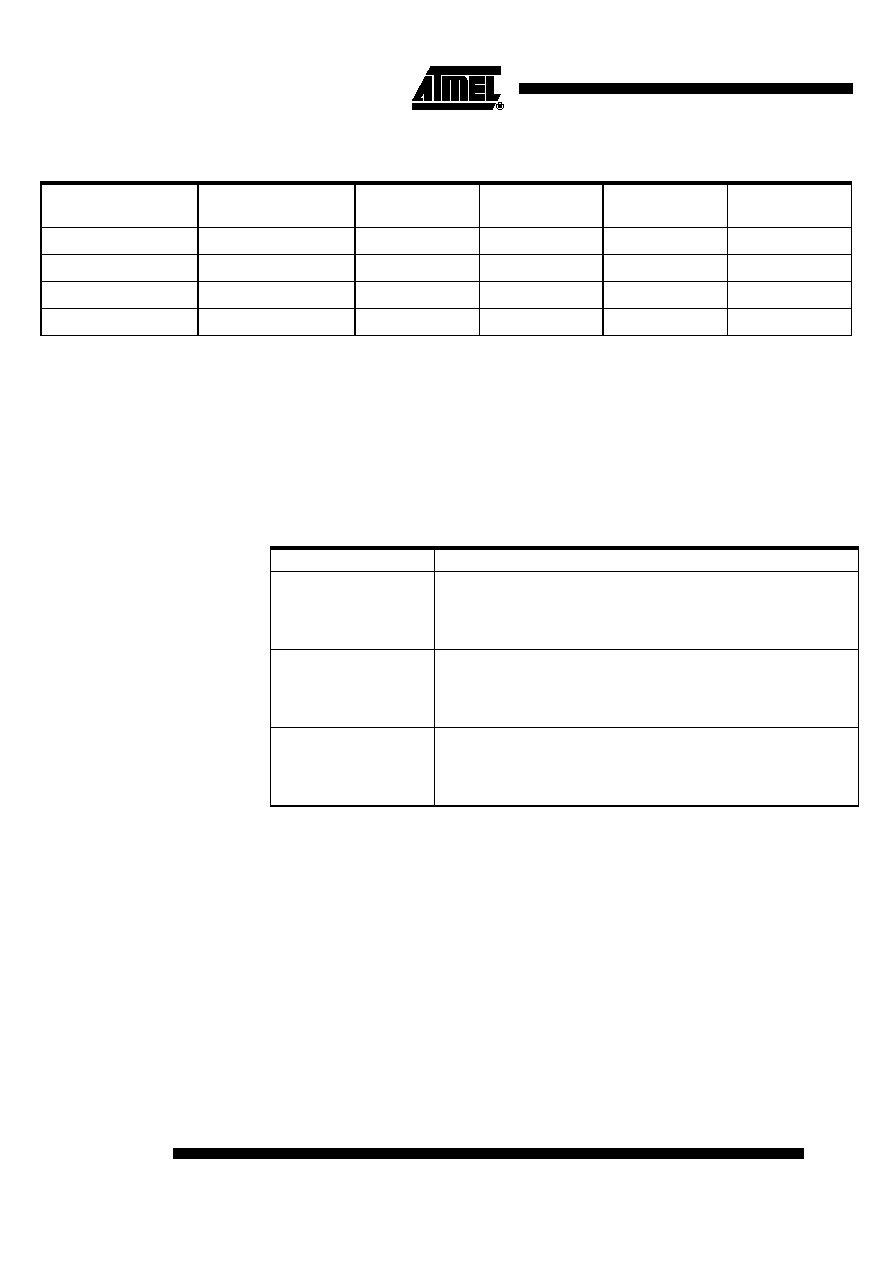
Table 1. MH1 Array Organization
Device
Number
Routable
Gates
Number of Pads
Max
I/O Count
Gate
Speed
(1)
Max Sites
Count
MH1099
519,000
332
324
170 ps
921000
MH1156
764,000
412
404
170 ps
1 452 000
MH1242
1,198,000
512
504
170 ps
2 275 000
MH1332
1,634,000
596
588
170 ps
3 105 000
Table 2. Design Systems Supported
System
Available/Planned Tools
Cadence
Æ
PerlTM - Static Path
Verilog-XLTM - Verilog Simulator
Logic Design Planner
TM
- Floorplanner
BuildGates
Æ
- Synthesis (Ambit)
Mentor/Model TechTM
Modelsim Verilog and VHDL (VITAL) Simulator
Leonardo SpectrumTM - Synthesis
Velocity - Static Path
DFT - Scan Insertion and ATPG, BIST
Synopsys
Æ
Design Compiler
Æ
- Synthesis
Test CompilerTM - Scan Insertion and ATPG
Test-Gen
Æ
- Scan Insertion and ATPG
PrimetimeTM - Static Path

3
MH1
4138E≠AERO≠06/02
Design Flow and
Tools
Design flow for Gate Arrays/Embedded Arrays is structured to allow the designer to con-
solidate the greatest number of system components possible onto the same silicon chip,
using available third party design tools. Atmel's cell library reflects silicon performance
over extremes of temperature, voltage, and process, and includes the effects of metal
loading, inter-level capacitance, and edge rise and fall times. The Design Flow includes
clock tree synthesis to customer specified skew and latency goals. RC extraction is per-
formed on final design database and incorporated into the timing analysis.
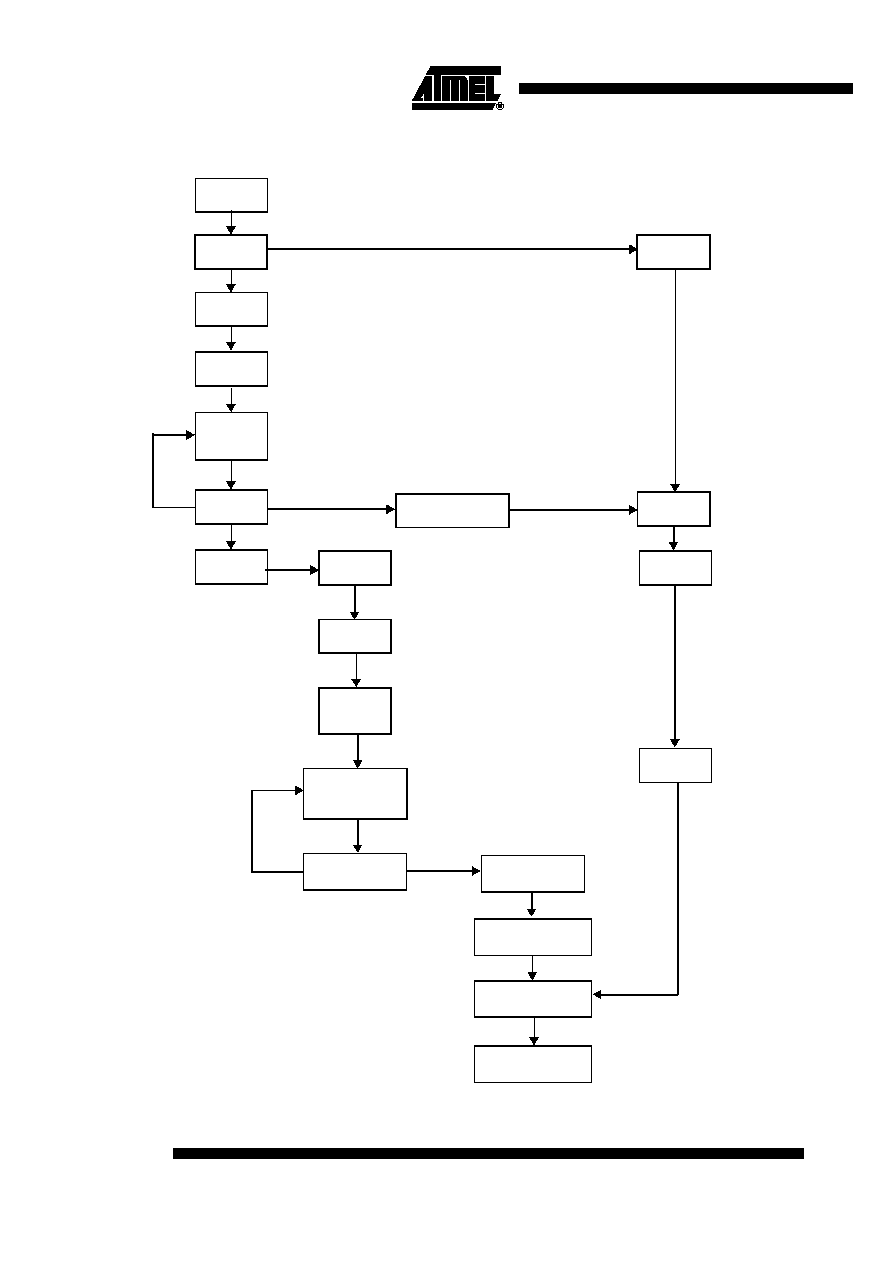
The Typical Gate Array/Embedded Array Design Flow, shown on page 4, provides a pic-
torial description of the typical interaction between Atmel's Gate Array/Embedded Array
design staff and the customer. Atmel will deliver design kits to support the customer's
synthesis, verification, floor planning, and SCAN insertion activities. Tools such as Syn-
opsys, Cadence, Verilog-HDL and CTgen are used, and many others are available.
Should a design include embedded memory or an embedded core, Atmel will support a
design review with the customer. The purpose of the design review is to permit Atmel to
understand the partition of the Gate Array/Embedded Array, and define the location of
the memory blocks and/or cores so that an underlayer layout model can be created.
Following a Preliminary Design Review, the design is routed, and post-route RC data is
extracted. Following post-route verification and a Final Design Review, the design is
taped out for fabrication.
4
MH1
4138E≠AERO≠06/02
Figure 1. Typical Gate Array/Embedded Array Design Flow
Deliver
Design Kit
Kickoff
Design
Synthesis
SCAN
Insertion
Functional
and Static
Path Sims
Floorplan
Database
Handoff
Database
Acceptance
Preliminary
Place and Route
Pre-route
Verification
Preliminary
Design
Review
Place and Route
and
Clock Tree
Post-route
Verification
Final
Design Review
Tape Out
Personality Layers
Fabricate
Personality
DVS
Assembly and Test
Create
Underlayer
Personality
Fabricate
Underlayer
Define
Underlayer
Atmel
Joint
Customer
Customer
Customer
Customer
Customer
Joint
Joint
Joint
Atmel
Joint
Logic
Joint
Atmel
Atmel
Atmel
Atmel
Atmel
Atmel
Joint
Embedded Array
5
MH1
4138E≠AERO≠06/02
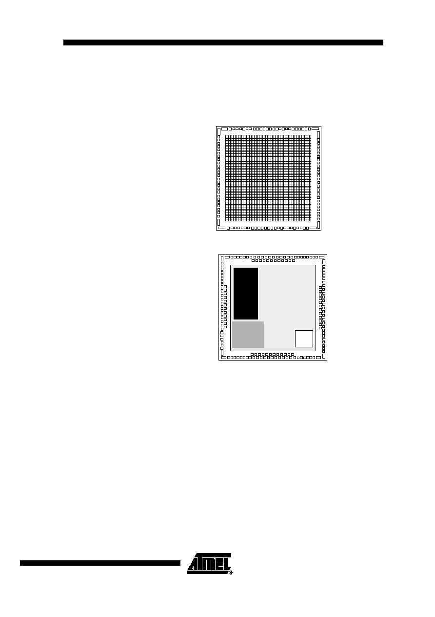
Pin Definition
Requirements
The corner pads are reserved for Power and Ground only. All other pads are fully pro-
grammable as Input, Output, Bidirectional, Power or Ground. When implementing a
design with 5V tolerant buffers, one buffer site must be reserved for the V
DD5
pin, which
is used to distribute power to the buffers.
Figure 1. Gate Array
Figure 2. Embedded Array
I/O Site: Pad and Sub-
Sections
The I/O sites can be configured as input, output, 3-state output and bidirectional buffers,
each with pull-up or pull-down capability, if required, by utilizing their corresponding sub-
section. Bidirectional buffers are the result of an input and output buffers placed in adja-
cent sub-sections in the same I/O site. Special buffers may require multiple I/O sites.
Oscillators require 2 I/O sites, each power and ground pin utilizes one I/O site.
PCI Buffers
PCI compatible input and output buffers are available for each bias voltage, 3V and 5V.
LVDS Buffers
Each LVDS buffer uses 2 I/O sites.
LVDS drivers are specific for each bias voltage and require one external current bias
resistor per chip; LVDS receiver is the same for all bias voltages and requires 1 external
line matching 100
resistor per receiver.
SRAM
ARM
RISC
Core
ROM
Standard
Gate Array
Architecture