 | –≠–ª–µ–∫—Ç—Ä–æ–Ω–Ω—ã–π –∫–æ–º–ø–æ–Ω–µ–Ω—Ç: SPI | –°–∫–∞—á–∞—Ç—å:  PDF PDF  ZIP ZIP |
1
Features
∑
Full-duplex, 3-wire Synchronous Data Transfer
∑
Master or Slave Operation
∑
Maximum Bit Frequency of f
CLOCK
/4 (in M-bits/second)
∑
LSB First or MSB First Data Transfer
∑
Four Programmable Bit Rates
∑
End of Transmission Interrupt Flag
∑
Write Collision Flag Protection
∑
Wakeup from Idle Mode (Slave Mode Only)
Description
The AVR
Æ
embedded RISC microcontroller core is a low-power, CMOS 8-bit micro-
processor based on the AVR enhanced RISC architecture. With this core, Atmel pro-
poses a Serial Peripheral Interace (SPI).
The SPI allows high-speed synchronous data transfers between the AVR core and
peripheral devices or between the AVR core and other cores.
Figure 1. SPI Pin Configuration
adr[5:0]
cp2
dbus_in[7:0]
iore
iowe
ireset
misoi
mosii
por
dbus_out[7:0]
misoo
mosio
out_en
scko
spe
SPI
scki
ss_b
test_se
test_si1
test_si2
spimaster
spirq
test_so1
test_so2
AVR Control
AVR Control
spiextload
spiload
spidwrite
spiack
SPI
Scan Test
IRQ
Slave
Programming
Mode
SPI
Scan Test
IRQ
Slave
Programming
Mode
Serial
Peripheral
Interface (SPI)
Embedded RISC
Microcontroller
Core Peripheral
Rev. 1127A≠10/99

SPI Core
2
P
Table 1. Pin Description
Pin Name
Description
Direction
Comments
AVR Control
cp2
CPU clock
Input
Any register in the SPI will update its contents only on the positive edge
of cp2
ireset
Synchronous reset
Input
When high, ireset will reset internal registers by reading the value on
dbus_in which is forced to zero by the AVR Core
dbus_out[7:
0]
Data bus output
Output
Valid only when accompanied by a strobe on out_en
dbus_in[7:0]
Data bus input
Input
out_en
Output enable strobe
Output
When high, out_en indicates that the SPI requires control of the data bus
adr[5:0]
I/O address inputs
Input
Valid only when accompanied by a strobe on iore or iowe
iore
I/O read strobe
Input
Used to read the contents of the I/O location addressed by adr
iowe
I/O write strobe
Input
Used to update the contents of the I/O location addressed by adr
SPI
ss_b
SPI slave select
Input
Used to select SPI activity, slave or master. If active, turns off the SPI
master flag (SPCR[4])
spe
SPI enable
Output
When high, spe indicates that the SPI peripheral is enabled. This mirrors
the spi enable flag (SPCR[6])
spimaster
SPI is master
Output
When high, indicates that SPI peripheral is in master mode. This mirrors
the SPI master flag (SPCR[4])
scko
SPI clock ouput
Output
Used to generate SPI clock in master mode
scki
SPI clock input
Input
Used to latch SPI data (MOSII and MISOO) in SPI slave mode
mosio
Master out, slave in output
Output
Used for data output in master mode
misoi
Master in, slave out input
Input
Used for data input in master mode
misoo
Master in, slave out output
Output
Used for data output in slave mode
mosii
Master out, slave in input
Input
Used for data input in slave mode
IRQ
spirq
SPI irq line
Output
When high, indicates that the SPI interrupt flag is set (SPSR[7]) and that
SPI interrupt is enabled (SPCR[7])
spiack
SPI interrupt acknowledge
Input
Used to reset SPI interrupt flag
Test Scan
test_se
Scan enable input
Input
Active high. Enable scan shift.
test_mode
Test mode input
Input
Active high. Must be set during scan testing.
test_si1
Scan chain 1 input
Input
Scan chain 1 input.
test_si2
Scan chain 2 input
Input
Scan chain 2 input.
test_so1
Scan chain 1 output
Output
Scan chain 1 input.
test_so2
Scan chain 2 output
Output
Scan chain 2 output.
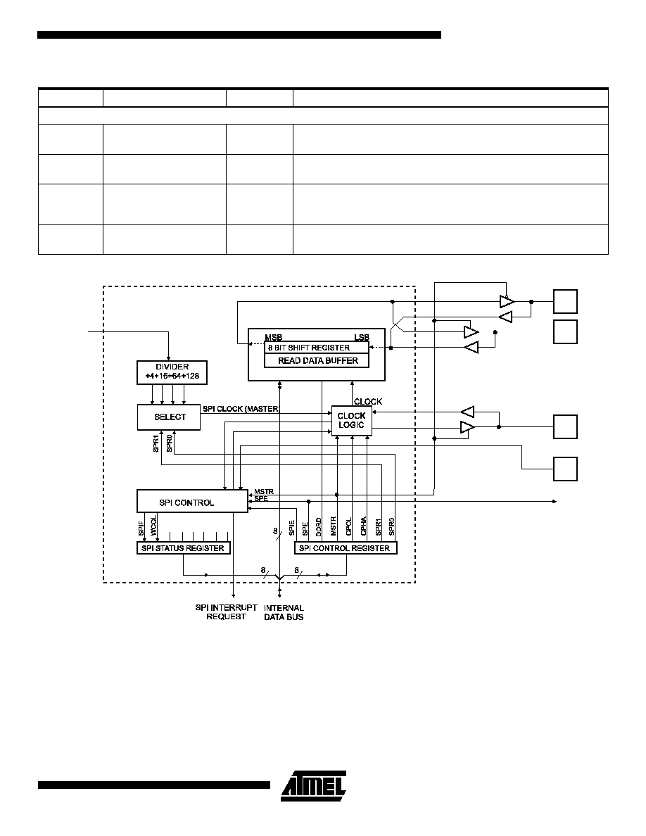
SPI Core
3
Figure 2. SPI Block Diagram
Slave Programming Mode
por
Power on reset
Input
Used to select SPI Flash/EEPROM programming slave mode. This
mode is enabled with por low and ireset high.
spiextload
External data load enable
Input
Enable parallel load of transmit shift register from dbus_in during slave
programming mode.
spiload
Active data load
Output
Indicates that the transmit shift register is updated on rising edge of cp2
with dbus_in value. This strobe will remain active until spiextload goes
low.
spidwrite
Active data write
Output
Indicates that a byte has been sent and data on dbus_out is valid for
reading.
Table 1. Pin Description (Continued)
Pin Name
Description
Direction
Comments
cp2
misoo
misoi
MISO
mosio
mosii
MOSI
spimaster
spe
SCK
scki
scko
SS
ss_b

SPI Core
4
Description
The SPI is a fully synchronous peripheral. It can run at a
F
C P 2
/4 m a x im u m b a u d ra t e w h i c h i s c o n t ro l l e d b y
SPCR[1:0].
The SPI has one interrupt request output called spirq. This
interrupt is controlled as follows:
∑ Cleared by ireset
∑ Set when receive FIFO is full
∑ Cleared by acknowledge (spiack high)
∑ Cleared by a read in the SPI Status Register (SPSR)
followed by an access to SPI Data Register (SPDR),
read or write
The interconnection between master and slave CPUs with
SPI is shown in Figure 3. The SCK pin is the clock output in
the master mode and is the clock input in the slave mode.
Writing to the SPI data register of the master CPU starts
the SPI clock generator, and the data written shifts out of
the MOSI pin and into the MOSI pin of the slave CPU. After
shifting one byte, the SPI clock generator stops, setting the
end of transmission flag (SPIF). If the SPI interrupt enable
bit (SPIE) in the SPCR register becomes set, an interrupt is
requested. The Slave Select input, SS, is set low to select
an individual SPI device as a slave. The two shift registers
in the Master and the Slave can be considered as one dis-
tributed 16-bit circular shift register. This is shown in Figure
3. When data is shifted from the master to the slave, data is
also shifted in the opposite direction simultaneously. This
means that during one shift cycle, data in the master and
the slave are interchanged.
Figure 3. SPI Master-Slave Interconnection
The system is single buffered in the transmit direction and
double buffered in the receive direction. This means that
characters to be transmitted cannot be written to the SPI
Data Register before the entire shift cycle is completed.
When receiving data, however, a received character must
be read from the SPI Data Register before the next charac-
ter has been completely shifted in. Otherwise, the first char-
acter is lost.
When the SPI is enabled, the data direction of the MOSI,
MISO, SCK and SS pins is overriden according to the fol-
lowing table:
Table 2. SPI Pin Overrides
Pin
Direction, Master SPI
Direction, Slave SPI
MOSI
Output
Input
MISO
Input
Output
SCK
Output
Input
SS
≠
Input
SPI Core
5
SS Pin Functionality
When the SPI is configured as a master (MSTR in SPCR is
set), the user can determine the direction of the SS pin. If
SS is configured as an output, the pin is a general output
pin which does not affect the SPI system. If SS is config-
ured as an input, it must be held high to ensure Master SPI
operation. If, in master mode, the SS pin is input, and is
driven low by peripheral circuitry, the SPI system interprets
this as that another master selects the SPI as a slave and
will start sending data to it. To avoid bus contention, the
SPI system takes the following actions:
1. The MSTR bit in SPCR is cleared and the SPI system
becomes a slave. As a result of the SPI becoming a
slave, the MOSI and SCK pins become inputs.
2. The SPIF flag in SPSR is set, and if the SPI interrupt is
enabled, the interrupt routine will be executed.
Thus, when interrupt-driven SPI transmision is used in
master mode, and there is a possibility that SS is driven
low, the interrupt should always check that the MSTR bit is
still set. Once the MSTR bit has been cleared by a slave
select, it must be set by the user.
When the SPI is configured as a slave, the SS is always
input. When SS is held low, the SPI is activated and MISO
becomes an output if configured so by the user. All other
pins are inputs. When SS is driven low, all pins are inputs,
and the SPI is passive, which means that it will not receive
incoming data.
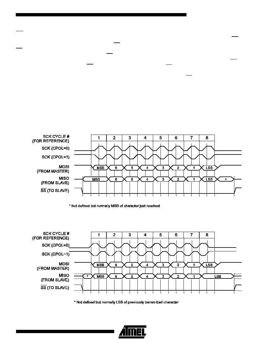
Data Modes
There are four combinations of SCK phase and polarity
with respect to serial data, which are determined by control
bits CPHA and CPOL. The SPI data transfer formats are
shown in Figure 4 and Figure 5.
Figure 4. SPI Transfer Format with CPHA = 0
Figure 5. SPI Transfer Format with CPHA = 1