1
Features
∑
1024 x 1024 Pixels with Memory Zone
∑
Up to 30 Images/Second
∑
Built-in Antiblooming Device Providing an Electric Shutter Function
∑
Pixel: 14 µm x 14 µm
∑
Image Zone: 14.34 x 14.34 mm
2
∑
Two Outputs at 20 MHz Each
∑
Readout Through 1 or 2 Outputs
∑
Possible Binning 2 x 2
∑
Optical Shield Against Parasitic Reflexions and Stray Light
∑
A/R Window in 400 - 700 nm Bandwidth
Description
The TH7888A is particularly designed for high data rate applications (up to 30 pic-
tures/second in 1024 x 1024 progressive scan format) in the medical and industrial
fields. This area array image sensor consists of a 1024 x 1024 pixels (14 µm x 14 µm)
image zone associated with a memory zone (masked with an optical shield). To
increase the data rate, two separate outputs are provided, which can be used for par-
allel readout (the readout frequency is up to 20 MHz/output, leading to a total readout
frequency of 40 MHz). These two outputs allow three readout modes (single or dual
port). The TH7888A is designed with an antiblooming structure which provides an
electronic shutter capability. Moreover, the 2 x 2 binning mode is available on this sen-
sor, providing an image size of 512 x 512 pixels with 28 µm x 28 µm pixels. The
TH7888A package is sealed with a specific anti-reflective window optimized in the 400
- 700 nm spectrum bandwidth on the sealed version.
Area Array CCD
Image Sensor
(1024 x 1024
Pixels with
Antiblooming)
TH7888A
Rev. 1999A≠IMAGE≠09/03

2
TH7888A
1999A≠IMAGE≠09/03
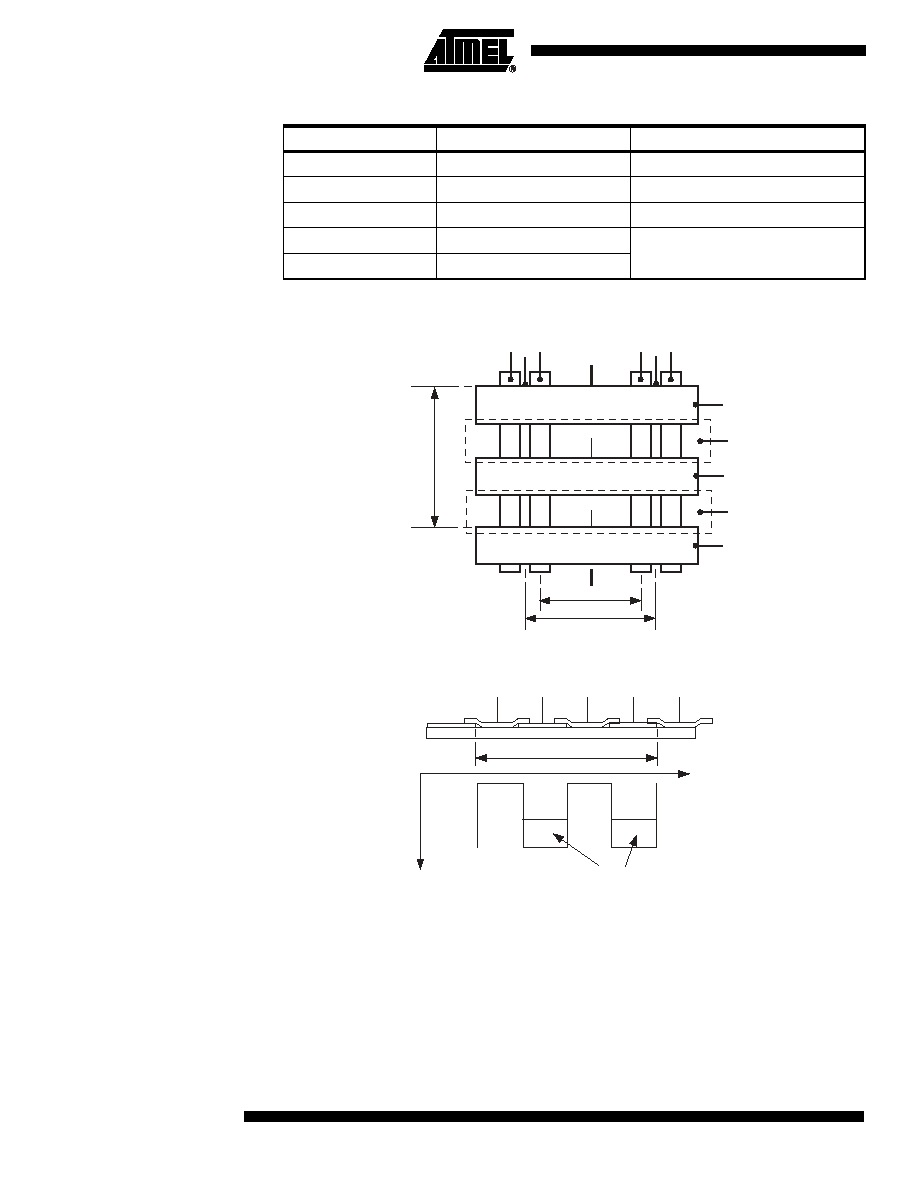
Figure 1. TH7888A General Sensor Organization
Functional Overview
Extra dark lines are provided for use as dark references or for smearing digital correc-
tion.
Extra dark pixels are provided for dark line reference clamping. Each frame consists of
1056 video lines:
∑
1 dummy line
∑
12 useful dark reference lines (with optical shield)
∑
3 isolation lines
∑
1024 useful lines
∑
3 isolation lines
∑
12 dark reference lines (with optical shield)
∑
1 dummy line
Each video line is made up of 546 or 1058 elements, depending on the readout mode
(single or dual port mode):
∑
12 inactive prescan elements
∑
1 isolation prescan element
∑
16 useful dark references (with optical shield)
∑
5 isolation elements
∑
512 or 1024 useful video pixels
1024 x 1024
Image Area
1024 x 1024
Memory Area
P1,2,3,4
M1,2,3,4
A
R
L1-6
VA
M
R
VDR
VDD2
VOS2
VS2
VGS
VDR
VDD1
VOS1
VS1
VGS
Bi-directional Serial Register

5
TH7888A
1999A≠IMAGE≠09/03
Absolute Maximum Ratings*
Operating Precautions
Shorting the video outputs to any pin, even temporarily, can permanently damage the
on-chip output amplifier.
Storage Temperature ..................................... -55∞C to +150∞C
*NOTICE:
*Stresses above those listed under absolute
maximum ratings may cause permanent device
failure. Functionality at or above these limits is
not implied. Exposure to absolute maximum rat-
ings for extended periods may affect device reli-
ability. Operating range defines the limits within
which functionality is guaranteed. Electrical limits
of applied signals are given in the operating con-
ditions section.
Operating Temperature.................................... -40∞C to +85∞C
Thermal Cycling..........................................................15∞C/mn
Maximum Applied Voltages:
∑ Pins: Y9, AA9, Y10, AA10, Y5, AA5, Y6,
AA6, Y4, B2, A2, A3, B3, B1, A1, B4, A6 ...........-0.3 V to 15 V
∑ Pins: A9, A8, B10, B8, B7, A7, AA7 ..............-0.3 V to 15.5 V
∑ Pin: Y7..............................................................-0.3 V to 12 V
∑ Pins: A4, A5, B5, B6, Y8, AA4, AA8 ................... 0 V (ground)