1
Features
∑
CPU32+ Processor (4.5 MIPS at 25 MHz)
≠ 32-bit Version of the CPU32 Core (Fully Compatible with the CPU32)
≠ Background Debug Mode
≠ Byte-misaligned Addressing
∑
Up to 32-bit Data Bus (Dynamic Bus Sizing for 8 and 16 Bits)
∑
Up to 32 Address Lines (At Least 28 Always Available)
∑
Complete Static Design (0 - 25 MHz Operation)
∑
Slave Mode to Disable CPU32+ (Allows Use with External Processors)
≠ Multiple QUICCs Can Share One System Bus (One Master)
≠ TS68040 Companion Mode Allows QUICC to be a TS68040 Companion Chip and
Intelligent Peripheral (22 MIPS at 25 MHz)
≠ Peripheral Device of TSPC603e (see DC415/D note)
∑
Four General-purpose Timers
≠ Superset of MC68302 Timers
≠ Four 16-bit Timers or Two 32-bit Timers
≠ Gate Mode Can Enable/Disable Counting
∑
Two Independent DMAs (IDMAs)
∑
System Integration Module (SIM60)
∑
Communications Processor Module (CPM)
∑
Four Baud Rate Generators
∑
Four SCCs (Ethernet/IEEE 802.3 Optional on SCC1-Full 10 Mbps Support)
∑
Two SMC
∑
V
CC
= +5V Ī 5%
∑
f
max
= 25 MHz and 33 MHz
∑
Military Temperature Range: -55
į
C < T
C
< +125
į
C
∑
P
D
= 1.4 W at 25 MHz; 5.25V
2 W at 33 MHz; 5.25V
Description
The TS68EN360 QUad Integrated Communication Controller (QUICC
TM
) is a versatile
one-chip integrated microprocessor and peripheral combination that can be used in a
variety of controller applications. It particularly excels in communications activities.
The QUICC (pronounced "quick") can be described as a next-generation TS68302
with higher performance in all areas of device operation, increased flexibility, major
extensions in capability, and higher integration. The term "quad" comes from the fact
that there are four serial communications controllers (SCCs) on the device; however,
there are actually seven serial channels: four SCCs, two serial management control-
lers (SMCs), and one serial peripheral interface (SPI).
Screening/Quality
This product is manufactured in full compliance with:
∑
MIL-STD-883 (class B)
∑
QML (class Q)
∑
or according to Atmel standards
32-bit Quad
Integrated
Communication
Controller
TS68EN360
Rev. 2113A≠HIREL≠03/02
2
TS68EN360
2113A≠HIREL≠03/02
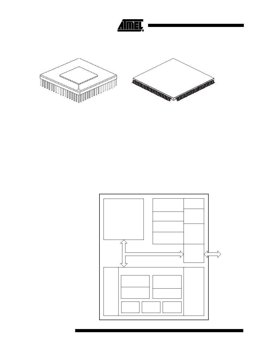
Introduction
QUICC Architecture
Overview
The QUICC is 32-bit controller that is an extension of other members of the TS68300
family. Like other members of the TS68300 family, the QUICC incorporates the inter-
module bus (IMB). The TS68302 is an exception, having an 68000 bus on chip. The IMB
provides a common interface for all modules of the TS68300 family, which allows the
development of new devices more quickly by using the library of existing modules.
Although the IMB definition always included an option for an on-chip 32-bit bus, the
QUICC is the first device to implement this option.
The QUICC is comprised of three modules: the CPU32+ core, the SIM60, and the CPM.
Each module utilizes the 32-bit IMB.
The TS68EN360 QUICC block diagram is shown in Figure 1.
Figure 1. QUICC Block Diagram
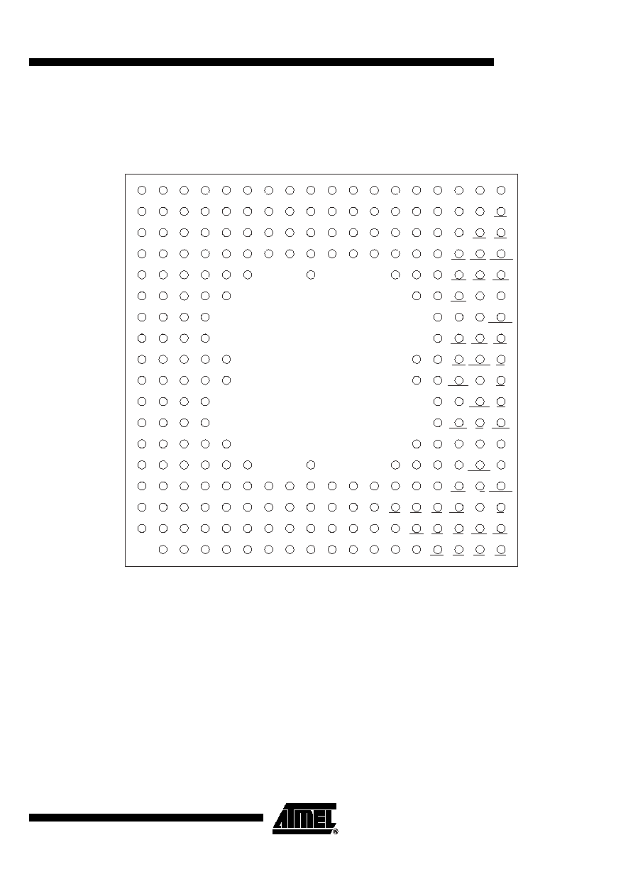
R suffix
PGA 241
Ceramic Pin Grid Array Cavity Up
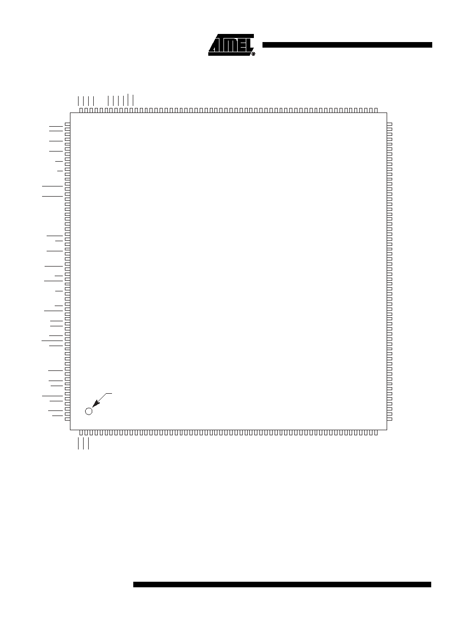
A suffix
CERQUAD 240
Ceramic Leaded Chip Carrier Cavity Down
EXTERNAL
BUS
INTERFACE
SYSTEM
PROTECTION
SIM 60
CPU32+
CORE
IMB (32 BIT)
RISC
CONTROLLER
SYSTEM
I/F
2.5-KBYTE
DUAL-PORT
RAM
DRAM
CONTROLLER
AND
CHIP SELECTS
CPM
PERIODIC
TIMER
CLOCK
GENERATION
OTHER
FEATURES
BREAKPOINT
LOGIC
JTAG
COMMUNICATIONS PROCESSOR
FOUR
GENERAL-
PURPOSE
TIMERS
INTERRUPT
CONTROLLER
OTHER
FEATURES
TIMER SLOT
ASSIGNER
SEVEN
SERIAL
CHANNELS
TWO
IDMAs
FOURTEEN SERIAL
DMAs
5
TS68EN360
2113A≠HIREL≠03/02
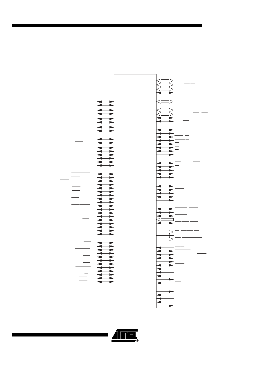
Signal Description
Functional Signal Group
Figure 4. QUICC Functional Signal Groups
QUICC
A31ĪA28/WE0ĪWE3
A27ĪA0
DATA BUS
D31ĪD16
D15ĪD0
PRTY3/16BM
BUS CONTROL
SIZ0
SIZ1
R/W
AS
BUS ARBITRATION
BR
BG
BCLRO/CONFIG1/RAS2DD
SYSTEM CONTROL
RESETH
RESETS
HALT
PERR
INTERRUPT CONTROL
AVEC/IACK5/AVECO
MEMORY CONTROLLER
CS6ĪCS0/RAS6ĪRAS0
CS/RAS7/IACK7
CAS3ĪCAS0/IACK6,3,2,1
TCK
TMS
TDI
TDO
TRST
CLOCK
XTAL
EXTAL
XFC
MODCK1ĪMODCK0
CLKO2ĪCLKO1
ADDRESS BUS
RXD1/PA0
PORT A
TXD1/PA1
RXD2/PA2
TXD2/PA3
L1TXDB/RXD3/PA4
L1RXDB/TXD3/PA5
L1TXDA/RXD4/PA6
L1RXDA/TXD4/PA7
TIMERs/SCCs/SIs/CLOCKs/BRG
TIN1/L1RCLKA/BRGO1/CLK1/PA8
BRGCLK1/TOUT1/CLK2/PA9
TIN2/L1TCLKA/BRGO2/CLK3/PA10
TOUT2/CLK4/PA11
TIN3/BRGO3/CLK5/PA12
BRGCLK2/L1RCLKB/TOUT3/CLK6/PA13
TIN4/BRGO4/CLK7/PA14
L1TCLKB/TOUT4/CLK8/PA15
PORT B (PIP)
RRJCT1/SPISEL/PB0
RSTRT2/SPICLK/PB1
RRJCT2/SPIMOSI(SPITXD)/PB2
BRGO4/SPIMISO(SPIRXD)/PB3
DREQ1/BRGO1/PB4
DACK1/BRGO2/PB5
DONE1/SMTXD1/PB6
DONE2/SMRXD1/PB7
DREQ2/SMSYN1/PB8
DACK2/SMSYN2/PB9
L1CLKOB/SMTXD2/PB10
L1CLKOA/SMRXD2/PB11
L1ST1/RTS1/PB12
L1ST2/RTS2/PB13
L1ST3/L1RQB/RTS3/PB14
L1ST4/L1RQA/RTS4/PB15
STRBO/BRGO3/PB16
STRBI/RSTRT1/PB17
PORT C (INTERRUPT PARALLEL I/O)
L1ST1/RTS1/PC0
L1ST2/RTS2/PC1
L1ST3/L1RQB/RTS3/PC2
L1ST4/L1RQA/RTS4/PC3
CTS1/PC4
TGATE1/CD1/PC5
CTS2/PC6
TGATE2/CD2/PC7
SDACK2/L1TSYNCB/CTS3/PC8
L1RSYNCB/CD3/PC9
SDACK1/L1TSYNCA/CTS4/PC10
L1RSYNCA/CD4/PC11
TS68360
240 PINS
TEST
FC2ĪFC0/
TM2ĪTM0
FC3/
TT0
PRTY1ĪPRTY2/
IOUT1ĪIOUT2
PRTY2/IOUT0/
RQOUT
DSACK0/
TBI
DSACK1/
TA
DS/
TT1
OE/AMUX
RMC/CONFIG0/
LOCK
BGACK/
BB
BERR/
TEA
IRQ1/
OUT0/RQOUT
IRQ1/
OUT0/RQOUT
IRQ4/
OUT1
IRQ6/
OUT2
IRQ2,3,5,7
TRIS/
TS
BKPT/
BKPT0/DSCLK
FREEZE/CONFIG2/
MBARE
IPIPE1/RAS1DD/
BCLRI
IPIPE0/
BADD2/DSO
IFETCH/
BADD3/DSI