Rev. C - 15 January, 2001
1
TS80C54X2/C58X2
TS87C54X2/C58X2
8-bit CMOS Microcontroller 16/32 Kbytes ROM/OTP
1. Description
TS80C54/58X2 is high performance CMOS ROM, OTP
and EPROM versions of the 80C51 CMOS single chip
8-bit microcontroller.
The TS80C54/58X2 retains all features of the Atmel
Wireless & Microcontrollers
80C51 with extended
ROM/EPROM capacity (16/32 Kbytes), 256 bytes of
internal RAM, a 6-source , 4-level interrupt system, an
on-chip oscilator and three timer/counters.
In addition, the TS80C54/58X2 has a Hardware
Watchdog Timer, a more versatile serial channel that
facilitates multiprocessor communication (EUART) and
a X2 speed improvement mechanism.
The fully static design of the TS80C54/58X2 allows to
reduce system power consumption by bringing the clock
frequency down to any value, even DC, without loss of
data.
The TS80C54/58X2 has 2 software-selectable modes of
reduced
activity
for
further
reduction
in
power
consumption. In the idle mode the CPU is frozen while
the timers, the serial port and the interrupt system are still
operating. In the power-down mode the RAM is saved
and all other functions are inoperative.
2. Features
q
80C52 Compatible
�
8051 pin and instruction compatible
�
Four 8-bit I/O ports
�
Three 16-bit timer/counters
�
256 bytes scratchpad RAM
q
High-Speed Architecture
�
40 MHz @ 5V, 30MHz @ 3V
�
X2 Speed Improvement capability (6 clocks/
machine cycle)
30 MHz @ 5V, 20 MHz @ 3V (Equivalent to
60 MHz @ 5V, 40 MHz @ 3V)
q
Dual Data Pointer
q
On-chip ROM/EPROM (16K-bytes, 32K-bytes)
q
Programmable Clock Out and Up/Down Timer/
Counter 2
q
Hardware Watchdog Timer (One-time enabled with
Reset-Out)
q
Asynchronous port reset
q
Interrupt Structure with
�
6 Interrupt sources
�
4 level priority interrupt system
q
Full duplex Enhanced UART
�
Framing error detection
�
Automatic address recognition
q
Low EMI (inhibit ALE)
q
Power Control modes
�
Idle mode
�
Power-down mode
�
Power-off Flag
q
Once mode (On-chip Emulation)
q
Power supply: 4.5-5.5V, 2.7-5.5V
q
Temperature ranges: Commercial (0 to 70
o
C) and
Industrial (-40 to 85
o
C)
q
Packages: PDIL40, PLCC44, VQFP44 1.4, PQFP44
F1, CQPJ44 (window), CDIL40 (window)
Rev. C - 15 January, 2001
3
TS80C54X2/C58X2
TS87C54X2/C58X2
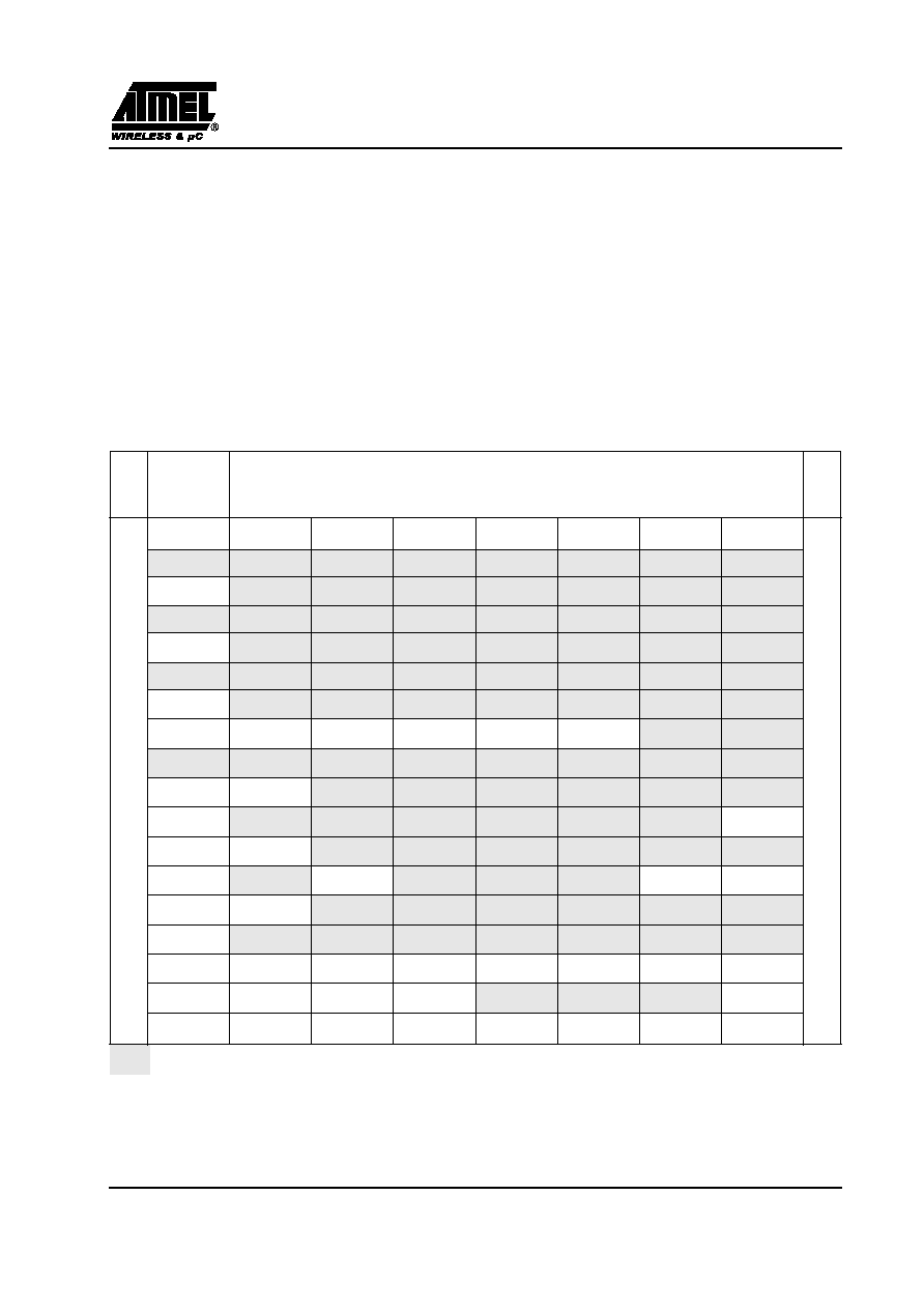
4. SFR Mapping
The Special Function Registers (SFRs) of the TS80C54/58X2 fall into the following categories:
�
C51 core registers: ACC, B, DPH, DPL, PSW, SP, AUXR1
�
I/O port registers: P0, P1, P2, P3
�
Timer registers: T2CON, T2MOD, TCON, TH0, TH1, TH2, TMOD, TL0, TL1, TL2, RCAP2L, RCAP2H
�
Serial I/O port registers: SADDR, SADEN, SBUF, SCON
�
Power and clock control registers: PCON
�
HDW Watchdog Timer Reset: WDTRST, WDTPRG
�
Interrupt system registers: IE, IP, IPH
�
Others: AUXR, CKCON
Table 2. All SFRs with their address and their reset value
Bit
address-
able
Non Bit addressable
0/8
1/9
2/A
3/B
4/C
5/D
6/E
7/F
F8h
FFh
F0h
B
0000 0000
F7h
E8h
EFh
E0h
ACC
0000 0000
E7h
D8h
DFh
D0h
PSW
0000 0000
D7h
C8h
T2CON
0000 0000
T2MOD
XXXX XX00
RCAP2L
0000 0000
RCAP2H
0000 0000
TL2
0000 0000
TH2
0000 0000
CFh
C0h
C7h
B8h
IP
XX00 0000
SADEN
0000 0000
BFh
B0h
P3
1111 1111
IPH
XX00 0000
B7h
A8h
IE
0X00 0000
SADDR
0000 0000
AFh
A0h
P2
1111 1111
AUXR1
XXXX 0XX0
WDTRST
XXXX XXXX
WDTPRG
XXXX X000
A7h
98h
SCON
0000 0000
SBUF
XXXX XXXX
9Fh
90h
P1
1111 1111
97h
88h
TCON
0000 0000
TMOD
0000 0000
TL0
0000 0000
TL1
0000 0000
TH0
0000 0000
TH1
0000 0000
AUXR
XXXX XX00
CKCON
XXXX XXX0
8Fh
80h
P0
1111 1111
SP
0000 0111
DPL
0000 0000
DPH
0000 0000
PCON
00X1 0000
87h
0/8
1/9
2/A
3/B
4/C
5/D
6/E
7/F
reserved
Rev. C - 15 January, 2001
5
TS80C54X2/C58X2
TS87C54X2/C58X2
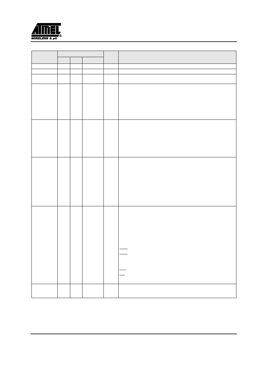
Table 3. Pin Description for 40/44 pin packages
MNEMONIC
PIN NUMBER
TYPE
NAME AND FUNCTION
DIL
LCC
VQFP 1.4
V
SS
20
22
16
I
Ground: 0V reference
Vss1
1
39
I
Optional Ground: Contact the Sales Office for ground connection.
V
CC
40
44
38
I
Power Supply: This is the power supply voltage for normal, idle and power-
down operation
P0.0-P0.7
39-32
43-36
37-30
I/O
Port 0: Port 0 is an open-drain, bidirectional I/O port. Port 0 pins that have 1s
written to them float and can be used as high impedance inputs. Port 0 pins must
be polarized to Vcc or Vss in order to prevent any parasitic current consumption.
Port 0 is also the multiplexed low-order address and data bus during access to
external program and data memory. In this application, it uses strong internal
pull-up when emitting 1s. Port 0 also inputs the code bytes during EPROM
programming. External pull-ups are required during program verification during
which P0 outputs the code bytes.
P1.0-P1.7
1-8
2-9
40-44
1-3
I/O
Port 1: Port 1 is an 8-bit bidirectional I/O port with internal pull-ups. Port 1
pins that have 1s written to them are pulled high by the internal pull-ups and
can be used as inputs. As inputs, Port 1 pins that are externally pulled low will
source current because of the internal pull-ups. Port 1 also receives the low-order
address byte during memory programming and verification.
Alternate functions for Port 1 include:
1
2
40
I/O
T2 (P1.0): Timer/Counter 2 external count input/Clockout
2
3
41
I
T2EX (P1.1): Timer/Counter 2 Reload/Capture/Direction Control
P2.0-P2.7
21-28
24-31
18-25
I/O
Port 2: Port 2 is an 8-bit bidirectional I/O port with internal pull-ups. Port 2
pins that have 1s written to them are pulled high by the internal pull-ups and
can be used as inputs. As inputs, Port 2 pins that are externally pulled low will
source current because of the internal pull-ups. Port 2 emits the high-order address
byte during fetches from external program memory and during accesses to external
data memory that use 16-bit addresses (MOVX @DPTR).In this application, it
uses strong internal pull-ups emitting 1s. During accesses to external data memory
that use 8-bit addresses (MOVX @Ri), port 2 emits the contents of the P2 SFR.
Some Port 2 pins receive the high order address bits during EPROM programming
and verification:
P2.0 to P2.5 for A8 to A13
P3.0-P3.7
10-17
11,
13-19
5,
7-13
I/O
Port 3: Port 3 is an 8-bit bidirectional I/O port with internal pull-ups. Port 3
pins that have 1s written to them are pulled high by the internal pull-ups and
can be used as inputs. As inputs, Port 3 pins that are externally pulled low will
source current because of the internal pull-ups. Some Port 3 pin P3.4 receive
the high order address bits during EPROM programming and verification for
TS8xC58X2 devices.
Port 3 also serves the special features of the 80C51 family, as listed below.
10
11
5
I
RXD (P3.0): Serial input port
11
13
7
O
TXD (P3.1): Serial output port
12
14
8
I
INT0 (P3.2): External interrupt 0
13
15
9
I
INT1 (P3.3): External interrupt 1
14
16
10
I
T0 (P3.4): Timer 0 external input
15
17
11
I
T1 (P3.5): Timer 1 external input
16
18
12
O
WR (P3.6): External data memory write strobe
17
19
13
O
RD (P3.7): External data memory read strobe
P3.4 also receives A14 during TS87C58X2 EPROM Programming.
Reset
9
10
4
I
Reset: A high on this pin for two machine cycles while the oscillator is running,
resets the device. An internal diffused resistor to V
SS
permits a power-on reset
using only an external capacitor to V
CC.