 | ÐлекÑÑоннÑй компоненÑ: ISO120 | СкаÑаÑÑ:  PDF PDF  ZIP ZIP |
Äîêóìåíòàöèÿ è îïèñàíèÿ www.docs.chipfind.ru
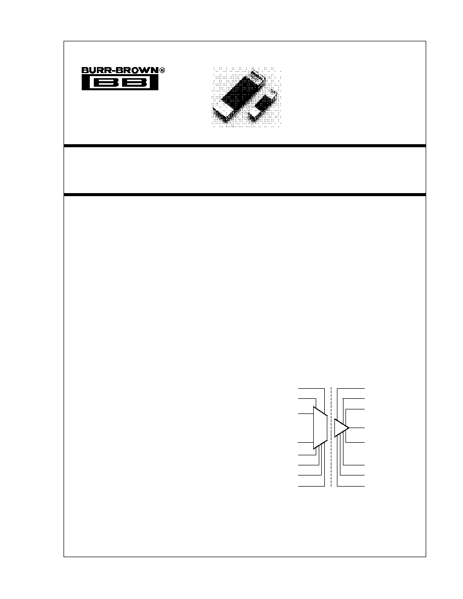
Precision Low Cost
ISOLATION AMPLIFIER
ISO120
ISO121
Signal
Com 2
V
S2
Gnd 2
+V
S2
Ext Osc
+V
S1
Gnd 1
V
S1
Signal
Com 1
V
OUT
C
1L
C
1H
Sense
C
2L
C
2H
Isolation Barrier
V
IN
DESCRIPTION
The ISO120 and ISO121 are precision isolation ampli-
fiers incorporating a novel duty cycle modulation-
demodulation technique. The signal is transmitted
digitally across a 2pF differential capacitive barrier.
With digital modulation the barrier characteristics do
not affect signal integrity, which results in excellent
reliability and good high frequency transient immu-
nity across the barrier. Both the amplifier and barrier
capacitors are housed in a hermetic DIP. The ISO120
and ISO121 differ only in package size and isolation
voltage rating.
These amplifiers are easy to use. No external compo-
nents are required for 60kHz bandwidth. With the
addition of two external capacitors, precision specifi-
cations of 0.01% max nonlinearity and 150
µ
V/
°
C max
V
OS
drift are guaranteed with 6kHz bandwidth. A
power supply range of
±
4.5V to
±
18V and low quies-
cent current make these amplifiers ideal for a wide
range of applications.
FEATURES
q
100% TESTED FOR PARTIAL DISCHARGE
q
ISO120: Rated 1500Vrms
q
ISO121: Rated 3500Vrms
q
HIGH IMR: 115dB at 60Hz
q
USER CONTROL OF CARRIER
FREQUENCY
q
LOW NONLINEARITY:
±
0.01% max
q
BIPOLAR OPERATION: V
O
=
±
10V
q
0.3"-WIDE 24-PIN HERMETIC DIP, ISO120
q
SYNCHRONIZATION CAPABILITY
q
WIDE TEMP RANGE: 55
°
C to +125
°
C
(ISO120)
APPLICATIONS
q
INDUSTRIAL PROCESS CONTROL: Trans-
ducer Isolator for Thermocouples, RTDs,
Pressure Bridges, and Flow Meters, 4mA
to 20mA Loop Isolation
q
GROUND LOOP ELIMINATION
q
MOTOR AND SCR CONTROL
q
POWER MONITORING
q
ANALYTICAL MEASUREMENTS
q
BIOMEDICAL MEASUREMENTS
q
DATA ACQUISITION
q
TEST EQUIPMENT
International Airport Industrial Park · Mailing Address: PO Box 11400 · Tucson, AZ 85734 · Street Address: 6730 S. Tucson Blvd. · Tucson, AZ 85706
Tel: (520) 746-1111 · Twx: 910-952-1111 · Cable: BBRCORP · Telex: 066-6491 · FAX: (520) 889-1510 · Immediate Product Info: (800) 548-6132
© 1988 Burr-Brown Corporation
PDS-820D
Printed in U.S.A. March, 1992
SBOS158

2
ISO120/121
SPECIFICATIONS
ELECTRICAL
At T
A
= +25
°
C: V
S1
= V
S2
=
±
15V: and R
L
= 2k
, unless otherwise noted.
*Specifications same as ISO120BG, ISO121BG.
NOTE: (1) Input voltage range =
±
10V for V
S1
, V
S2
=
±
4.5VDC to
±
18VDC. (2) Ripple frequency is at carrier frequency. (3) Overload recovery is approximately three times
the settling time for other values of C
2
. (4) The SG-grade is specified 55
°
C to +125
°
C; performance of the SG in the 25
°
C to +85
°
C temperature range is the same
as the BG-grade.
ISO120BG, ISO121BG ISO120G, ISO120SG
(4)
, ISO121G
PARAMETER
CONDITIONS
MIN
TYP
MAX
MIN
TYP
MAX
UNITS
ISOLATION
Voltage Rated Continuous ISO120: AC 60Hz
T
MIN
to T
MAX
1500
*
Vrms
DC
T
MIN
to T
MAX
2121
*
VDC
ISO121: AC 60Hz
T
MIN
to T
MAX
3500
*
Vrms
DC
T
MIN
to T
MAX
4950
*
VDC
100% Test (AC 60Hz): ISO120
1s; Partial Discharge
5pC
2500
*
Vrms
ISO121
1s; Partial Discharge
5pC
5600
*
Vrms
Isolation Mode Rejection ISO 120: AC 60Hz
1500Vrms
115
*
dB
DC
160
*
dB
ISO121: AC60Hz
3500Vrms
115
*
dB
DC
160
*
dB
Barrier Impedance
10
14
|| 2
*
|| pF
Leakage Current
V
ISO
= 240Vrms, 60Hz
0.18
0.5
*
*
µ
Arms
GAIN
(4)
V
O
=
±
10V
Nominal Gain
C
1
= C
2
= 1000pF
1
1
V/V
Gain Error
±
0.04
±
0.1
±
0.05
±
0.25
%FSR
Gain vs Temperature
±
5
±
20
±
10
±
40
ppm/
°
C
Nonlinearity
±
0.005
±
0.01
±
0.01
±
0.05
%FSR
Nominal Gain
C
1
= C
2
= 0
1
1
V/V
Gain Error
±
0.04
±
0.25
±
0.05
±
0.25
%FSR
Gain vs Temperature
±
40
±
40
ppm/
°
C
Nonlinearity
±
0.02
±
0.1
±
0.04
±
0.1
%FSR
INPUT OFFSET VOLTAGE
(4)
Initial Offset
C
1
= C
2
= 1000pF
±
5
±
25
±
10
±
50
mV
vs Temperature
±
100
±
150
±
150
±
400
µ
V/
°
C
Initial Offset
C
1
= C
2
= 0
±
25
±
100
±
40
±
100
mV
vs Temperature
±
250
±
500
µ
V/
°
C
Initial Offset
vs Supply
±
V
S1
or
±
V
S2
=
±
4.5V to
±
18V
±
2
±
2
mV/V
Noise
4
4
µ
V/
Hz
INPUT
Voltage Range
(1)
±
10
±
15
*
*
V
Resistance
200
*
k
OUTPUT
Voltage Range
±
10
±
12.5
*
*
V
Current Drive
±
5
±
15
*
*
mA
Capacitive Load Drive
0.1
*
µ
F
Ripple Voltage
(2)
10
*
mVp-p
FREQUENCY RESPONSE
Small Signal Bandwith
C
1
= C
2
= 0
60
*
kHz
C
1
= C
2
= 1000pF
6
*
kHz
Slew Rate
2
*
V/
µ
s
Settling Time
V
O
=
±
10V
0.1%
C
2
= 100pF
50
*
µ
s
0.01%
C
1
= C
2
= 1000pF
350
*
µ
s
Overload Recovery Time
(3)
50% Output Overload,
150
*
µ
s
C
1
= C
2
= 0
POWER SUPPLIES
Rated Voltage
15
*
V
Voltage Range
±
4.5
±
18
*
*
V
Quiescent Current: V
S1
±
4.0
±
5.5
*
*
mA
V
S2
±
5.0
±
6.5
*
*
mA
TEMPERATURE RANGE
Specification: BG and G
25
85
25
85
°
C
SG
(4)
25
85
55
125
°
C
Operating
55
125
55
125
°
C
Storage
65
150
55
150
°
C
JA
: ISO120
40
40
°
C/W
ISO121
25
25
°
C/W
3
ISO120/121
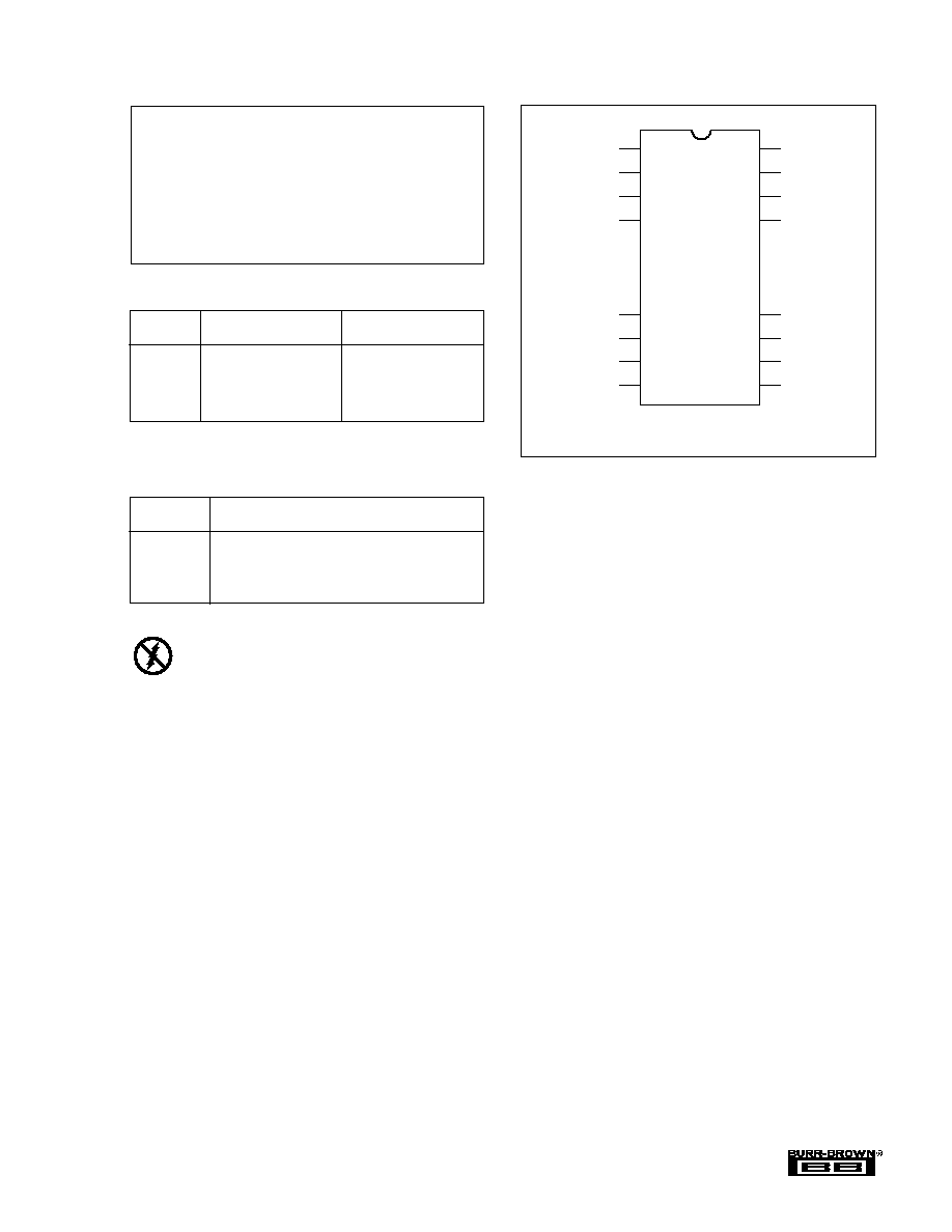
PACKAGE DRAWING
MODEL
PACKAGE
NUMBER
ISO120G
24-Pin DIP
225
ISO120BG
24-Pin DIP
225
ISO120SG
24-Pin DIP
225
ISO121G
40-Pin DIP
206
ISO121BG
40-Pin DIP
206
NOTE: (1) For detailed drawing and dimension table, please see end of data
sheet, or Appendix D of Burr-Brown IC Data Book.
ABSOLUTE MAXIMUM RATINGS
CONNECTION DIAGRAM
Supply Voltage (any supply) ............................................................... 18V
V
IN
, Sense Voltage ..........................................................................
±
100V
External Oscillator Input ....................................................................
±
25V
Signal Common 1 to Ground 1 ...........................................................
±
1V
Signal Common 2 to Ground 2 ...........................................................
±
1V
Continuous Isolation Voltage: ISO120 ...................................... 1500Vrms
ISO121 ....................................... 3500Vrms
V
ISO
, dv/dt ...................................................................................... 20kV/
µ
s
Junction Temperature ...................................................................... 150
°
C
Storage Temperature ..................................................... 65
°
C to +150
°
C
Lead Temperature (soldering, 10s) ............................................... +300
°
C
Output Short Duration ......................................... Continuous to Common
PACKAGE INFORMATION
(1)
1/1
2/2
3/3
4/4
9/17
10/18
11/19
12/20
(1)
C
C
+V
V
Com 2
V
Sense
Gnd 2
1H
1L
S1
S1
OUT
24/40
23/39
22/38
21/37
16/24
15/23
14/22
13/21
Gnd 1
V
Ext Osc
Com 1
V
+V
C
C
IN
S2
S2
2L
2H
NOTE: (1) First pin number is for ISO120.
Second pin number is for ISO121.
The information provided herein is believed to be reliable; however, BURR-BROWN assumes no responsibility for inaccuracies or omissions. BURR-BROWN assumes
no responsibility for the use of this information, and all use of such information shall be entirely at the user's own risk. Prices and specifications are subject to change
without notice. No patent rights or licenses to any of the circuits described herein are implied or granted to any third party. BURR-BROWN does not authorize or warrant
any BURR-BROWN product for use in life support devices and/or systems.
Electrostatic discharge can cause damage ranging from per-
formance degradation to complete device failure. Burr-Brown
Corporation recommends that all integrated circuits be handled
and stored using appropriate ESD protection methods.
ELECTROSTATIC
DISCHARGE SENSITIVITY
ORDERING INFORMATION
TEMPERATURE
MODEL
RANGE
ISO120G
25
°
C to 85
°
C
ISO120BG
25
°
C to 85
°
C
ISO120SG
55C to 125
°
C
ISO121G
25
°
C to 85
°
C
ISO121BG
25
°
C to 85
°
C
4
ISO120/121
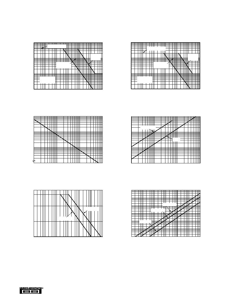
TYPICAL PERFORMANCE CURVES
T
A
= +25
°
C; V
S1
= V
S2
=
±
15V; and R
L
= 2k
, unless otherwise noted.
1
Frequency (Hz)
0
60
40
20
PSRR (dB)
PSRR vs FREQUENCY
100
10k
1M
10
1k
100k
V
S1
, V
S2
+V
S1
, +V
S2
54
100
Frequency (Hz)
10
1k
100
Peak Isolation Voltage
ISOLATION MODE VOLTAGE
vs FREQUENCY ISO121
10k
1M
100M
1k
100k
10M
5k
Max AC
Rating
Degraded
Performance
Max DC Rating
Typical
Performance
100
Frequency (Hz)
10
1k
100
Peak Isolation Voltage
ISOLATION MODE VOLTAGE
vs FREQUENCY ISO120
10k
1M
100M
1k
100k
10M
2.1k
Max AC
Rating
Degraded
Performance
Max DC Rating
Typical
Performance
1
Frequency (Hz)
0.1µA
100mA
10mA
1mA
100µA
10µA
1µA
Leakage Current (rms)
ISOLATION LEAKAGE CURRENT
vs FREQUENCY
100
10k
1M
10
1k
100k
240 Vrms
1500 Vrms
3500 Vrms
100
3dB Frequency (Hz)
0
100nF
10nF
1000pF
C
2
BANDWIDTH vs C
2
1k
10k
100k
100
Frequency (Hz)
0.1
100
10
1
Phase Shift (degrees)
PHASE SHIFT vs C
2
1k
10k
100k
C
2
= 0
C
2
= 1000pF
5
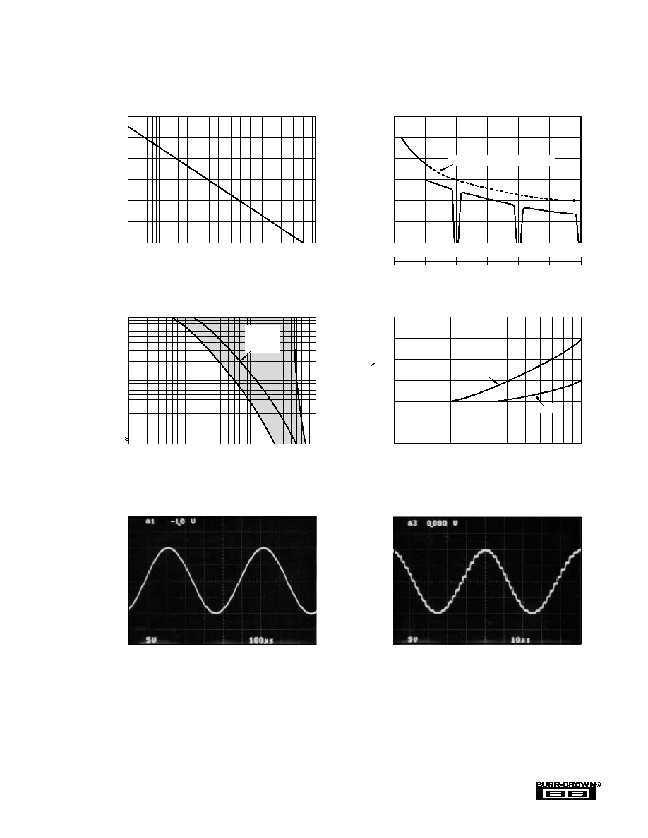
ISO120/121
TYPICAL PERFORMANCE CURVES
(CONT)
T
A
= +25
°
C; V
S1
= V
S2
=
±
15V; and R
L
= 2k
, unless otherwise noted.
1
Frequency (Hz)
40
160
140
120
100
80
60
IMR (dB)
100
10k
1M
10
1k
100k
IMR vs FREQUENCY
1k
Frequency (Hz)
0
10nF
1000pF
C
1
SYNCHRONIZATION RANGE at 25°C
±4Vp SINE WAVE INPUT TO EXT OSC
10k
100k
1M
C
2
C
1
Typical
Free Run
Frequency
0
f
IN
(Hz)
0
20
40
V
OUT
/V
IN
(dB)
SIGNAL RESPONSE vs CARRIER FREQUENCY
f
C
2f
C
3f
C
0
0
0
0
f
c
/2
f
C
/2
f
C
/2
f
OUT
(Hz)
20dB/dec (for comparison only)
0.1f
3dB
Normalized Frequency
0
12
10
8
6
4
2
Noise, e
N
(µV/ Hz)
NOISE vs SMALL SIGNAL BANDWIDTH
0.2f
3dB
0.5f
3dB
f
3dB
C
2
= 2C
1
C
2
= C
1
*
*C
1
5000pF
FPO
BLEED
TO EDGE
OF BOX
Output Voltage (V)
SINE RESPONSE
(f = 2kHz, C
2
= 0)
Time (µs)
500
0
1000
+10
0
10
Output Voltage (V)
SINE RESPONSE
(f = 20kHz, C
2
= 0)
Time (µs)
50
0
100
+10
0
10