 | –≠–ª–µ–∫—Ç—Ä–æ–Ω–Ω—ã–π –∫–æ–º–ø–æ–Ω–µ–Ω—Ç: ISO150 | –°–∫–∞—á–∞—Ç—å:  PDF PDF  ZIP ZIP |

ISO150
Dual, Isolated, Bi-Directional
DIGITAL COUPLER
q
REPLACES HIGH-PERFORMANCE
OPTOCOUPLERS
q
DATA RATE: 80M Baud, typ
q
LOW POWER CONSUMPTION:
25mW Per Channel, max
q
TWO CHANNELS, EACH BI-DIRECTIONAL,
PROGRAMMABLE BY USER
q
PARTIAL DISCHARGE TESTED: 2400Vrms
q
CREEPAGE DISTANCE OF 16.5mm (DIP)
q
LOW COST PER CHANNEL
q
PLASTIC DIP AND SOIC PACKAGES
q
DIGITAL ISOLATION FOR A/D, D/A
CONVERSION
q
ISOLATED UART INTERFACE
q
MULTIPLEXED DATA TRANSMISSION
q
ISOLATED PARALLEL TO SERIAL
INTERFACE
q
TEST EQUIPMENT
q
MICROPROCESSOR SYSTEM INTERFACE
q
ISOLATED LINE RECEIVER
q
GROUND LOOP ELIMINATION
FEATURES
APPLICATIONS
Channel 2
Channel 1
Side A
Side B
G
A
D
2A
R/T
2A
V
SA
D
1A
R/T
1A
D
2B
V
SB
R/T
2B
D
1B
G
B
R/T
1B
DESCRIPTION
The ISO150 is a two-channel, galvanically isolated
data coupler capable of data rates of 80MBaud, typi-
cal. Each channel can be individually programmed to
transmit data in either direction.
Data is transmitted across the isolation barrier by
coupling complementary pulses through high voltage
0.4pF capacitors. Receiver circuitry restores the pulses
to standard logic levels. Differential signal transmis-
sion rejects isolation-mode voltage transients up to
1.6kV/
µ
s.
ISO150 avoids the problems commonly associated
with optocouplers. Optically isolated couplers require
high current pulses and allowance must be made for
LED aging. The ISO150's Bi-CMOS circuitry oper-
ates at 25mW per channel.
ISO150 is available in a 24-pin DIP package and in a
28-lead SOIC. Both are specified for operation from
≠40∞C to 85∞C.
© 1993 Burr-Brown Corporation
PDS-1213B
Printed in U.S.A. August, 1994
International Airport Industrial Park ∑ Mailing Address: PO Box 11400 ∑ Tucson, AZ 85734 ∑ Street Address: 6730 S. Tucson Blvd. ∑ Tucson, AZ 85706
Tel: (520) 746-1111 ∑ Twx: 910-952-1111 ∑ Cable: BBRCORP ∑ Telex: 066-6491 ∑ FAX: (520) 889-1510 ∑ Immediate Product Info: (800) 548-6132

2
Æ
ISO150
The information provided herein is believed to be reliable; however, BURR-BROWN assumes no responsibility for inaccuracies or omissions. BURR-BROWN assumes
no responsibility for the use of this information, and all use of such information shall be entirely at the user's own risk. Prices and specifications are subject to change
without notice. No patent rights or licenses to any of the circuits described herein are implied or granted to any third party. BURR-BROWN does not authorize or warrant
any BURR-BROWN product for use in life support devices and/or systems.
SPECIFICATIONS
T
A
= +25
∞
C, V
S
= +5V unless otherwise noted.
ISO150AP, AU
NOTES: (1) All devices receive a 1s test. Failure criterion is
5 pulses of
5pC. (2) The voltage rate-of-change across the isolation barrier that can be sustained
without data errors. (3) Logic inputs are HCT-type and thresholds are a function of power supply voltage with approximately 0.4V hystersis--see text. (4) Supply
current measured with both tranceivers set for the indicated mode. Supply current varies with data rate--see typical curves. (5) Calculated from the maximum Pulse
Width Distortion (PWD), where Data Rate = 0.3/PWD. (6) Propagation time measured from V
IN
= 1.5V to V
O
= 2.5V. (7) The difference in propagation time of channel
A and channel B in any combination of transmission directions. (8) The difference between progagation time of a rising edge and a falling edge.
PARAMETER
CONDITION
MIN
TYP
MAX
UNITS
ISOLATION PARAMETERS
Rated Voltage, Continuous
60Hz
1500
Vrms
Partial Discharge, 100% Test
(1)
1s, 5pC
2400
Vrms
Creepage Distance (External)
DIP--"P" Package
16
mm
SOIC--"U" Package
7.2
mm
Internal Isolation Distance
0.10
mm
Isolation Voltage Transient Immunity
(2)
1.6
kV/
µ
s
Barrier Impedance
>10
14
|| 7
|| pF
Leakage Current
240Vrms, 60Hz
0.6
µ
Arms
DC PARAMETERS
Logic Output Voltage, High, V
OH
I
OH
= 6mA
V
S
≠1
V
S
V
Low, V
OL
I
OL
= 6mA
0
0.4
V
Logic Output Short-Circuit Current
Source or Sink
30
mA
Logic Input Voltage, High
(3)
2
V
S
V
Low
(3)
0
0.8
V
Logic Input Capacitance
5
pF
Logic Input Current
<1
nA
Power Supply Voltage Range
(3)
3
5
5.5
V
Power Supply Current
(4)
Transmit Mode
DC
0.001
100
µ
A
50MBaud
14
mA
Receive Mode
DC
7.2
10
mA
50MBaud
16
mA
AC PARAMETERS
Data Rate, Maximum
(5)
C
L
= 50pF
50
80
MBaud
Data Rate, Minimum
DC
Propagation Time
(6)
C
L
= 50pF
20
27
40
ns
Propagation Delay Skew
(7)
C
L
= 50pF
0.5
2
ns
Pulse Width Distortion
(8)
C
L
= 50pF
1.5
6
ns
Output Rise/Fall Time, 10% to 90%
C
L
= 50pF
9
14
ns
Mode Switching Time
Receive-to-Transmit
13
ns
Transmit-to-Receive
75
ns
TEMPERATURE RANGE
Operating Range
≠40
85
∞
C
Storage
≠40
125
∞
C
Thermal Resistance,
JA
75
∞
C/W
Æ
3
ISO150
ABSOLUTE MAXIMUM RATINGS
Storage Temperature ......................................................... ≠40
∞
C to +125
∞
C
Supply Voltages, V
S
...................................................................... ≠0.5 to 6V
Transmitter Input Voltage, V
I
............................................. ≠0.5 to V
S
+ 0.5V
Receiver Output Voltage, V
O
............................................. ≠0.5 to V
S
+ 0.5V
R/T
X
Inputs ......................................................................... ≠0.5 to V
S
+ 0.5V
Isolation Voltage dV/dt, V
ISO
............................................................ 500kV/
µ
s
D
X
Short to Ground ...................................................................... Continuous
Junction Temperature, T
J
.................................................................... 175
∞
C
Lead Temperature (soldering, 10s) ..................................................... 260
∞
C
1.6mm below seating plane (DIP package) ......................................... 300
∞
C
PACKAGE INFORMATION
(1)
PACKAGE DRAWING
MODEL
PACKAGE
NUMBER
ISO150AP
24-Pin Single-Wide DIP
243-1
ISO150AU
28-Lead SOIC
217-2
NOTE: (1) For detailed drawing and dimension table, please see end of
data sheet, or Appendix D of Burr-Brown IC Data Book.
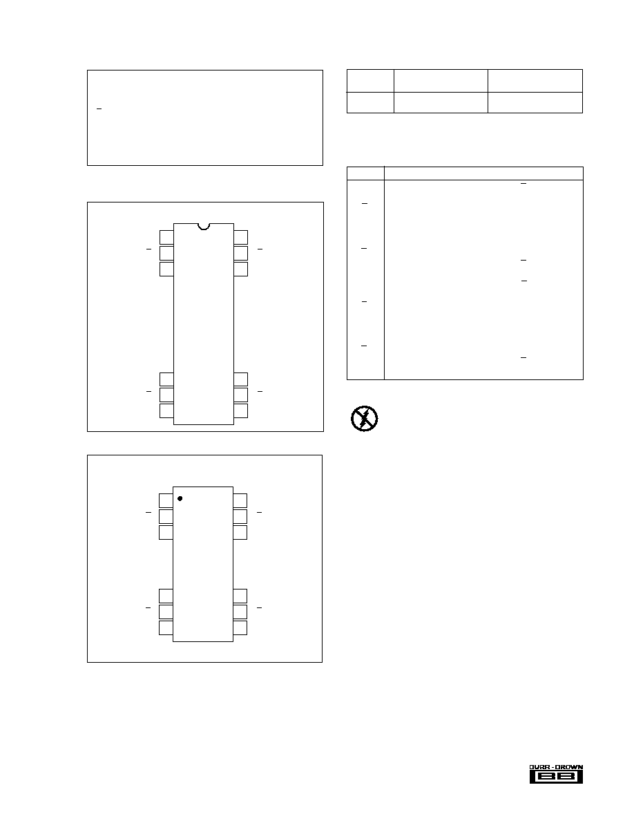
PIN CONFIGURATION
TOP VIEW
DIP
24
23
22
15
14
13
1
2
3
10
11
12
D
1A
R/T
1A
V
SA
G
B
R/T
1B
D
1B
D
2A
R/T
2A
G
A
V
SB
R/T
2B
D
2B
TOP VIEW
SOIC
PIN DESCRIPTIONS
NAME
FUNCTION
D
1A
Data in or data out for transceiver 1A. R/T
1A
held
low makes D
1A
an input pin.
R/T
1A
Receive/Transmit switch controlling transceiver 1A.
V
SA
+5V supply pin for side A which powers transceivers
1A and 2A.
G
B
Ground pin for transceivers 1B and 2B.
R/T
1B
Receive/Transmit switch controlling transceiver 1B.
D
1B
Data in or data out for transceiver 1B. R/T
1B
held
low makes D
1B
an input pin.
D
2B
Data in or data out for transceiver 2B. R/T
2B
held
low makes D
2B
an input pin.
R/T
2B
Receive/Transmit switch controlling D
2B
.
V
SB
+5V supply pin for side B which powers transceivers
1B and 2B.
G
A
Ground pin for transceivers 1A and 2A.
R/T
2A
Receive/Transmit switch controlling transceiver 2A.
D
2A
Data in or data out for transceiver 2A. R/T
2A
held
low makes D
2A
in input pin.
ELECTROSTATIC
DISCHARGE SENSITIVITY
This integrated circuit can be damaged by ESD. Burr-Brown
recommends that all integrated circuits be handled with ap-
propriate precautions. Failure to observe proper handling and
installation procedures can cause damage.
ESD damage can range from subtle performance degradation
to complete device failure. Precision integrated circuits may
be more susceptible to damage because very small parametric
changes could cause the device not to meet its published
specifications.
28
27
26
17
16
15
1
2
3
12
13
14
D
1A
R/T
1A
V
SA
G
B
R/T
1B
D
1B
D
2A
R/T
2A
G
A
V
SB
R/T
2B
D
2B
4
Æ
ISO150
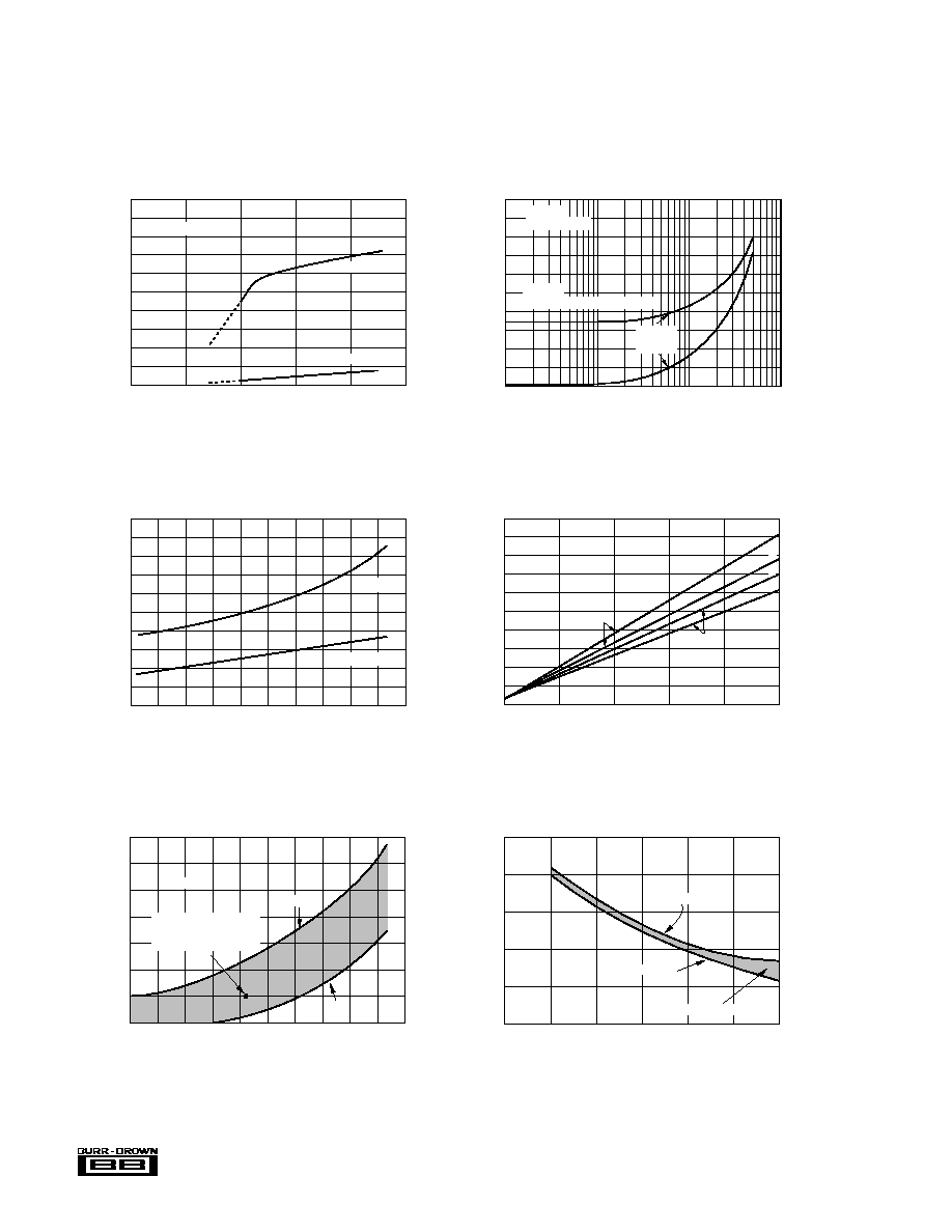
TYPICAL PERFORMANCE CURVES
T
A
= +25
∞
C, V
S
= +5V unless otherwise noted.
SUPPLY CURRENT PER CHANNEL
vs TEMPERATURE
Temperature (∞C)
≠60
6
5
4
3
2
1
≠40
≠20
0
20
40
60
80
100
120
140
Supply Current (mA)
V
S
= 5.0V
V
S
= 3.0V
NORMALIZED RISE/FALL TIME vs TEMPERATURE
1.6
1.5
1.4
1.3
1.2
1.1
1.0
.9
≠60
≠40
≠20
0
20
40
60
80
100
120
140
Temperature (∞C)
Relative t
r
, t
f
C
L
= 50pF
Normalized to Average
of Many Devices
at 25∞C
+1
≠1
SUPPLY CURRENT PER CHANNEL
vs SUPPLY VOLTAGE
5
4
3
2
1
1
2
3
4
5
6
Supply Voltage, V
S
(V)
Supply Current (mA)
C
L
= 15pF
Receive Mode
Transmit Mode
0
f = 1MHz = 2MBaud
POWER CONSUMPTION PER CHANNEL vs FREQUENCY
Frequency (Hz)
100k
1M
10M
100M
Power (mW)
Supply Current (mA)
50
40
30
20
10
0
10
8
6
4
2
0
Receive
Transmit
No Load
One Channel
NOTE:
Baud Rate = 2 ∑ Frequency
TYPICAL RISE AND FALL TIMES vs CAPACITIVE LOAD
vs SUPPLY VOLTAGE
100
80
60
40
20
0
0
100
200
300
400
500
Capacitive Load (pF)
t
r
, t
f
(ns)
V
S
= 3.0V
V
S
= 5.0V
t
r
t
f
t
f
t
r
PROPAGATION DELAY vs SUPPLY VOLTAGE
45
40
35
30
25
20
2.5
3.0
3.5
4.0
4.5
5.0
5.5
Supply Voltage, V
S
(V)
Propagation Delay (ns)
Low to High
High to Low
Pulse Width Distortion

Æ
5
ISO150
TYPICAL PERFORMANCE CURVES
(CONT)
T
A
= +25
∞
C, V
S
= +5V unless otherwise noted.
ISOLATION VOLTAGE vs FREQUENCY
10k
2.1k
1k
100
10
1
1k
10k
100k
1M
10M
100M
Frequency (Hz)
Peak Isolation Voltage (V)
Max DC
Rating
Degraded
Performance
PULSE WIDTH DISTORTION
vs TEMPERATURE
Temperature (∞C)
≠60
5
4
3
2
1
0
≠40
≠20
0
20
40
60
80
100
120
140
Pulse Width Distortion, PWD (ns)
V
S
= 5.0V
C
L
= 50pF
OUTPUT VOLTAGE vs LOGIC INPUT VOLTAGE
5
4
3
2
1
0
0.5
1.0
1.5
2.0
V
IN
(V)
V
OUT
(V)
PROPAGATION DELAY vs TEMPERATURE
60
50
40
30
20
10
0
≠60
≠40
≠20
0
20
40
60
80
100 120
140
Temperature (∞C)
Propagation Delay, t
PD
(ns)
V
S
= 3.0V
V
S
= 5.0V
C
L
= 50pF
LOGIC INPUT THRESHOLD VOLTAGE
vs SUPPLY VOLTAGE
2.0
1.8
1.6
1.4
1.2
1.0
0.8
0.6
0.4
0.2
0
2.0
2.5
3.0
3.5
4.0
4.5
5.0
5.5
6.0
Supply Voltage, V
SS
(V)
V
IN
(V)
V
T LOW
, ≠40∞C
V
T HIGH
, 125∞C
ISOLATION LEAKAGE CURRENT vs FREQUENCY
100m
10m
1m
100µ
10µ
1µ
100n
1
10
100
1k
10k
100k
1M
Frequency (Hz)
Leakage Current (Arms)
V
ISO
= 240Vrms
V
ISO
= 1500Vrms