 | –≠–ª–µ–∫—Ç—Ä–æ–Ω–Ω—ã–π –∫–æ–º–ø–æ–Ω–µ–Ω—Ç: CM1414 | –°–∫–∞—á–∞—Ç—å:  PDF PDF  ZIP ZIP |

©
2005 California Micro Devices Corp. All rights reserved.
11/03/05
490 N. McCarthy Blvd., Milpitas, CA 95035-5112
Tel: 408.263.3214
Fax: 408.263.7846
www.calmicro.com
1
CM1414
2 Channel Headset EMI Filter with ESD Protection
Features
∑
Functionally and pin compatible with CMD's
CSPEMI204
∑
OptiGuard
TM
coated for improved reliability at
assembly
∑
Two channels of EMI filtering, one for a micro-
phone and one for an earpiece speaker
∑
Pi-style EMI filters in a capacitor-resistor-capacitor
(C-R-C) network
∑
Greater than 35dB attenuation in the 800-
2700MHz range
∑
+
8kV ESD protection on each channel (IEC 61000-
4-2 Level 4, contact discharge)
∑
+
15kV ESD protection on each channel (HBM)
∑
Chip Scale Package features extremely low para-
sitic inductance for optimum filter performance
∑
5-bump, 0.950mm X 1.41mm footprint
Chip Scale Package (CSP)
∑
Lead-free version available
Applications
∑
EMI filtering and ESD protection for headset micro-
phone and earpiece speaker ports
∑
Cellular / Mobile Phones
∑
Notebooks and Personal Computers
∑
Handheld PCs / PDAs / Tablets
∑
Wireless Handsets
∑
Digital Camcorders
Product Description
The CM1414 is a low-pass filter array designed specifi-
cally to reduce EMI/RFI emissions and provide ESD
protection for a headset port on a cellular and mobile
devices. The CM1414 integrates two high quality, pi-
style filters (C-R-C) filters, one for a microphone and
one for an earpiece or speaker, each providing more
than 35dB attenuation relative to the pass band attenu-
ation in the 800-2700 MHz range. These filters support
bidirectional filtering, reducing EMI both to and from
the headset port and support bipolar audio signals
without distortion.
In addition, the CM1414 provides a very high level of
protection for sensitive electronic components that may
be subject to electrostatic discharge (ESD). The input
pins are designed and characterized to safely dissipate
ESD strikes of
+
8kV contact discharge, the maximum
requirement of the IEC 61000-4-2 international stan-
dard. Using the MIL-STD-883 (Method 3015) specifica-
tion for Human Body Model (HBM) ESD, the device
provides protection for contact discharges to greater
than
+
15kV. The CM1414 protects sensitive compo-
nents such as CPU and DSPs that have much weaker
internal ESD protection circuitry usually only intended
for mechanical handling protection.
The CM1414 is particularly well suited for portable
electronics because of its small package format and
low weight. The CM1414 incorporates OptiGuard
TM
coating which results in improved reliability at assem-
bly and is available in a space-saving, low-profile Chip
Scale Package with optional lead-free finishing.
Electrical Schematic
10
100pF
100pF
EAR_IN
C1
B2
GND
A1
EAR_OUT
68
47pF
47pF
MIC_IN
C3
A3
MIC_OUT
©
2005 California Micro Devices Corp. All rights reserved.
2
490 N. McCarthy Blvd., Milpitas, CA 95035-5112
Tel: 408.263.3214
Fax: 408.263.7846
www.calmicro.com
11/03/05
CM1414
Ordering Information
Note 1: Parts are shipped in Tape & Reel form unless otherwise specified.
Note 2: Lead-free devices are specified by using a "
+
" character for the top side orientation mark.
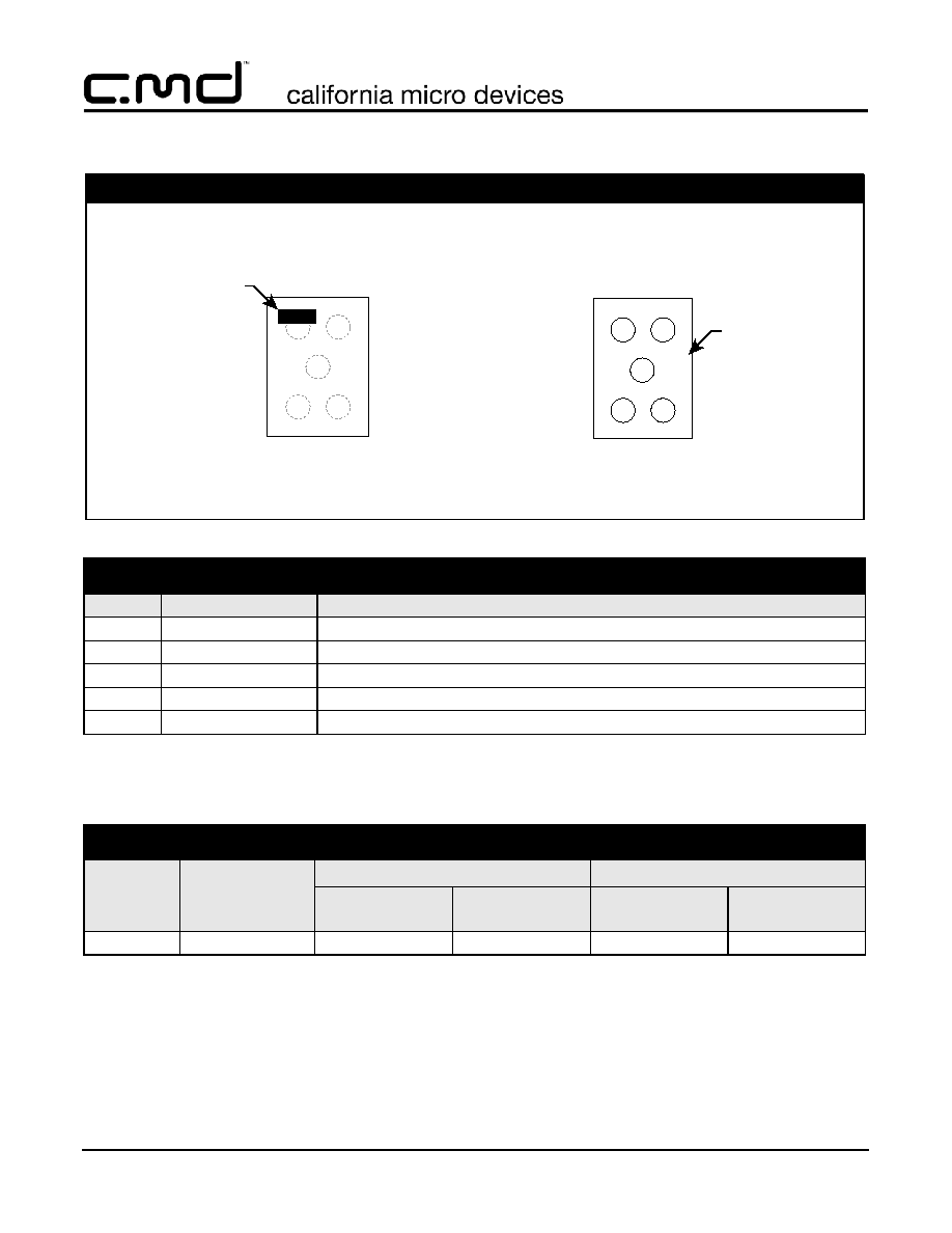
PIN DESCRIPTIONS
PIN
NAME
DESCRIPTION
A1
EAR_IN
Earpiece Input (from audio circuitry)
A3
MIC_IN
Microphone Input (from microphone)
B2
GND
Device Ground
C1
EAR_OUT
Earpiece Output (to earpiece)
C3
MIC_OUT
Microphone Output (to audio circuitry)
CC
3
1 2
C
B
A
Orientation
Marking
(see note 2)
CM1414
CSP Package
MIC_OUT
EAR_OUT
GND
MIC_IN
EAR_IN
C3
Orientation
Marking
C1
B2
A1
A3
A1
PACKAGE / PINOUT DIAGRAMS
Notes:
TOP VIEW
BOTTOM VIEW
(Bumps Down View)
(Bumps Up View)
1) These drawings are not to scale.
2)
Lead-free devices are specified by using a "+" character for the top side orientation mark.
PART NUMBERING INFORMATION
Bumps
Package
Standard Finish
Lead-free Finish
2
Ordering Part
Number
1
Part Marking
Ordering Part
Number
1
Part Marking
5
CSP
CM1414-03CS
CC
CM1414-03CP
CC

©
2005 California Micro Devices Corp. All rights reserved.
11/03/05
490 N. McCarthy Blvd., Milpitas, CA 95035-5112
Tel: 408.263.3214
Fax: 408.263.7846
www.calmicro.com
3
CM1414
Specifications
Note 1: T
A
=25
∞
C unless otherwise specified.
Note 2: ESD applied to input and output pins with respect to GND, one at a time.
Note 3: Clamping voltage is measured at the opposite side of the EMI filter to the ESD pin. For example, if ESD is applied to Pin A1,
then clamping voltage is measured at Pin C1.
Note 4: Unused pins are left open
Note 5: The parameters are guaranteed by design.
Note 6: Z
SOURCE
=50
, Z
LOAD
=50
ABSOLUTE MAXIMUM RATINGS
PARAMETER
RATING
UNITS
Storage Temperature Range
-65 to +150
∞C
DC Power per Resistor
100
mW
DC Package Power Rating
300
mW
STANDARD OPERATING CONDITIONS
PARAMETER
RATING
UNITS
Operating Temperature Range
-40 to +85
∞C
ELECTRICAL OPERATING CHARACTERISTICS
(NOTE 1)
SYMBOL
PARAMETER
CONDITIONS
MIN
TYP
MAX
UNITS
R
1
Resistance
9
10
11
R
2
Resistance
54
68
75
C
1
Capacitance
80
100
120
pF
C
2
Capacitance
38
47
57
pF
I
LEAK
Diode Leakage Current
V
IN
=5.0V
1.0
A
V
SIG
Signal Voltage
Positive Clamp
Negative Clamp
I
LOAD
= 10mA
5
-15
7
-10
15
-5
V
V
V
ESD
In-system ESD Withstand Voltage
a) Human Body Model, MIL-STD-883,
Method 3015
b) Contact Discharge per IEC 61000-4-2
Level 4
Notes 2,4 and 5
±15
±8
kV
kV
V
CL
Clamping Voltage during ESD Discharge
MIL-STD-883 (Method 3015), 8kV
Positive Transients
Negative Transients
Notes 2,3,4 and 5
+15
-19
V
V
f
C1
Cut-off frequency 1; Note 6
R = 10
, C = 100pF
33
MHz
f
C2
Cut-off frequency 2; Note 6
R = 68
, C = 47pF
61
MHz

©
2005 California Micro Devices Corp. All rights reserved.
4
490 N. McCarthy Blvd., Milpitas, CA 95035-5112
Tel: 408.263.3214
Fax: 408.263.7846
www.calmicro.com
11/03/05
CM1414
Performance Information
Typical Filter Performance (nominal conditions unless specified otherwise, 50 Ohm Environment)
Figure 1. Earpiece Circuit (A1-C1) EMI Filter Performance
Figure 2. Microphone Circuit (A3-C3) EMI Filter Performance
©
2005 California Micro Devices Corp. All rights reserved.
11/03/05
490 N. McCarthy Blvd., Milpitas, CA 95035-5112
Tel: 408.263.3214
Fax: 408.263.7846
www.calmicro.com
5
CM1414
Application Information
Refer to Application Note AP-217, "The Chip Scale Package", for a detailed description of Chip Scale Packages
offered by California Micro Devices.
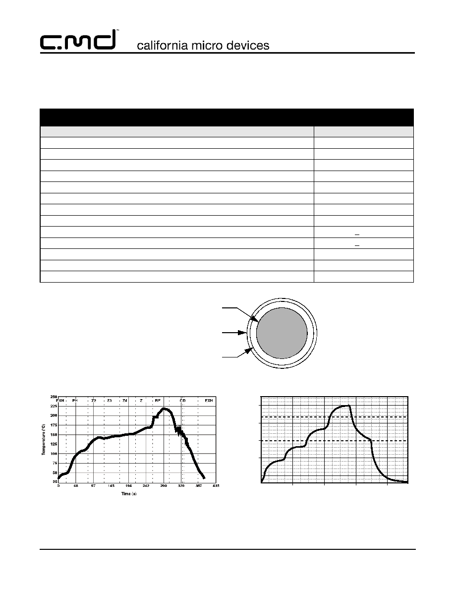
Figure 3. Recommended Non-Solder Mask Defined Pad Illustration
Figure 4. Eutectic (SnPb) Solder
Ball Reflow Profile
Figure 5. Lead-free (SnAgCu) Solder
Ball Reflow Profile
PRINTED CIRCUIT BOARD RECOMMENDATIONS
PARAMETER
VALUE
Pad Size on PCB
0.275mm Round
Pad Definition
Non-Solder Mask defined pads
Solder Mask Opening
0.325mm Round
Solder Stencil Thickness
0.125 - 0.150mm
Solder Stencil Aperture Opening (laser cut, 5% tapered walls)
0.330mm Round
Solder Flux Ratio
50/50 by volume
Solder Paste Type
No Clean
Pad Protective Finish
OSP (Entek Cu Plus 106A)
Tolerance -- Edge To Corner Ball
+50
m
Solder Ball Side Coplanarity
+20
m
Maximum Dwell Time Above Liquidous
60 seconds
Maximum Soldering Temperature for Eutectic Devices using a Eutectic Solder Paste
240∞C
Maximum Soldering Temperature for Lead-free Devices using a Lead-free Solder Paste
260∞C
Solder Mask Opening
0.325mm DIA.
Non-Solder Mask Defined Pad
0.275mm DIA.
Solder Stencil Opening
0.330mm DIA.
200
250
150
100
50
0
1:00.0
2:00.0
3:00.0
4:00.0
Time (minutes)
T
emperature
(∞
C)

©
2005 California Micro Devices Corp. All rights reserved.
6
490 N. McCarthy Blvd., Milpitas, CA 95035-5112
Tel: 408.263.3214
Fax: 408.263.7846
www.calmicro.com
11/03/05
CM1414
Mechanical Details
CSP Mechanical Specifications
CM1414 devices are packaged in a custom Chip Scale
Package (CSP). Dimensions are presented below. For
complete information on CSP packaging, see the Cali-
fornia Micro Devices CSP Package Information docu-
ment.
Package Dimensions for CM1414
Chip Scale Package
CSP Tape and Reel Specifications
Figure 6. Tape and Reel Mechanical Data
PACKAGE DIMENSIONS
Package
Custom CSP
Bumps
5
Dim
Millimeters
Inches
Min
Nom
Max
Min
Nom
Max
A1
0.905 0.950 0.995 0.0356 0.0374 0.0392
A2
1.365 1.410 1.455 0.0537 0.0555 0.0573
B1
0.495 0.500 0.505 0.0195 0.0197 0.0199
B2
0.245 0.250 0.255 0.0096 0.0098 0.0100
B3
0.430 0.435 0.440 0.0169 0.0171 0.0173
B4
0.430 0.435 0.440 0.0169 0.0171 0.0173
C1
0.175 0.225 0.275 0.0069 0.0089 0.0108
C2
0.220 0.270 0.320 0.0087 0.0106 0.0126
D1
0.575 0.644 0.714 0.0226 0.0254 0.0281
D2
0.368 0.419 0.470 0.0145 0.0165 0.0185
# per tape and
reel
3500 pieces
Controlling dimension: millimeters
Mechanical Package Diagrams
A
B
C
1 2
C1
B1
A1
B3
C2
DIMENSIONS IN MILLIMETERS
D1
D2
A2
BOTTOM VIEW
SIDE
VIEW
3
B2
B4
0.30 DIA.
63/37 Sn/Pb (Eutectic) or
SOLDER BUMPS
96.8/2.6/0.6 Sn/Ag/Cu (Lead-free)
OptiGuard
TM
Coating
PART NUMBER
CHIP SIZE (mm)
POCKET SIZE (mm)
B
0
X A
0
X K
0
TAPE WIDTH
W
REEL
DIAMETER
QTY PER
REEL
P
0
P
1
CM1414
1.41 X 0.95 X 0.644
1.52 X 1.07 X 0.720
8mm
178mm (7")
3500
4mm
4mm
Top
For tape feeder reference
Cover
Tape
P
1
only including draft.
Concentric around B.
K
o
Embossment
User direction of feed
±
0.2 mm
P
o
Center lines
of cavity
W
10 Pitches cumulative
tolerance on tape
A
o
B
o