 | ÐлекÑÑоннÑй компоненÑ: CSPEMI607 | СкаÑаÑÑ:  PDF PDF  ZIP ZIP |
Äîêóìåíòàöèÿ è îïèñàíèÿ www.docs.chipfind.ru
California Micro Devices
430 N.McCarthy Blvd
Milpitas, CA 95035
PRELIMINARY
11/18/03 Tel: (408) 263-3214
·
Fax: (408) 263-7846
·
Website:
www.calmicro.com
1
CSPEMI607
4-Channel LCD EMI Filter Array with ESD Protection plus
4-Channel of ESD Protection Array
Features
Applications
·
Four channels of EMI filtering
·
Four channels of ESD Protection
·
±
15kV ESD protection
(IEC 61000-4-2, contact discharge)
·
±
30kV ESD protection (HBM)
·
Better than 30dB of attenuation at 1GHz for 15pF-
100
-15pF filter configuration
·
Chip scale packaging features extremely low lead
inductance for optimum filter and ESD
performance
·
LCD data lines in mobile handsets
·
I/O port protection for mobile handsets, notebook
computers, PDAs etc.
·
EMI filtering for data ports in cell phones, PDAs or
notebook computers.
General Description
CAMD's CSPEMI607 is an EMI filter array with ESD protection, which integrates four Pi- filters (C-R-
C) and 4 channels of ESD protection. The CSPEMI607 has component values of 15pF-100
-15pF
). The parts include avalanche-type ESD diodes on every pin, which provide a very high level of
protection for sensitive electronic components that may be subjected to electrostatic discharge
(ESD). The ESD diodes connected to the filter ports and the standalone ESD diode channels are
designed and characterized to safely dissipate ESD strikes of
±
15kV, beyond the maximum
requirement of the IEC 61000-4-2 international standard. Using the MIL-STD-883 (Method 3015)
specification for Human Body Model (HBM) ESD, the pins are protected for contact discharges at
greater than
±
30kV.
This device is particularly well suited for portable electronics (e.g. mobile handsets, PDAs, notebook
computers) because of its small package format and easy-to-use pin assignments. In particular, the
CSPEMI607 is ideal for EMI filtering and protecting data lines from ESD for the LCD display in
mobile handsets.
The CSPEMI607 is available in a space-saving, low-profile, chip-scale package, and is fabricated
with one of California Micro Devices' semiconductor processes.
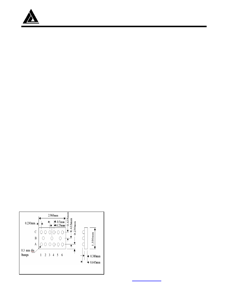
Package Diagram
California Micro Devices
430 N.McCarthy Blvd
Milpitas, CA 95035
PRELIMINARY
11/18/03 Tel: (408) 263-3214
·
Fax: (408) 263-7846
·
Website:
www.calmicro.com
2
Figure 1. Dimensions of CSPEMI607.
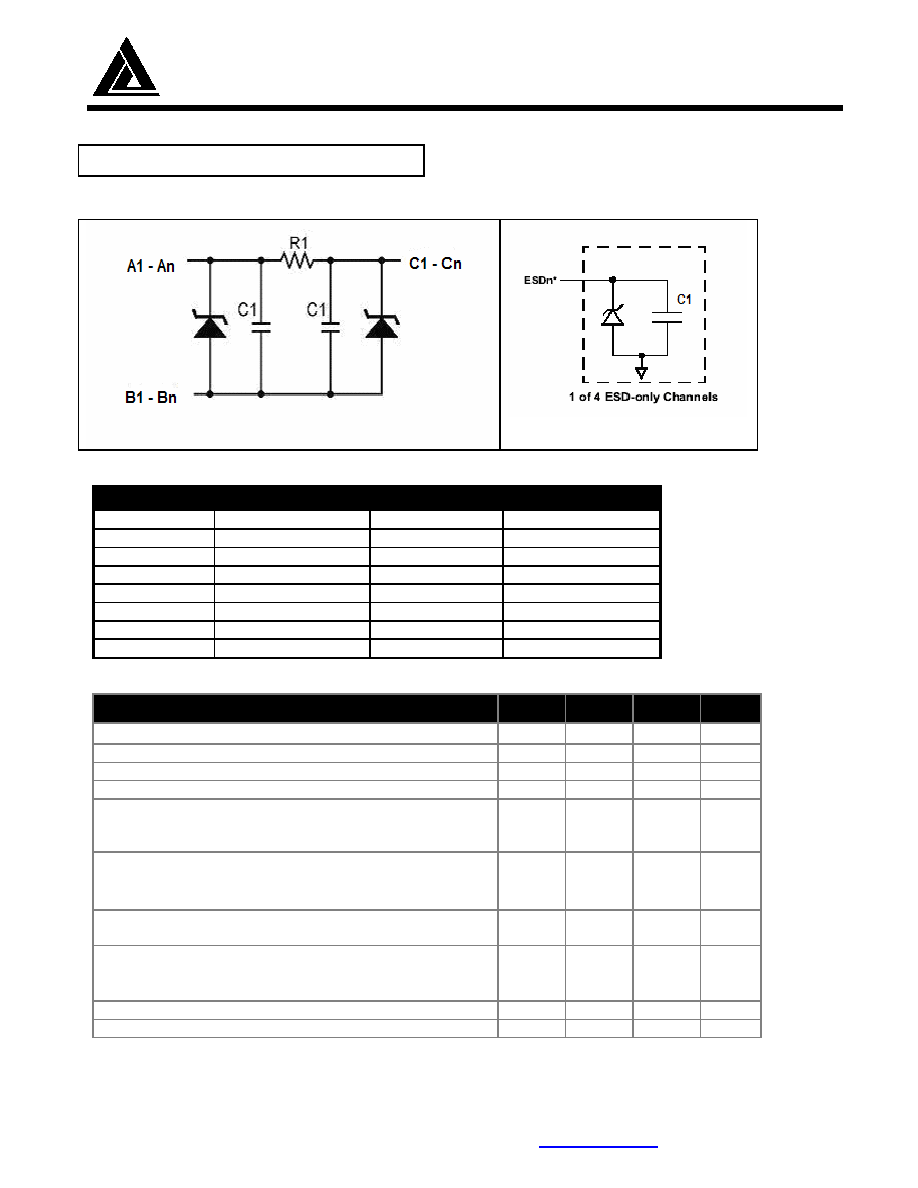
Schematic Diagram
Pin Number Pin Description
Pin Number
Pin Description
A1
ESD Channel #1
B3
GND
A2
Filter #1
C1
ESD Channel #3
A3
Filter #2
C2
Filter #1
A4
Filter #3
C3
Filter #2
A5
Filter #4
C4
Filter #3
A6
ESD Channel #2
C5
Filter #4
B1
GND
C6
ESD Channel #4
B2
GND
Specifications:
(At 25
°
C unless specified otherwise)
Min.
Typ.
Max. Unit
Resistance R1
80
100
120
Capacitance C1 at 2.5V dc; 1MHz, 30mV ac
12
15
18
pF
Stand-off Voltage, I = 10µA
5.5
V
Diode Leakage at +/-3.3V reverse bias voltage
100
nA
Signal Clamp Voltage:
Positive Clamp, 10mA
Negative Clamp, -10mA
5.6
-1.5
6.8
-0.8
9.0
-0.4
V
V
In-system ESD withstand voltage*:
Human Body Model (MIL-STD-883, method 3015)
IEC 61000-4-2, contact discharge method
±
30
±
15
kV
kV
Clamping voltage during ESD discharge* Positive
MIL-STD-883 (Method 3015), 8kV Negative
12
-7
V
V
Temperature Range:
Operating
Storage
-40
-65
85
150
°
C
DC Power per Resistor:
0.1
W
DC Package Power Rating:
0.5
W
* ESD applied to input / output pins with respect to GND, one at a time. Clamping voltage is
measured at the opposite side of the EMI filter to the ESD pin (i.e. if ESD is applied to pin A1
then clamping voltage is measured at pin C1). Unused pins are left open. These parameters
are guaranteed by design.
California Micro Devices
430 N.McCarthy Blvd
Milpitas, CA 95035
PRELIMINARY
11/18/03 Tel: (408) 263-3214
·
Fax: (408) 263-7846
·
Website:
www.calmicro.com
3
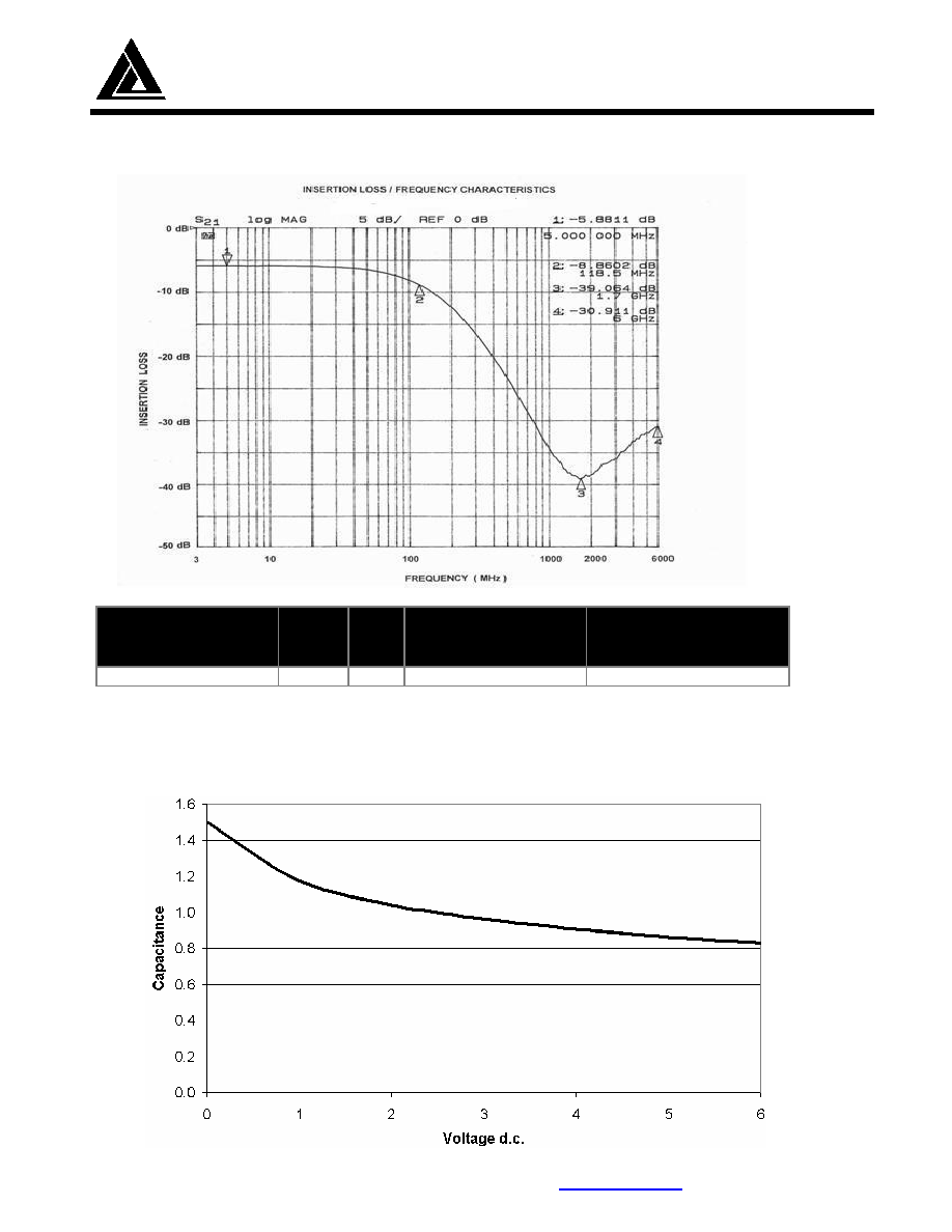
Typical EMI filter performance
(2.5V d.c., 50
environment)
Cut-off Frequency
(MHz)
R1
(
)
C1
(pF)
20dB Attenuation
(MHz)
Over 25dB Range
(MHz)
118
100
15
533
738 - 3000
All parameters in the table are typical values.
Typical diode capacitance vs. input voltage
(normalized to 2.5V d.c.)
California Micro Devices
430 N.McCarthy Blvd
Milpitas, CA 95035
PRELIMINARY
11/18/03 Tel: (408) 263-3214
·
Fax: (408) 263-7846
·
Website:
www.calmicro.com
4
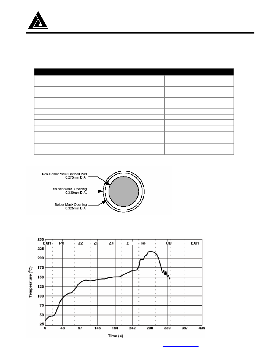
PRINTED CIRCUIT BOARD RECOMMENDATIONS
Pad size in PCB
0.275mm
Pad Shape
Round
Pad Definition
Non Solder Mask Defined Pads
Solder Mask Opening
0.325mm Round
Solder Stencil Thickness
0.125mm - 0.150mm
Solder Stencil Aperture Opening (Laser cut, 5% tapered walls)
0.330mm (round)
Solder Flux Ratio
50/50 by volume
Solder Paste Type
No Clean
Bond Trace Finish
OSP (Entek Cu Plus 106A)
Tolerance Edge to Corner Ball
±
50µm
Solder Ball Side Coplanarity
±
20µm
Soldering Minimum Temperature
205'C for at least 30 seconds
Maximum Dwell Time above Liquidous (183°C)
60 seconds
Soldering Maximum Temperature
240'C for at less than 2 minutes
Solder Reflow Profile
California Micro Devices
430 N.McCarthy Blvd
Milpitas, CA 95035
PRELIMINARY
11/18/03 Tel: (408) 263-3214
·
Fax: (408) 263-7846
·
Website:
www.calmicro.com
5
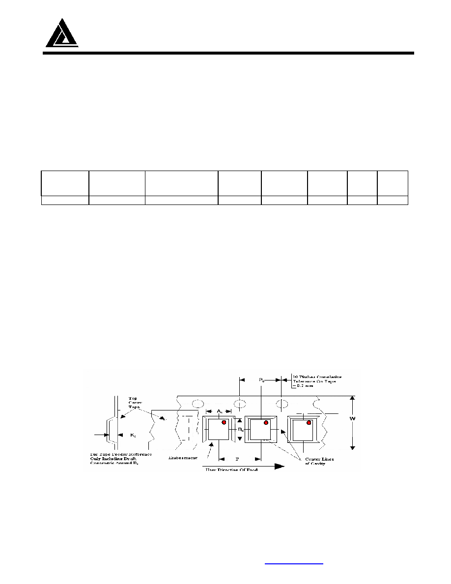
Tape & Reel Information
CMD PART # CHIP SIZE
(mm)
POCKET SIZE
(mm)
Bo x Ao x Ko
TAPE
WIDTH
W
REEL
DIAMETER
QTY PER
REEL
P
0
P
1
CSPEMI607
2.96 x 1.33 x 0.6
TBD
8mm
178mm (7")
3500
4mm
4mm