
PS7801C-1A
NEC's
4-PIN ULTRA SMALL FLAT-LEAD
SUPER LOW OUTPUT CAPACITANCE
1-ch OPTICAL COUPLED MOS FET
California Eastern Laboratories
∑
ULTRA SMALL FLAT-LEAD PACKAGE:
4.2 (L) ◊ 2.5 (W) ◊ 1.85 (H) mm
∑ SUPER LOW OUTPUT CAPACITANCE:
C
out
= 0.5 pF TYP.
∑
LOW C ◊ R:
C ◊ R = 6.5 pF ∑
∑
1 CHANNEL TYPE:
1 a output
∑
DESIGN FOR AC/DC SWITCHING LINE CHANGER
∑
LOW OFFSET VOLTAGE
∑
ORDERING NUMBER OF TAPING PRODUCT:
PS7801C-1A-F3, F4: 3 500 pcs/reel
FEATURES
PRELIMINARY DATA SHEET
NEC's PS7801C-1A is a low output capacitance solid
state relay containing a GaAs LED on the light emit-
ting side (input side) and MOS FETs on the output
side.
An ultra small flat-lead package has been provided
which realizes a reduction in mounting area of about
50% compared with the PS72xx series.
It is suitable for high-frequency signal control, due to
its low C ◊ R, super low output capacitance, and low
off-state leakage current.
DESCRIPTION
∑
Measurement Equipment
APPLICATION

PS7801C-1A
PACKAGE DIMENSIONS (UNIT: mm)
MARKING EXAMPLE
3.6
+0.
3
-0.4
2.5±0.3
4
3
1
2
N
4.2±0.2
0.2 MAX.
0.2±0.1
3.0 MAX.
1.27
1.85±0.05
0.4±0.1
1. LED Anode
2. LED Cathode
3. MOS FET
4. MOS FET
4
3
1
2
TOP VIEW
0.15
+0.
1
-0.0
5
0.2±0.1
0.36
4.6±0.2
503
5
N
03
Assembly lot
Week assembled
Year assembled
No.1 pin
mark
(knicked
corner)
An initial of "NEC"
(Marking details)
Last number of
type No. : 1C
*1
*2
*1 The marking corresponds to the last two digits
of the part number below.
PS7801C-1A
*2 Bar : Pb-Free
1C

PS7801C-1A
ORDERING INFORMATION
ABSOLUTE MAXIMUM RATINGS
(T
A
= 25∫C, unless otherwise Specified)
PART NUMBER
ORDER NUMBER
SOLDER PLATING
SPECIFICATION
PACKING STYLE
PS7801C-1A-F3
PS7801C-1A-F3-A
Pb-Free
Embossed Tape 3 500 pcs/reel
PS7801C-1A-F4
PS7801C-1A-F4-A
PARAMETER
SYMBOL
RATINGS
UNIT
Diode
Forward Current (DC)
I
F
50
mA
Reverse Voltage
V
R
5.0
V
Power Dissipation
P
D
50
mW
Peak Forward Current
*1
I
FP
1
A
MOS FET Break Down Voltage
V
L
30
V
Continuous Load Current
I
L
80
mA
Pulse Load Current
*2
(AC/DC Connection)
I
LP
160
mA
Power Dissipation
P
D
250
mW
Isolation Voltage
*3
BV
500
Vr.m.s.
Total Power Dissipation
P
T
300
mW
Operating Ambient Temperature
T
A
-
40 to +85
∞
C
Storage Temperature
T
stg
-
40 to +100
∞
C
*1 PW = 100 s, Duty Cycle = 1%
*2 PW = 100 ms, 1 shot
*3 AC voltage for 1 minute at T
A
= 25∞C, RH = 60% between input and output.
Pins 1-2 shorted together, 3-4 shorted together.
RECOMMENDED OPERATING CONDITIONS
(T
A
= 25∫C)
PARAMETER
SYMBOL
MIN.
TYP.
MAX.
UNIT
LED Operating Current
I
F
2
5
20
mA
LED Off Voltage
V
F
0
0.5
V
PS7801C-1A
ELECTRICAL CHARACTERISTICS
(T
A
= 25 85∫C)
PARAMETER
SYMBOL
CONDITIONS
MIN.
TYP.
MAX.
UNIT
Diode
Forward Voltage
V
F
I
F
= 5 mA
1.1
1.4
V
Reverse Current
I
R
V
R
= 5 V
5.0
A
MOS FET
Off-state Leakage Current
I
Loff
V
D
= 30 V
0.1
1.0
nA
Output Capacitance
C
out
V
D
= 0 V, f = 1 MHz
0.5
0.7
pF
Coupled
LED On-state Current
I
Fon
I
L
= 80 mA
2.0
mA
On-state Resistance
R
on
I
F
= 5 mA, I
L
= 80 mA
13
17
Turn-on Time
*1, 2
t
on
I
F
= 5 mA, V
O
= 5 V, R
L
= 500 ,
PW 10 ms
0.03
0.5
ms
Turn-off Time
*1, 2
t
off
0.1
0.5
Isolation Resistance
R
I-O
V
I-O
= 0.5 kV
DC
10
9
Isolation Capacitance
C
I-O
V = 0 V, f = 1 MHz
0.3
pF
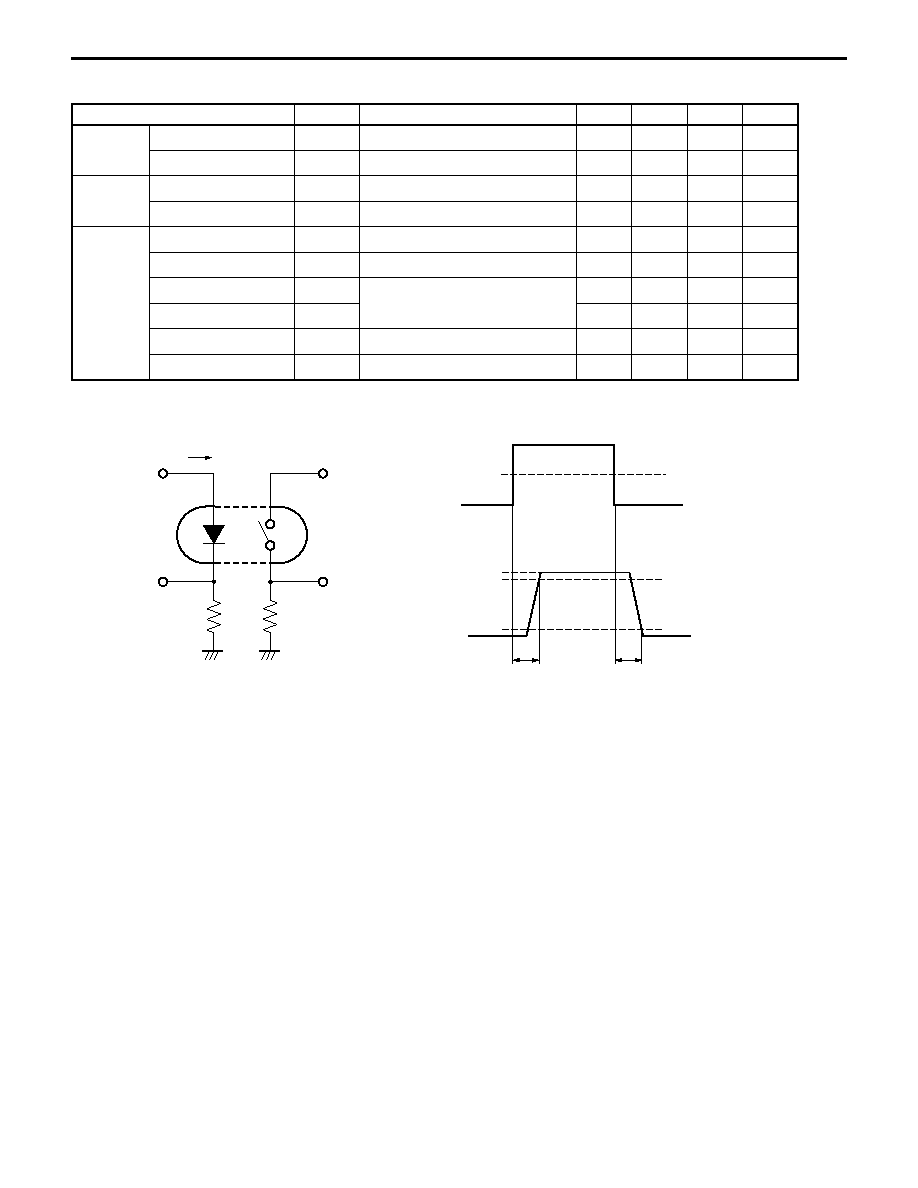
*1 Test Circuit for Switching Time
*2 The turn-on time and turn-off time are specified as input-pulse width 10 ms.
Be aware that when the device operates with an input-pulse width less than 10 ms, the turn-on time and turn-off time
will increase.
Pulse Input
Input monitor
monitor
V
O
V
L
R
L
I
F
R
in
t
on
t
off
10%
90%
Input
0
Output
V
O
= 5 V
50%
PS7801C-1A
Life Support Applications
These NEC products are not intended for use in life support devices, appliances, or systems where the malfunction of these products can reasonably
be expected to result in personal injury. The customers of CEL using or selling these products for use in such applications do so at their own risk and
agree to fully indemnify CEL for all damages resulting from such improper use or sale.
A Business Partner of NEC Compound Semiconductor Devices, Ltd.
04/11/2005
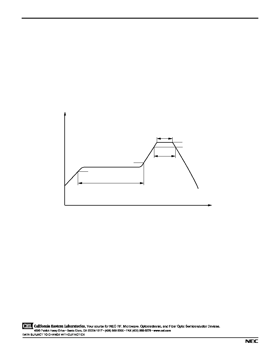
NOTES ON HANDLING
Recommended soldering conditions
(1) Infrared reflow soldering
∑ Peak reflow temperature
260∞C or below (package surface temperature)
∑ Time of peak reflow temperature
10 seconds or less
∑ Time of temperature higher than 220∞C
60 seconds or less
∑ Time to preheat temperature from 120 to 180∞C 120±30 s
∑ Number of reflows
Three
∑ Flux
Rosin flux containing small amount of chlorine (The flux with a
maximum chlorine content of 0.2 Wt% is recommended.)
(2) Wave soldering
∑ Temperature
260∞C or below (molten solder temperature)
∑ Time
10 seconds or less
∑ Preheating conditions 120∞C or below (package surface temperature)
∑ Number of times
One
∑ Flux
Rosin flux containing small amount of chlorine (The flux with a maximum chlorine content of 0.2
Wt% is recommended.)
(3) Cautions
∑ Fluxes
Avoid removing the residual flux with freon-based and chlorine-based cleaning solvent.
220∫C
Package Surface T
emperature T
(∫C)
Time (s)
(heating)
to 10 s
to 60 s
260∫C MAX.
Recommended Temperature Profile of Infrared Reflow
120±30 s
(preheating)
180∫C
120∫C