SILICON RFIC
LOW CURRENT AMPLIFIER
FOR MOBILE COMMUNICATIONS
UPC8178TB
DESCRIPTION
NEC'S UPC8178TB is a silicon monolithic integrated circuit
designed as an amplifier for mobile communications. This IC
can realize low current consumption with an external chip
inductor which cannot be realized on an internal 50 wideband
matched IC. This low current amplifier operates on 3.0 V. This
device is manufactured using NEC's 30 GHz fmax UHS0 (Ultra
High Speed Process) silicon bipolar process which uses direct
silicon nitride passivation film and gold electrodes. These
materials can protect the chip surface from pollution and
prevent corrosion/migration. Thus, this IC has excellent perfor-
mance, uniformity and reliability.
NEC's stringent quality assurance and test procedures ensure
the highest reliability and performance.
California Eastern Laboratories
APPLICATIONS
∑
Buffer Amplifiers on 0.1 to 2.4 GHz mobile
communications system
PART NUMBER
UPC8178TB
PACKAGE OUTLINE
S06
SYMBOLS
PARAMETERS AND CONDITIONS
1
UNITS
MIN
TYP
MAX
I
CC
Circuit Current (no signal)
mA
1.4
1.9
2.4
G
P
f = 1.0 GHz
dB
9.0
11.0
13.0
Power Gain
f = 1.9 GHz
dB
9.0
11.5
13.5
f = 2.4 GHz
dB
9.0
11.5
13.5
ISOL
f = 1.0 GHz
dB
34
39
≠
Isolation
f = 1.9 GHz
dB
35
40
≠
f = 2.4 GHz
dB
33
38
≠
P
O(1dB)
f = 1.0 GHz
dBm
-8.0
-4.0
≠
1 dB Gain Compression Output Power
f = 1.9 GHz
dBm
-11.0
-7.0
≠
f = 2.4 GHz
dBm
-11.5
-7.5
≠
NF
f = 1.0 GHz
dB
≠
5.5
7.0
Noise Figure
f = 1.9 GHz
dB
≠
5.5
7.0
f = 2.4 GHz
dB
≠
5.5
7.0
RLin
f = 1.0 GHz
dB
4
7
≠
Input Return Loss
f = 1.9 GHz
dB
5
8
≠
f = 2.4 GHz
dB
6.5
9.5
≠
ELECTRICAL CHARACTERISTICS
(T
A
= 25∞C, V
CC
= V
OUT
= 3.0 V, Z
S
= Z
L
= 50, at LC matched frequency unless otherwise specified)
∑ LOW CURRENT CONSUMPTION
I
CC
= 1.9 mA TYP @ V
CC
= 3.0 V
∑ SUPPLY VOLTAGE:
V
CC
= 2.4 to 3.3 V
∑ EXCELLENT ISOLATION:
ISOL = 39 dB TYP @ f = 1.0 GHz
ISOL = 40 dB TYP @ f = 1.9 GHz
ISOL = 38 dB TYP @ f = 2.4 GHz
∑ POWER GAIN:
G
P
= 11.0 dB TYP @ f = 1.0 GHz
G
P
= 11.5 dB TYP @ f = 1.9 GHz
G
P
= 11.5 dB TYP @ f = 2.4 GHz
∑ OPERATING FREQUENCY:
0.1 to 2.4 GHz (Output port LC matching)
∑ 1 dB GAIN COMPRESSION OUTPUT POWER:
P
O(1 dB)
= -4.0 dBm TYP @ f = 1.0 GHz
P
O(1 dB)
= -7.0 dBm TYP @ f = 1.9 GHz
P
O(1 dB)
= -7.5 dBm TYP @ f = 2.4 GHz
∑ HIGH-DENSITY SURFACE MOUNTING:
6-pin super minimold package (2.0 x 1.25 x 0.9 mm)
∑ LOW WEIGHT:
7 mg (Standard Value)
FEATURES
+20
+10
0
-10
-20
-30
-40
0.1
1.0
0.3
3.0
T
A
= -40∞C
T
A
= +85∞C
T
A
= +25∞C
V
CC
= 3.0 V
1.9 GHz
2.4 GHz
1.0 GHz
POWER GAIN vs. FREQUENCY
SYMBOLS
PARAMETERS
UNITS MIN
TYP MAX
V
CC
Supply Voltage
1
V
2.4
3.0
3.3
T
A
Operating
Ambient Temperature
∞C
-40
+25
+85
ABSOLUTE MAXIMUM RATINGS
1
(T
A
= +25∞C unless otherwise specified)
UPC8178TB
RECOMMENDED
OPERATING CONDITIONS
Note:
1. Same voltage applied to pins 4 and 6.
SYMBOLS
PARAMETERS
UNITS
RATINGS
V
CC
Supply Voltage
2
V
3.6
I
CC
Circuit Current
mA
15
P
D
Power Dissipation
3
mW
270
T
A
Operating Ambient
∞C
-40 to +85
Temperature
T
STG
Storage Temperature
∞C
-55 to +150
P
IN
Input Power
dBm
+5
Notes:
1. Operation in excess of any one of these conditions may result in
permanent damage.
2. Pins 4 and 6.
3. Mounted on a double-sided copper clad 50x50x1.6 mm epoxy
glass PWB, T
A
= +85∞C.
Pin
Pin
Applied
Pin
Function and Applications
Internal Equivalent Circuit
No.
Name
Voltage
Voltage
(V)
(V)
1
Input
--
0.91
2
GND
0
--
3
5
4
Output
Voltage
same as
≠
V
CC
through
external
inductor
6
V
CC
2.4 to 3.3
PIN FUNCTIONS
(Pin Voltage is measured at V
CC
= 3.0 V)
Ground pin. This pin should be connected to the
system ground with minimum inductance. Ground
pattern on the board should be formed as wide
as possible. All the ground pins must be
connected together with a wide ground pattern to
decrease impedance difference.
Signal input pin. An internal matching circuit,
configured with resistors, enables a 50
connection over a wide band. This pin must be
coupled to the signal source with the capacitor for
DC out.
Signal output pin. This pin is designed as the
collector output. Due to the high impedance
output, this pin should be externally equipped
with LC matching circuit to next stage. For L, a
size 1005 chip inductor can be used.
Power supply pin. This pin should be externally
equipped with a bypass capacitor to minimize it's
impedance.
1
4
6
3
5
2
Parameter
1.0 GHz output port
1.66 GHz output port
1.9 GHz output port
2.4 GHz output port
Marking
matching frequency
matching frequency
matching frequency
matching frequency
I
CC
G
P
ISOL
P
O(1 dB)
G
P
ISOL P
O(1 dB)
G
P
ISOL P
O(1 dB)
G
P
ISOL
P
O(1 dB)
Part No.
(mA)
(dB)
(dB)
(dBm)
(dB)
(dB)
(dBm)
(dB)
(dB)
(dBm)
(dB)
(dB)
(dBm)
UPC8178TB
1.9
11
39
-4.0
≠
≠
≠
11.5
40
-7.0
11.5
38
-7.5
C3B
UPC8179TB
4.0
13.5
44
+3.0
≠
≠
≠
15.5
42
+1.5
15.5
41
+1.0
C3C
UPC8128TB
2.8
12.5
39
-4.0
13
39
-4.0
13
37
-4.0
≠
≠
≠
C2P
UPC8151TB
4.2
12.5
38
+2.5
15
36
+1.5
15
34
+0.5
≠
≠
≠
C2U
UPC8152TB
5.6
23
40
-4.5
19.5
38
-8.5
17.5
35
-8.5
≠
≠
≠
C2V
SERIES PRODUCTS
1
(T
A
= +25∞C, V
CC
= V
out
= 3.0 V, Z
S
= Z
L
= 50 )
Note:
1. Typical performance.

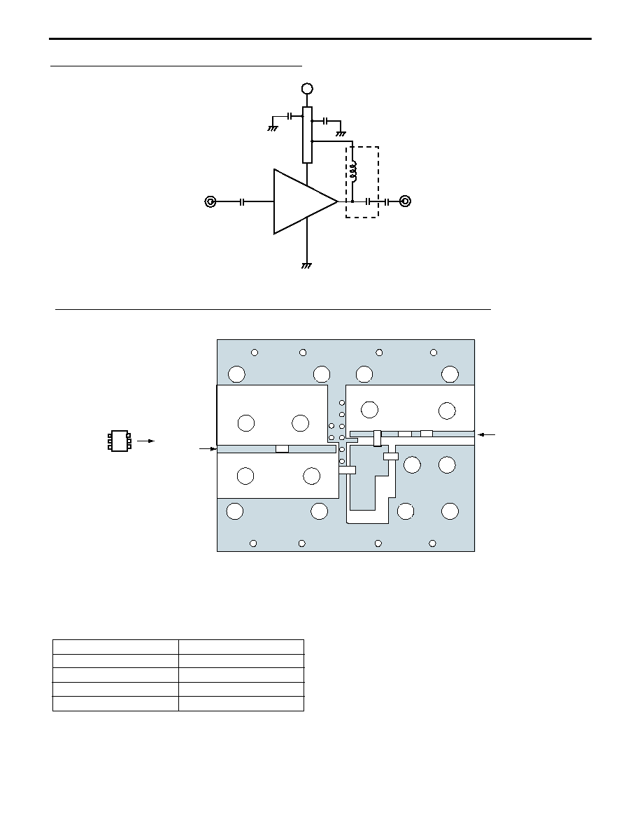
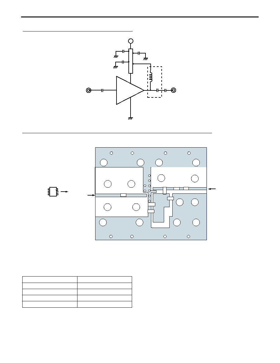
TEST CIRCUIT 3
(f
= 2.4 GHz)
EXAMPLE OF TEST CIRCUIT 3 ASSEMBLED ON EVALUATION BOARD
UPC8178TB
2.4 GHz Output Port Matching
C
1
, C
3
, C
4
, C
5
1000 pF
C
3
10 pF
L
1
1.8 nH
L
2
2.7 nH
COMPONENT LIST
V
CC
C
3
C
4
C
1
C
5
C
2
1
6
4
L
1
L
2
Output port matching circuit
50
OUT
50
IN
2, 3, 5
C3B
Connector
Top View
Mounting direction
AMP . 4
Connector
C
1
IN
L
1
L
2
C
4
C
5
C
3
C
2
OUT
f = 2.4 GHz
NOTES:
1. 42 x 35 x 0.4 mm double sided copper clad polyimide board.
2. Solder plated on pattern.
3. Back side: GND pattern.
4. Through holes.