 | –≠–ª–µ–∫—Ç—Ä–æ–Ω–Ω—ã–π –∫–æ–º–ø–æ–Ω–µ–Ω—Ç: CH7203 | –°–∫–∞—á–∞—Ç—å:  PDF PDF  ZIP ZIP |
201-0000-031 Rev 2.0, 6/2/99
1
CH7203
CHRONTEL
MPEG to TV Encoder with 16-bit Input
Features
∑ Outputs to NTSC, PAL (B, D, G, H, I) and PAL-60
∑ 16-bit YCrCb (4:2:2) input format
∑ Simultaneous composite/S-video outputs
∑ Triple 9-bit video DACs
∑ 27 MHz DAC operating frequency eliminates
the need for 1/sinc(x) correction filter
∑ Low-jitter phase-locked loop circuitry operates
using a low-cost 14.31818 MHz crystal
∑ 40.5 or 33.9 MHz video decoder clock output
∑ 16.934 or 11.289 MHz audio decoder clock output
∑ 13.5 MHz and 27 MHz video pixel clock outputs
∑ Optimized luminance and chrominance internal
filters for NTSC and PAL
∑ HSYNC* and VSYNC* outputs for
master mode operation
∑ Sleep mode
∑ CMOS technology in 44-pin PLCC
∑ 5V single-supply operation
Description
The CH7203 video encoder integrates a dual PLL clock
generator and a digital NTSC/PAL video encoder. By
generating all essential clock signals for MPEG
playback, and converting digital video inputs to either
NTSC or PAL video signals, the CH7203 is an essential
component of any low-cost solution for video-CD
playback machines.
The CH7203 dual PLL clock synthesizer generates all
clocks and timing signals from a 14.31818 MHz
reference crystal (see application note 19 "Tuning
Clock Outputs" for selection and tuning of the 14.31818
MHz crystal). The CH7203 generates a 40.5 or 33.9
MHz video decoder clock, 13.5 MHz and 27 MHz
video pixel clocks, and a 16.934 or 11.289 MHz audio
decoder clock. Timing signals from the PLLs are used
to generate the horizontal and vertical sync signals
which enable operating the CH7203 in master mode.
The fully digital video encoder is pin-programmable to
generate either a 525-line NTSC or a 625-line PAL
compatible video signal. It also features a logic
selectable sleep mode which turns the encoder off while
leaving both PLL's running.
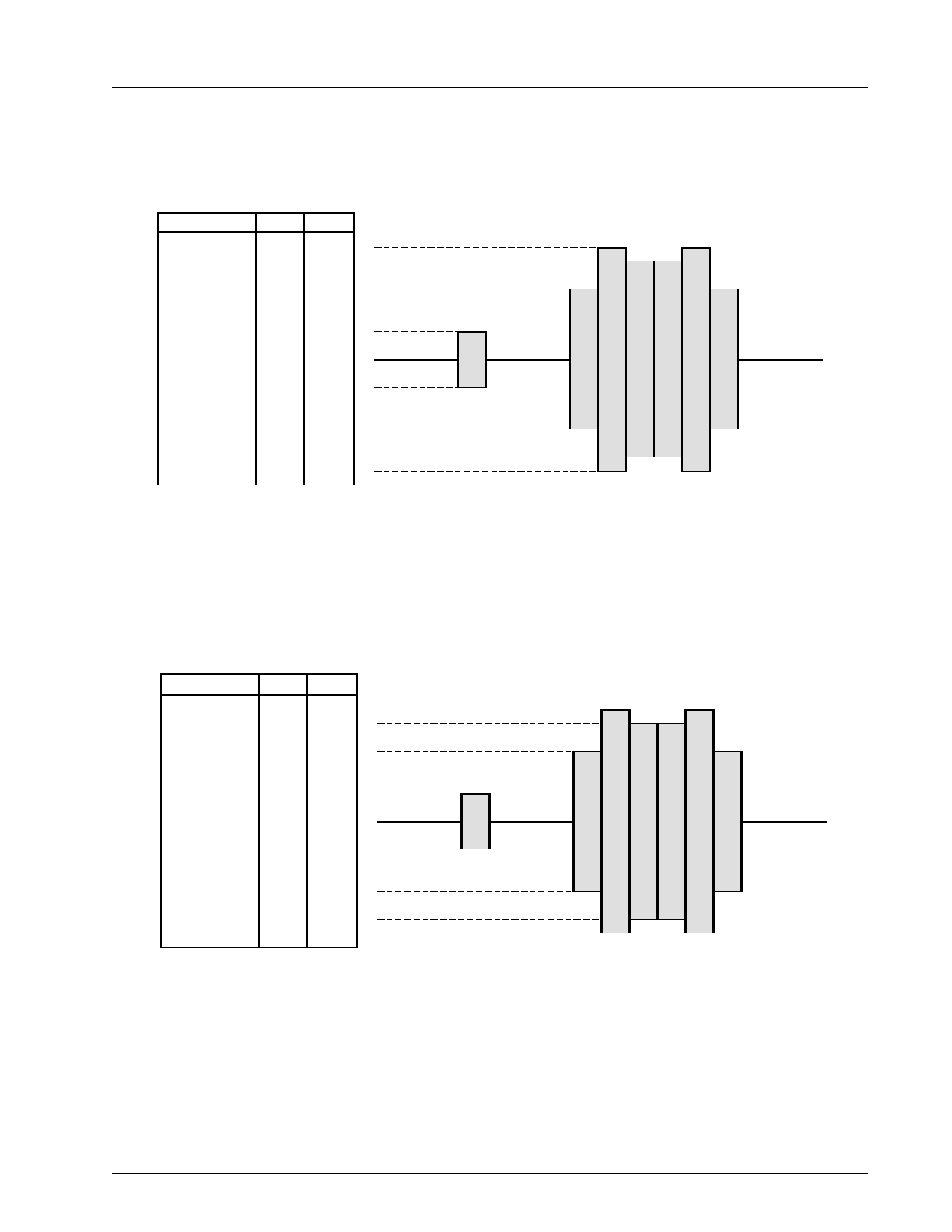
Figure 1: Functional Block Diagram
U
FILTER
V
FILTER
DAC
DAC
DAC
X
M
U
X
M
U
X
M
U
X
Y
FILTER
B LA NKIN G
COL O R-B URST
CO NT RO L
BL AN KING
H ,V SYNC
GEN ERATO R
X
S IN + COSINE
GENERATOR
ACLK
PCLK
Y
CVBS
C
Y[7:0],
IREF
RSET
AVDD
VDD
AGND
GND
XI
XO/FIN
MOD0
MOD1
FS
L INE AR
INTE RP OLATO R
I NTE RFACE
PLL1
S TAT E
M ACHI NE
OSC
PLL2
2XPCLK
DCLK
HSYNC*
VSYNC*
16
9
9
9
CRS
CRSEN*
C[7:0]
1/ 2

CHRONTEL
CH7203
2
201-0000-031 Rev 2.0, 6/2/99
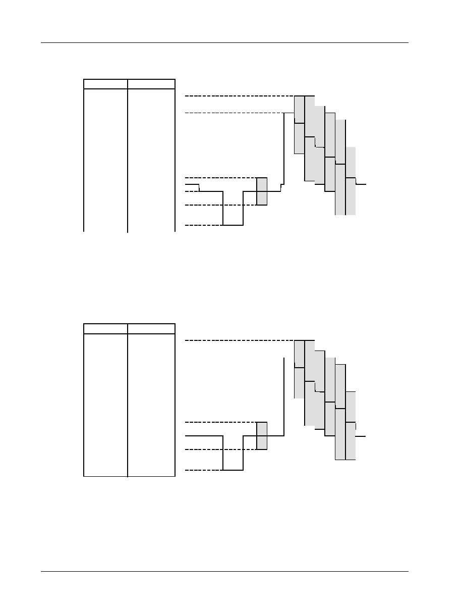
Figure 2: CH7203 Pinout Diagram
MOD0
VSYNC*
HSYNC*
GND
C[1]
CRSEN*
FS
C[6]
MOD1
CRS
C[7]
GND
Y
CVBS
C[5]
C[4]
C[3]
C[2]
VDD
C
AVDD
PCLK
AG
N
D
XI
VD
D
AC
LK
GN
D
2XPC
L
K
VD
D
X
O
/F
IN
DC
LK
GN
D
AV
DD
R
SET
C[
0
]
Y[7]
Y[3]
Y[6]
Y[5]
Y[4]
Y[2]
Y[1]
Y[0]
AG
N
D
7
8
9
10
13
12
11
39
38
37
36
35
14
15
16
17
34
33
32
31
30
29
6
5
4
3
2
1
44
43
42
41
40
18
19
20
21
24
23
22
25
26
27
28
CHRONTEL
CH7203
CHRONTEL
CH7203
201-0000-031 Rev 2.0, 6/2/99
3
Note:
1.
Please refer to crystal manufacturer specifications for proper load capacitances. The optional variable tuning capacitor is
required only if the crystal oscillation frequency cannot be controlled to the required accuracy. The capacitance value for the tuning capac-
itor should be obtained from the crystal manufacturer. For further information, request a copy of Application Note AN-19, "Tuning Clock
Outputs."
Table 1. Pin Descriptions
Pin
Type
Symbol
Description
1
Out
ACLK
Audio Decoder Clock Output
16.934 MHz or 11.289 MHz clock output (selectable by FS) for
MPEG audio decoder operation. The output swing is 5V.
2, 36, 42
Power
VDD
Digital Supply Voltage
These pins supply the 5V power to the digital section of the
CH7203.
3
In
XO/FIN
Crystal Output or External F
REF
Input
1
A 14.31818 MHz (±
50 ppm) parallel resonance crystal may be
attached between XO/FIN and XI. An external CMOS compatible
clock can be connected to XO/FIN as an alternative.
4
In
XI
Crystal Input
1
A 14.31818 MHz (±
50 ppm) parallel resonance crystal should be
attached between XI and XO/FIN. However, if an external CMOS
clock is attached to XO/FIN, XI should be connected to ground.
5, 27
Power
AGND
Analog ground
These pins provide the ground reference for the analog section of
the CH7203. These pins MUST be connected to the system
ground to prevent latchup.
6,29
Power
AVDD
Analog Supply Voltage
These pins supply the 5V power to the analog section of the
CH7203.
7
In
CRSEN*
Cr Select Enable. Internally pulled-up.
CRSEN*=0, Cr, Cb data sequence is specified by the CRS pin.
CRSEN*=1, Cr, Cb data sequence is specified by the CH7203's
internal default condition: Horizontal count = even, data is Cb;
data is Cr otherwise. State of CRS is ignored when CRSEN*=1.
See Figure 6 on page 7.
8
In
FS
Frequency Select. Internally pulled-up
FS = 1 (default), then DCLK = 40.5 MHz, ACLK = 16.934 MHz
FS = 0, then DCLK = 33.9 MHz, ACLK = 11.289 MHz
9
In
MOD1
Mode bit 1 - Internally pulled-up
This input works in conjunction with the MOD0 input to select
NTSC, PAL, or Sleep mode functions. Refer to Table 3, "Video
Encoder Modes," on page 6 for details.
10
In
CRS
Cr Select.
When CRSEN*=0, CRS specifies the CrCb data sequence. CRS
is an alternating signal. CRS=1 indicates that C[7:0] carry the Cr
data. C[7:0] carry the Cb data otherwise. See Figure 7 on page 8.
11 ≠ 18
In
C[7:0]
Video Input
These pins accept the "CrCb" data of the YCrCb (4:2:2) digital
video format. The Cb & Cr data appear alternately. The sequence
of the Cb, Cr data is either predefined by the internal horizontal
counter (even = Cb, odd = Cr) or as specified by pin CRS (data is
Cr for CRS=1 and Cb otherwise. For more details, please refer to
the timing diagram shown in Figure 6 on page 7.
Cb & Cr have a nominal range of 16≠240, with 128 equal to zero.

CHRONTEL
CH7203
4
201-0000-031 Rev 2.0, 6/2/99
Table 2. Pin Descriptions (continued)
Pin
Type
Symbol
Description
19-26
In
Y[7:0]
Video Input
These pins accept the "Y" data of the YCrCb (4:2:2) digital video
format. For more details, please refer to the timing diagram
shown in Figure 7 on page 8. Y has a nominal range of 16-235.
28
In
RSET
Reference Resistor
A 360
resistor with short and wide traces should be attached
between RSET and ground. No other connections should be
made to this pin.
30
Out
C
Chrominance Output
A 75
termination resistor with short traces should be attached
between C and ground for optimum performance.
31
Out
CVBS
Composite Output
A 75
termination resistor with short traces should be attached
between CVBS and ground for optimum performance.
32
Out
Y
Luminance Output
A 75
termination resistor with short traces should be attached
between Y and ground for optimum performance.
33, 34, 40, 44
Power
GND
Digital Ground
These pins provide the ground reference for the digital section of
the CH7203. These pins MUST be connected to the system
ground through independent ground vias.
35
Out
HSYNC*
Horizontal Sync Output
The horizontal sync output is generated by the CH7203 for master
mode operation. HSYNC* is an active low signal with a 5V output
swing. For additional information, please refer to the timing
diagrams shown in Figures 5 and 6 on page 7.
37
Out
VSYNC*
Vertical Sync Output
The vertical sync output is generated by the CH7203 for master
mode operation. VSYNC* is an active low signal with a 5V output
swing. For additional information, please refer to the timing
diagrams shown in Figures 5 and 7 on page 7 and 8.
38
In
MOD0
Mode bit 0 - internally pulled-up
This input works in conjunction with the MOD1 input to select
NTSC, PAL, or Sleep Mode functions. Refer to Table 3, "Video
Encoder Modes," on page 6 for details.
39
Out
PCLK
Video Pixel Clock Output
13.5 MHz clock output. The output swing is 5V.
41
Out
DCLK
MPEG Decoder Clock Output
40.5 MHz or 33.9 MHz clock output (selectable by FS). The output
swing is 5V.
43
Out
2XPCLK
Double Pixel Clock Output
27 MHz clock output. The output swing is 5V.

CHRONTEL
CH7203
201-0000-031 Rev 2.0, 6/2/99
5
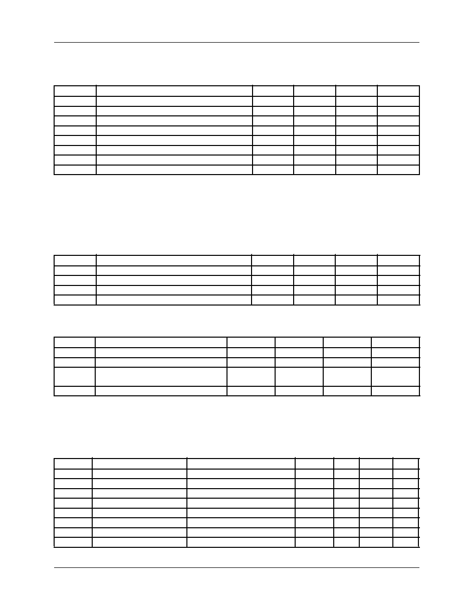
Figure 3: CH7203 Interface Diagram
Note:
1.
Please refer to the Optional Output Filter diagram below
2. The proper value of these capacitors depends on the crystal manufacturer's specifications. Please refer to AN06 for the
details of the calculation.
Figure 4: Optional Output Filter
14.318
MHz
XI
XO/FIN
3
75
Y
C
CVBS
S-
Vi
d
e
o
Co
n
n
e
c
t
o
r
CH7203
Ferrite Bead
1
32
75
Ferrite Bead
1
30
75
Ferrite Bead
1
31
360
RSET
28
C
o
m
pos
i
t
e
C
onne
c
t
or
4
MPEG Decoder
and
System Controller
8
C[7:0]
ACLK
DCLK
2XPCLK
VSYNC*
HSYNC*
11 - 18
1
41
43
37
35
27 pF
2
27 pF
2
FS
JUMPER
CRSEN
CRS
8
10
7
PCLK
39
MOD1
9
MOD0
38
Y[7:0]
8 19-26
75
1.2uH
47 pF
1.2uH
270 pF
150 pF
Y, C, CVBS
OUTPUT

CHRONTEL
CH7203
6
201-0000-031 Rev 2.0, 6/2/99
General Description
The CH7203 is a fully integrated solution for converting 16-bit YCrCb (4:2:2) digital video inputs into high-
quality NTSC or PAL video signals while generating all essential clock signals for MPEG playback. All
essential circuitry for this conversion and clock generation (Dual PLL's, linear interpolator, digital filters,
NTSC/PAL encoder, DAC's) are contained in the CH7203 making it an essential component of any low-cost
solution for video-CD playback machines. Refer to the Block Diagram on page 1 and the Interface Diagram on
page 5.
Functional Description
The encoded luminance (Y) and color-difference (U,V) are interpolated, and filtered through digital filters to
minimize aliasing problems. The filtered signals go to the digital encoder where they are transformed to
composite and S-video outputs, and then they are converted by the three 9-bit DACs to analog outputs.
16-bit YCrCb (4:2:2) Input
Y data is input through the Y[7:0] inputs and CrCb data is multiplexed through the C[7:0] inputs. When
CRSEN* = 1, the Cr Select input, CRS, is ignored, and all even horizontal pixels are Cb data and all odd
horizontal pixels are Cr. Refer to Figure 6 on page 7 for the definition of "even" and "odd" pixels. When
CRSEN* = 0, the alternating CRS signal specifies the CrCb sequence. CRS = 1 indicates C[7:0] carries Cr
data, and CRS = 0 indicates C[7:0] carries Cb data.
Clock/Data/Synchronization Timing
The CH7203 not only works as an NTSC/PAL encoder, it also supplies the necessary clocks (1X pixel, 2X
pixel, video system, and audio) and synchronization (HSYNC* and VSYNC*) signals to other building blocks
in the video system. For this reason, the CH7203 works only in the Master mode.
It is important to note the CH7203 does not have a "pixel clock" input pin. Therefore, the timing issues related
to video pixel data being supplied from, for example, the MPEG decoder, to the CH7203 (pins Y[7:0] and
C[7:0]) need to be clarified. Assume the pixel synchronization of a system is based on the 2X pixel clock
(2XPLCK). In this type of design, 2XPCLK is distributed across the entire video system, and it is also used to
latch the incoming data appearing at pins Y[7:0] and C[7:0]. Figure 7 on page 8 shows all timing referenced
to the 2XPCLK output signal (loaded with 50pF).
Video Encoder Modes
Combinations of the two signals MOD1 and MOD0 select the various power saving modes as shown below.
Table 3 ∑ Video Encoder Modes
Frequency Select Modes
The frequency select input FS affects the DCLK and ACLK outputs as shown below:
FS = 1 (default) DCLK = 40.5 MHz, ACLK = 16.934 MHz
FS = 0
DCLK = 33.9 MHz, ACLK = 11.289 MHz
MOD1
MOD0
Video Encoder Mode
1
1
NTSC
1
0
PAL
0
1
PAL-60
0
0
Sleep mode (Encoder off,both PLLs running)

CHRONTEL
CH7203
201-0000-031 Rev 2.0, 6/2/99
7
Timing Diagrams
Figure 5: HSYNC* and VSYNC* Timing
Figure 6: Cb, Cr Sequence Diagram
VSYNC*
VSYNC*
t
7
t
7
E
VE N
F
IE LD
M
AS T E R
M
ODE
O
DD
F
I E LD
M
A S T ER
M
ODE
HSYNC*
2XPCLK
(out)
Y
(in)
C
(in)
HSYNC*
(out)
64 2XPCLK cycles
t10
Cr
Cb
Cr
PCLK
(out)
Pixel[1]
Pixel[2]
First (Y,C) data latched in after HSYNC* goes low
Pixel[0]
Cb

CHRONTEL
CH7203
8
201-0000-031 Rev 2.0, 6/2/99
Figure 7: Clock/Data/Synchronization Timing Diagram
Note: Refer to Table 8 on page 14 for timing values
Figure 8: Interlaced NTSC Timing Diagram
2XPCLK
PCLK
H/V Sync
Data is latched into the device on the falling edge of 2XPCLK, when PCLK is low.
t
5
Pixel Data
t
3
t4
t
6
t
1
t
2
Latch
Latch
Latch
520
521
522
523
524
525
1
2
3
4
5
6
7
258
259
260
261
262
263
264
265
266
267
268
269
272
START
OF
VSYNC
ANALOG
FIELD 1
ANALOG
FIELD 2
8
9
270
271
520
521
522
523
524
525
1
2
3
4
5
6
7
258
259
260
261
262
263
264
265
266
267
268
269
272
START
OF
VSYNC
ANALOG
FIELD 1
ANALOG
FIELD 2
8
9
270
271
520
521
522
523
524
525
1
2
3
4
5
6
7
258
259
260
261
262
263
264
265
266
267
268
269
272
START
OF
VSYNC
ANALOG
FIELD 1
ANALOG
FIELD 2
8
9
270
271
Pre-equaliz ing
pulse vertica
l
Reference
sub- car rier phase
color field 1
Line
vertic al
interv al
Ver tical sync
pulse interva
l
P os t- equalizing
pulse interval
S tart of
field 1
S tart of
field 2
Reference
sub-carrier phase
color field 2
Reference
sub- carrier phase
color field 3
Reference
sub-c arr ier phas e
c olor field 4
S tart of
field 3
Start of
field 4
t
1
+V
t
2
+V
t
3
+V
523
524
525
1
2
3
4
5
6
7
8
9
10
11
12
261
262
263
264
265
266
267
268
269
270
271
272
273
274
275
523
524
525
1
2
3
4
5
6
7
8
9
10
11
12
261
262
263
264
265
266
267
268
269
270
271
272
273
274
275
CHRONTEL
CH7203
201-0000-031 Rev 2.0, 6/2/99
9
Figure 9: Interlaced PAL Timing Diagram
621
622
623
624
625
1
2
3
4
5
6
7
620
621
622
623
624
625
1
2
3
4
5
6
7
620
309
310
311
312
313
314
315
316
317
318
319
320
323
308
322
309
310
311
312
313
314
315
316
317
318
319
320
308
START
OF
VSYNC
ANALOG
FIELD 1
ANALOG
FIELD 2
ANALOG
FIELD 3
ANALOG
FIELD 4
BURST
BLANKING
PAL SWITCH = 0, +V COMPONENT
BURST PHASE = REFERENCE PHASE = 135 RELATIVE TO U
∞
PAL SWITCH = 1, - V COMPONENT
BURST PHASE = REFERENCE PHASE + 90 = 225 RELATIVE TO U
∞
∞
8
9
10
321
8
9
10
323
322
321
621
622
623
624
625
1
2
3
4
5
6
7
620
621
622
623
624
625
1
2
3
4
5
6
7
620
309
310
311
312
313
314
315
316
317
318
319
320
323
308
322
309
310
311
312
313
314
315
316
317
318
319
320
308
START
OF
VSYNC
ANALOG
FIELD 1
ANALOG
FIELD 2
ANALOG
FIELD 3
ANALOG
FIELD 4
BURST
BLANKING
PAL SWITCH = 0, +V COMPONENT
BURST PHASE = REFERENCE PHASE = 135 RELATIVE TO U
∞
PAL SWITCH = 1, - V COMPONENT
BURST PHASE = REFERENCE PHASE + 90 = 225 RELATIVE TO U
∞
∞
8
9
10
321
8
9
10
323
322
321
INTE RVA LS
4
3
2
1
CHRONTEL
CH7203
10
201-0000-031 Rev 2.0, 6/2/99
Figure 10: NTSC Y (Luminance) Output Waveform
Figure 11: PAL Y (Luminance) Video Output Waveform
COLOR BARS :
White
Yellow
Cyan
Green
Magenta
Red
Blue
Black
Blank
Color / Level
mA
V
Sync
24.60
22.85
19.85
18.11
13.49
10.49
8.74
7.49
0.50
15.23
0.922
0.857
0.745
0.679
0.506
0.393
0.327
0.281
0.019
0.571
Note: 1 100% amplitude, 100% saturation color bars are shown
Note: 2 Vref = 1.235V, RSET = 360
, 75
doubly terminated load
26.59
24.59
21.30
19.30
16.15
14.15
11.00
9.00
7.58
0.00
0.997
0.922
0.799
0.724
0.606
0.531
0.413
0.338
0.284
0.000
COLOR BARS :
White
Yellow
Cyan
Green
Magenta
Red
Blue
Black
Blank
Color / Level
mA
V
Sync
24.60
22.85
19.85
18.11
13.49
10.49
8.74
7.49
0.50
15.23
0.922
0.857
0.745
0.679
0.506
0.393
0.327
0.281
0.019
0.571
Note: 1 100% amplitude, 100% saturation color bars are shown
Note: 2 Vref = 1.235V, RSET = 360
, 75
doubly terminated load
26.83
24.69
19.05
21.19
15.70
13.57
10.21
8.08
0.00
1.006
0.926
0.795
0.715
0.589
0.509
0.383
0.303
0.000
Blank
CHRONTEL
CH7203
201-0000-031 Rev 2.0, 6/2/99
11
Figure 12: NTSC C (Chrominance) Video Output Waveform
Figure 13: PAL C (Chrominance) Video Output Waveform
COLOR BARS :
3.579545 MHz Color Burst
(9 cycles)
Cyan / Red
Green / Magenta
Yellow / Blue
Peak Burst
Blank
Peak Burst
Yellow / Blue
Green / Magenta
Cyan / Red
22.60
21.85
19.61
15.98
12.49
8.99
5.37
3.12
2.37
0.848
0.819
0.735
0.599
0.468
0.337
0.201
0.117
0.089
Color / Level
mA
V
Note: 1 100% amplitude, 100% saturation color bars are shown
Note: 2 Vref = 1.235V, RSET = 360
, 75
doubly terminated load
25.37
24.59
22.16
18.15
14.294
10.44
6.43
4.00
3.21
0.951
0.922
0.831
0.681
0.536
0.391
0.241
0.150
0.121
COLOR BARS :
4.433619 MHz Color Burst
(10 cycles)
Cyan / Red
Green / Magenta
Yellow / Blue
Peak Burst
Blank
Peak Burst
Yellow / Blue
Green / Magenta
Cyan / Red
16.23
12.49
8.74
0.609
0.468
0.328
Color / Level
mA
V
22.60
21.85
19.61
5.37
3.12
2.37
0.848
0.819
0.735
0.201
0.117
0.089
Note: 1 100% amplitude, 100% saturation color bars are shown
Note: 2 Vref = 1.235V, RSET = 360
, 75
doubly terminated load
27.06
26.22
23.63
19.21
15.24
11.28
6.85
4.27
3.43
1.015
0.983
0.886
0.720
0.572
0.423
0.257
0.160
0.129
CHRONTEL
CH7203
12
201-0000-031 Rev 2.0, 6/2/99
Figure 14: Composite NTSC Video Output Waveform
Note:
Vref = 1.235V, RSET = 360
, 75
doubly terminated load
Figure 15: Composite PAL Video Output Waveform
Note:
Vref = 1.235V, RSET = 360
, 75
doubly terminated load
COLOR BARS :
WHI
T
E
YE
LLOW
CY
A
N
GR
E
E
N
MA
G
E
NT
A
RE
D
BLU
E
BLA
C
K
3.579545 MHz
Color Burst
(9 Cycles)
Peak Chroma
Peak Burst
Black
Color / Level
mA
V
Sync
33.89
27.37
9.62
4.32
0.50
12.00
1.271
1.026
0.360
0.162
0.019
0.450
Blank
8.16
0.306
White
Peak Burst
32.45
26.59
11.43
9.00
7.58
3.72
0.00
1.217
0.997
0.429
0.338
0.284
0.139
0.000
4.433619 MHz
Color Burst
(10 Cycles)
COLOR BARS :
WHI
T
E
YE
LLOW
CY
A
N
GR
E
E
N
MA
G
E
NT
A
RE
D
BLU
E
BLA
C
K
Peak Chroma
Peak Burst
Color / Level
mA
V
Sync
33.89
27.37
4.58
0.50
12.00
1.271
1.026
0.171
0.019
0.450
Blank/Black
8.64
0.324
White
Peak Burst
33.08
26.83
12.04
8.08
4.12
0.00
1.240
1.006
0.452
0.303
0.154
0.000
CHRONTEL
CH7203
201-0000-031 Rev 2.0, 6/2/99
13
Electrical Specifications
Table 4 ∑ Absolute Maximum Ratings
Note:
Stresses greater than those listed under absolute maximum ratings may cause permanent damage to the device. These are
stress ratings only. Functional operation of the device at these or any other conditions above those indicated under the normal
operating conditions is not recommended. Exposure to absolute maximum rating conditions for extended periods may affect
reliability.
The device is fabricated using high-performance CMOS technology. It should be handled as an ESD-sensitive device.
Voltage on any signal pin that exceeds the power supply voltage by more than +0.5V can induce destructive latchup.
Table 5 ∑ Recommended Operating Conditions
Table 6 ∑ Electrical Characteristics (Operating Conditions: T
A
= 0∞C ≠ 70∞C, V
DD
= 5V ± 5%)
Note:
As applied to Tables 4, 5, and 6, Recommended Operating Conditions are used as test conditions unless otherwise specified.
RSET = 360
,
and NTSC CCIR601 operation. Typical values are based on 25
∞
C and +5V.
Table 7 ∑ Digital Inputs / Outputs
Symbol
Description
Min
Typ
Max
Units
VDD relative to GND
- 0.5
7.0
V
Input voltage of all digital pins
1
GND - 0.5
V
DD
+ 0.5
V
T
SC
Analog output short circuit duration
Indefinite
Sec
T
AMB
Ambient operating temperature
- 55
125
∞
C
T
STOR
Storage temperature
- 65
150
∞
C
T
J
Junction temperature
150
∞
C
T
VPS
Vapor phase soldering (one minute)
220
∞
C
P
MAX
Maximum power dissipation
TBD
W
Symbol
Description
Min
Typ
Max
Units
AVDD
Analog supply voltage
5.00
DVDD
Digital supply voltage
5.00
T
A
Ambient operating temperature
0
25
70
∞
C
R
L
Output load to DAC outputs
37.5
Symbol
Description
Min
Typ
Max
Unit
Video D/A resolution
9
9
9
Bits
Full scale output current
33.08
mA
Video level error
using internal reference
10
%
Total Current Consumption
135
mA
Symbol
Description
Test Condition @ T
A
= 25∞C
Min
Typ
Max
Units
V
OH
Output high voltage
I
OH
=
-
400
µ
A
2.4
V
V
OL
Output low voltage
I
OL
= 3.2 mA
0.4
V
V
IH
Input high voltage
2.0
V
DD
+ 0.5
V
V
IL
Input low voltage
GND - 0.5
0.8
V
I
PU
Input internal pull-up current
5
25
µ
A
I
LK
Input leakage current
-10
10
µ
A
CD
IN
Input capacitance
f = 1 MHz,
V
IN
= 2.4V
7
pF
CD
OUT
Output capacitance
10
pF

CHRONTEL
CH7203
14
201-0000-031 Rev 2.0, 6/2/99
Electrical Specifications (continued)
Table 8 ∑ AC Characteristics
Symbol
Description
Min
Typ
Max
Units
t
1
2XPCLK
37
ns
t
2
2XPCLK high time
14.8
22.2
ns
t
3
Pixel/Sync setup time
6
ns
t
4
Pixel/Sync hold time
3
ns
t
5
Sync active delay time
3
ns
t
6
Sync inactive delay time
17
ns
t
7
HSYNC* to VSYNC* delay
30
30
ns
t
10
HSYNC* pulse width
64 x t
1
ns
VSYNC* delay time
17
20
ns
VSYNC* pulse width
2.0
Hor. lines
Test
Conditions:
Unless otherwise specified, the testing conditions are the same as in Table 5, "Recommended Operating Conditions,"
on page 13. TTL input values are 0 ≠ 3V, with input rise / fall times < 3 ns, measured between the
V
IL
and
V
IH
. Timing
reference points at 50% for non-TTL inputs and outputs. TTL reference points at 1.5V for inputs and outputs. Analog
output load < 10 pF.
Since the CH7203 does not have a pixel clock input, all input signal timing is chosen with respect to the output clock
timing of 2XPCLK and PCLK. PCLK can be used at the "Qualifying" clock for certain MPEG decoders.
Chrontel
2210 O'Toole Avenue
San Jose, CA 95131-1326
Tel: (408) 383-9328
Fax: (408) 383-9338
1997 Chrontel, Inc. All Rights Reserved.
Chrontel PRODUCTS ARE NOT AUTHORIZED FOR AND SHOULD NOT BE USED WITHIN LIFE SUPPORT SYSTEMS OR NUCLEAR FACILITY APPLICATIONS WITHOUT THE
SPECIFIC WRITTEN CONSENT OF Chrontel. Life support systems are those intended to support or sustain life and whose failure to perform when used as directed can reasonably
expect to result in personal injury or death. Chrontel reserves the right to make changes at any time without notice to improve and supply the best possible product and is not
responsible and does not assume any liability for misapplication or use outside the limits specified in this document. We provide no warranty for the use of our products and assume no
liability for errors contained in this document. Printed in the U.S.A.
ORDERING INFORMATION
Part number
Package type
Number of pins
Voltage supply
CH7203-V
PLCC
44
5V
CHRONTEL
CH7203
15
201-0000-031 Rev 2.0, 6/2/99