CH7304
Brief Datasheet
209-0000-034
Rev. 1.1, 5/15/2003
1
Chrontel
Chrontel CH7304 Single LVDS Transmitter
Features 1.0
General
Description
∑ Single LVDS transmitter
∑ Supports pixel rate up to 100M pixels/sec
∑ Supports up to SXGA resolution (1280 x 1024)
∑ LVDS low jitter PLL
∑ LVDS 24-bit or 18-bit output
∑ 2D dither engine for 18-bit output
∑ Panel protection and power down sequencing
∑ Programmable power management
∑ Fully programmable through serial port
∑ Complete Windows and DOS driver support
∑ Variable voltage interface to graphics device
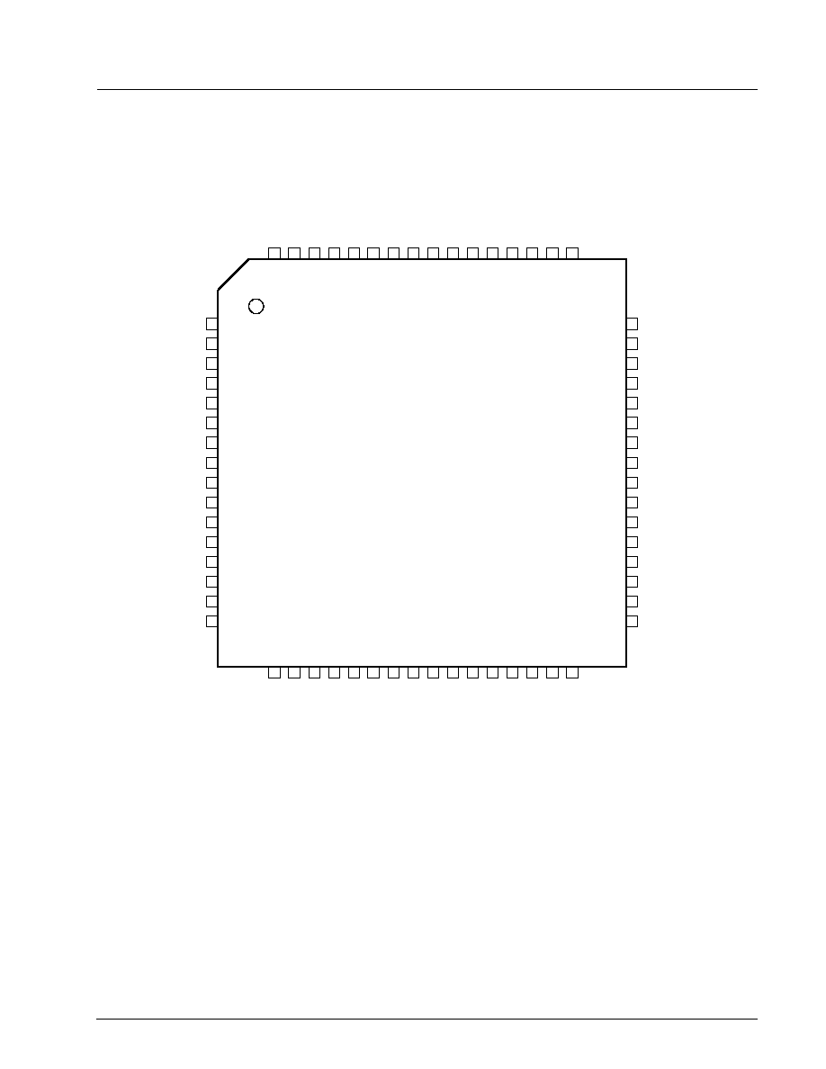
∑ Offered in a 64-pin LQFP package
The CH7304 is a Display Controller device, which accepts
a graphics data stream over one 12-bit wide variable
voltage (1.1V to 3.3V) port. The data stream outputs
through an LVDS transmitter to an LCD panel. A
maximum of 100M pixels per second can be output
through a single LVDS link.
The LVDS transmitter supports 24-bit panels; it also
includes a programmable dither function for support of
18-bit panels. Data is encoded into commonly used
formats, including those detailed in the OpenLDI and the
SPWG specification. Serialized data output on four
differential channels.
VREF
GP
I
O
R
E
SET
*
XI/FIN,XO
LVDS PLL
Dither
Engine
LVDS
Transmit
Clock,
Data,
Sync
Latch &
Demux
LVDS
Encode /
Serialize
D
a
ta
M
u
x
/
Fo
rm
a
t
XCLK,XCLK*
D[11:0]
H,V, DE
3
12
2
Serial Port Control and Misc. Functions
SP
C
SP
D
LDC[7:4],LDC*[7:4]
LL1C,LL1C*
LDC[3:0],LDC*[3:0]
LL2C, LL2C*
XTAL
6
2
6
2
2
2
ENAVDD, ENABKL
Color
Space
Conversion
Figure 1: Functional Block Diagram

CHRONTEL
CH7304
209-0000-034
Rev. 1.1, 5/15/2003
3
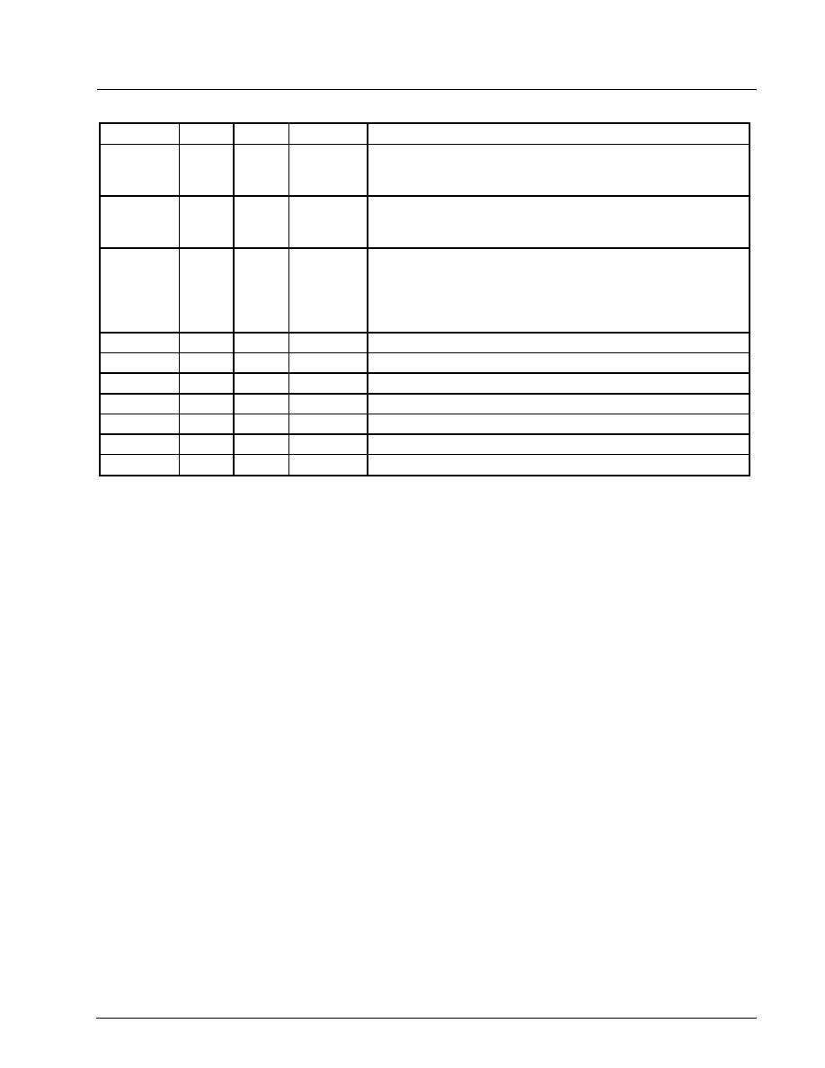
2.2 Pin Description
Table 1: Pin Description
Pin #
# of Pins Type
Symbol
Description
1 1
Out
ENABLK
Back Light Enable
Enable Back-Light of LCD Panel. Output is driven from 0 to DVDD.
2 1
Out
ENAVDD
Panel Power Enable
Enable panel VDD. Output is driven from 0 to DVDD.
3,4,6,7,9,10,
12,13,15,16
10 -
NC No Connect
20, 21
2
Out
LLC, LLC*
LVDS Differential Clock
17,23,26,29 4
Out LDC[3:0] Positive LVDS differential data[3:0]
18,24,27,30 4
Out LDC[3:0]* Negative LVDS differential data [3:0]
32 1
In
VSWING
LVDS Voltage Swing Control
This pin sets the swing level of the LVDS outputs. A 2.4K Ohm resistor
should be connected between this pin and LGND (pin 31) using short and
wide traces.
33 1
Out
XO
Crystal Output
A parallel resonance 14.31818MHz crystal (+ 20 ppm) should be attached
between this pin and XI. However, if an external CMOS clock is attached
to XI, XO should be left open.
34 1
In
XI Crystal Input / External Reference Input
A parallel resonance 14.31818MHz crystal (+ 20 ppm) should be attached
between this pin and XO. However, an external CMOS compatible clock
can drive the XI input.
37 1
Analog
LPLL_CAP
LVDS PLL Capacitor
This pin allows coupling of any signal to the on-chip loop filter capacitor.
39 1
In/Out
GPIO
General Purpose Input / Output
This pin provides general purpose I/O and is controlled via the serial port.
The voltage level on input and output is DVDD. See description of GPIO
Controls for I/O configuration.
40 1
In
SPC
Serial Port Clock Input
This pin functions as the clock input of the serial port and can operate with
inputs from 1.1V ~ 3.3V. The serial port address of the CH7304 is 75h. For
more details on CH7304 serial port read/write operations, please refer to
AN61.
41 1
In/Out
SPD
Serial Port Data Input / Output
This pin functions as the bi-directional data pin of the serial port and can
operate with inputs from 1.1V ~ 3.3V. Outputs are driven from 0 to VDDV.
The serial port address of the CH7304 is 75h. For more details on CH7304
serial port read/write operations, please refer to AN61.
43 1
In
V Vertical Sync Input
This pin accepts a vertical sync input for use with the input data. The
amplitude will be 0 to VDDV. VREF signal is the threshold level.
44 1
In
H Horizontal Sync Input
This pin accepts a horizontal sync input for use with the input data. The
amplitude will be 0 to VDDV. VREF is the threshold level for this input.
45 1
In
VREF
Reference Voltage Input
The VREF pin inputs a reference voltage of VDDV / 2. The signal is
derived externally through a resistor divider and decoupling capacitor, and
will be used as a reference level for data, sync and clock inputs.
46 1
In
DE
Data Enable
This pin accepts a data enable signal which is high when active video data
is input to the device, and remains low during all other times. The levels
are 0 to VDDV. VREF is the threshold level.
CHRONTEL
CH7304
4 209-0000-034
Rev. 1.1,
5/15/2003
Table 1: Pin Description (continued)
Pin #
# of Pins Type
Symbol
Description
47 1
In
RESET*
Reset * Input (Internal Pull-up)
When this pin is low, the device is held in the power on reset condition.
When this pin is high, reset is controlled through the serial port.
50-55, 58-63
12 In D[11:0]
Data[11] through Data[0] Inputs
These pins accept the 12 data inputs from a digital video port of a graphics
controller. The levels are 0 to VDDV. VREF is the threshold level.
56, 57
2
In
XCLK,
XCLK*
External Clock Inputs
These inputs form a differential clock signal input to the device for use with
the H, V and D[11:0] data. If differential clocks are not available, the
XCLK* input should be connected to VREF. The clock polarity can be
selected by the MCP control bit (
Register 1Ch
).
42, 64
2
Power
DVDD
Digital Supply Voltage (3.3V)
35, 49
2
Power
DGND
Digital Ground
48 1
Power
VDDV
I/O Supply Voltage (1.1V to 3.3V)
5,11,22,28 4
Power LVDD
LVDS Supply Voltage (3.3V)
8,14,19,25,31 5
Power LGND
LVDS Ground
38 1
Power
LPLL_VDD
LVDS PLL Supply Voltage (3.3V)
36 1
Power
LPLL_GND
LVDS PLL Ground

CHRONTEL
CH7304
6 209-0000-034
Rev. 1.1,
5/15/2003
Disclaimer
This document provides technical information for the user. Chrontel reserves the right to make changes at any time
without notice to improve and supply the best possible product and is not responsible and does not assume any liability
for misapplication or use outside the limits specified in this document. We provide no warranty for the use of our
products and assume no liability for errors contained in this document. The customer should make sure that they have
the most recent data sheet version. Customers should take appropriate action to ensure their use of the products does not
infringe upon any patents. Chrontel, Inc. respects valid patent rights of third parties and does not infringe upon or assist
others to infringe upon such rights.
Chrontel PRODUCTS ARE NOT AUTHORIZED FOR AND SHOULD NOT BE USED WITHIN LIFE SUPPORT
SYSTEMS OR NUCLEAR FACILITY APPLICATIONS WITHOUT THE SPECIFIC WRITTEN CONSENT OF
Chrontel. Life support systems are those intended to support or sustain life and whose failure to perform when used as
directed can reasonably expect to result in personal injury or death.
Chrontel
2210 O'Toole Avenue, Suite 100,
San Jose, CA 95131-1326
Tel: (408) 383-9328
Fax: (408) 383-9338
www.chrontel.com
E-mail: sales@chrontel.com
2003 Chrontel, Inc. All Rights Reserved.
Printed in the U.S.A.