 | –≠–ª–µ–∫—Ç—Ä–æ–Ω–Ω—ã–π –∫–æ–º–ø–æ–Ω–µ–Ω—Ç: CS61583 | –°–∫–∞—á–∞—Ç—å:  PDF PDF  ZIP ZIP |

Features
∑
Dual T1/E1 Line Interface
∑
Low Power Consumption
(Typically 220mW per Line Interface)
∑
Matched Impedance Transmit Drivers
∑
Common Transmit and Receive Transform-
ers for all Modes
∑
Selectable Jitter Attenuation for Transmit
or Receive Paths
∑
Supports JTAG Boundary Scan
∑
Hardware Mode Derivative of the CS61584
General Description
The CS61583 is a dual line interface for T1/E1 applica-
tions, designed for high-volume cards where low power
and high density are required. Each channel features
individual control and status pins which eliminates the
need for external microprocessor support. The
matched impedance drivers reduce power consumption
and provide substantial return loss to insure superior
T1/E1 pulse quality.
The CS61583 provides JTAG boundary scan to en-
hance system testability and reliability. The CS61583 is
a 5 volt device and is a hardware mode derivative of
the CS61584.
ORDERING INFORMATION
CS61583-IL5: 68-pin PLCC, -40 to +85 ∞C
CS61583-IQ5: 64-pin TQFP, -40 to +85 ∞C
JULY '96
DS172PP5
1
Crystal Semiconductor Corporation
P. O. Box 17847, Austin, Texas, 78760
(512) 445 7222 FAX:(512) 445 7581
Dual T1/E1 Line Interface
TTIP1
TRING1
RRING1
RTIP1
DRIVER
CONTROL
TCLK1
RCLK1
JTAG
4
REFCLK 1XCLK
TV+ TGND RV+ RGND DV+ DGND AV+ AGND BGREF
2
2
2
2
3
2
CLOCK GENERATOR
TPOS1/
TNEG1/
RPOS1/
RNEG1/
LOS1 LOS2
PULSE
SHAPING
CIRCUITRY
CLOCK &
DATA
RECOVERY
LOS
DETECT
TAOS
TTIP2
TRING2
RRING2
RTIP2
DRIVER
TCLK2
RCLK2
TPOS2/
TNEG2/
RPOS2/
RNEG2/
PULSE
SHAPING
CIRCUITRY
CLOCK &
DATA
RECOVERY
TAOS
LOS
DETECT
RESET
CLKE
TAOS1
LLOOP1
RLOOP1
CON01
CON11
CON21
RLOOP2
LLOOP2
TAOS2
CON02
CON12
CON22
AMI2
AMI1
CODER2
CODER1
ATTEN1
ATTEN2
JITTER
ATTENUATOR
E
N
C
O
D
E
R
D
E
C
O
D
E
R
L
O
C
A
L
L
O
O
P
B
A
C
K
R
E
M
O
T
E
L
O
O
P
B
A
C
K
JITTER
ATTENUATOR
E
N
C
O
D
E
R
D
E
C
O
D
E
R
L
O
C
A
L
L
O
O
P
B
A
C
K
R
E
M
O
T
E
L
O
O
P
B
A
C
K
TDATA1
AIS1
RDATA1
BPV1
TDATA2
AIS2
RDATA2
BPV2
RECEIVER
RECEIVER
CS61583
Copyright
©
Crystal Semiconductor Corporation 1996
(All Rights Reserved)

Table of Contents
Block Diagram . . . . . . . . . . . . . . . . . . . . . . . . . . . . . . . . . . . . . . . . . 1
Specifications
Absolute Maximum Ratings . . . . . . . . . . . . . . . . . . . . . . . . . 3
Recommended Operating Conditions. . . . . . . . . . . . . . . . . . 3
Digital Characteristics. . . . . . . . . . . . . . . . . . . . . . . . . . . . . . 4
Analog Specifications
Receiver . . . . . . . . . . . . . . . . . . . . . . . . . . . . . . . . . . 4
Jitter Attenuator . . . . . . . . . . . . . . . . . . . . . . . . . . . . 4
Transmitter . . . . . . . . . . . . . . . . . . . . . . . . . . . . . . . . 5
Switching Characteristics
T1 Clock/Data. . . . . . . . . . . . . . . . . . . . . . . . . . . . . . 6
E1 Clock/Data. . . . . . . . . . . . . . . . . . . . . . . . . . . . . . 6
JTAG. . . . . . . . . . . . . . . . . . . . . . . . . . . . . . . . . . . . . 8
General Description
Overview. . . . . . . . . . . . . . . . . . . . . . . . . . . . . . . . . . . . . . . . 9
Transmitter . . . . . . . . . . . . . . . . . . . . . . . . . . . . . . . . . . . . . . 10
Receiver . . . . . . . . . . . . . . . . . . . . . . . . . . . . . . . . . . . . . . . . 12
Jitter Attenuator . . . . . . . . . . . . . . . . . . . . . . . . . . . . . . . . . . 12
Reference Clock . . . . . . . . . . . . . . . . . . . . . . . . . . . . . . . . . . 13
Power-Up Reset . . . . . . . . . . . . . . . . . . . . . . . . . . . . . . . . . . 13
Line Control and Monitoring . . . . . . . . . . . . . . . . . . . . . . . . 13
Line Code Encoder/Decoder. . . . . . . . . . . . . . . . . . . 13
Alarm Indication Signal . . . . . . . . . . . . . . . . . . . . . . 14
Bipolar Violation Detection . . . . . . . . . . . . . . . . . . . 14
Loss of Signal . . . . . . . . . . . . . . . . . . . . . . . . . . . . . . 14
Transmit All Ones . . . . . . . . . . . . . . . . . . . . . . . . . . 14
Local Loopback . . . . . . . . . . . . . . . . . . . . . . . . . . . . 14
Remote Loopback . . . . . . . . . . . . . . . . . . . . . . . . . . . 14
Reset Pin . . . . . . . . . . . . . . . . . . . . . . . . . . . . . . . . . . 14
JTAG Boundary Scan . . . . . . . . . . . . . . . . . . . . . . . . . . . . . . 15
Pin Description . . . . . . . . . . . . . . . . . . . . . . . . . . . . . . . . . . 23
Physical Dimensions. . . . . . . . . . . . . . . . . . . . . . . . . . . . . . . . . . . . . 29
Applications
. . . . . . . . . . . . . . . . . . . . . . . . . . . . . . . . . . . . . . . . . 31
CS61583
2
DS172PP5

ABSOLUTE MAXIMUM RATINGS
Parameter
Symbol
Min
Max
Units
DC Supply (TV+1, TV+2, RV+1, RV+2, AV+, DV+) (Note 1)
-
6.0
V
Input Voltage (Any Pin)
V
in
RGND - 0.3
(RV+) + 0.3
V
Input Current (Any Pin)
(Note 2)
I
in
-10
10
mA
Ambient Operating Temperature
T
A
-40
85
∞C
Storage Temperature
T
stg
-65
150
∞C
WARNING: Operations at or beyond these limits may result in permanent damage to the device.
Normal operation is not guaranteed at these extremes.
Notes:
1. Referenced to RGND1, RGND2, TGND1, TGND2, AGND, DGND at 0V.
2. Transient currents of up to 100 mA will not cause SCR latch-up.
RECOMMENDED OPERATING CONDITIONS
Parameter
Symbol
Min
Typ
Max
Units
DC Supply (TV+1, TV+2, RV+1, RV+2, AV+, DV+) (Note 3)
4.75
5.0
5.25
V
Ambient Operating Temperature
T
A
-40
25
85
∞C
Power Consumption
T1
(Notes 4 and 5)
(Each Channel)
T1
(Notes 4 and 6)
E1, 75
(Notes 4 and 5)
E1, 120
(Notes 4 and 5)
P
C
-
-
-
-
310
220
275
275
-
-
-
-
mW
mW
mW
mW
REFCLK Frequency
T1
1XCLK = 1
1.544 -
100 ppm
1.544
1.544 +
100 ppm
MHz
T1
1XCLK = 0
12.352 -
100 ppm
12.352
12.352 +
100 ppm
MHz
E1
1XCLK = 1
2.048 -
100 ppm
2.048
2.048 +
100 ppm
MHz
E1
1XCLK = 0
16.384 -
100 ppm
16.384
16.384 +
100 ppm
MHz
Notes:
3. TV+1, TV+2, AV+, DV+, RV+1, RV+2 should be connected together. TGND1, TGND2, RGND1,
RGND2, DGND1, DGND2, DGND3 should be connected together.
4. Power consumption while driving line load over operating temperature range. Includes IC and load.
Digital input levels are within 10% of the supply rails and digital outputs are driving a 50 pF
capacitive load.
5. Assumes 100% ones density and maximum line length at 5.25V.
6. Assumes 50% ones density and 300ft. line length at 5.0V.
CS61583
DS172PP5
3

DIGITAL CHARACTERISTICS
(T
A
= -40 to 85 ∞C; power supply pins within
±
5% of nominal)
Parameter
Symbol
Min
Typ
Max
Units
High-Level Input Voltage
(Note 7)
V
IH
(DV+)-0.5
-
-
V
Low-Level Input Voltage
(Note 7)
V
IL
-
-
0.5
V
High-Level Output Voltage
(Note 8)
(Digital pins)
IOUT = -40
µ
A
V
OH
(DV+)-0.3
-
-
V
Low-Level Output Voltage
(Note 8)
(Digital pins)
IOUT = 1.6 mA
V
OL
-
-
0.3
V
Input Leakage Current
(Digital pins except J-TMS, and J-TDI)
-
-
±
10
µ
A
Notes:
7. Digital inputs are designed for CMOS logic levels.
8. Digital outputs are TTL compatible and drive CMOS levels into a CMOS load.
ANALOG SPECIFICATIONS
(T
A
= -40 to 85 ∞C; power supply pins within
±
5% of nominal)
Parameter
Min
Typ
Max
Units
Receiver
RTIP/RRING Differential Input Impedance
-
20k
-
Sensitivity Below DSX-1 (0 dB = 2.4 V)
-13.6
-
-
dB
Loss of Signal Threshold
-
0.3
-
V
Data Decision Threshold
T1, DSX-1
(Note 9)
(Note 10)
E1
(Note 11)
(Note 12)
60
55
45
40
65
-
50
-
70
75
55
60
% of
Peak
Allowable Consecutive Zeros before LOS
160
175
190
bits
Receiver Input Jitter
10 Hz and below
(Note 13)
Tolerance (DSX-1, E1)
2 kHz
10 kHz - 100 kHz
300
6.0
0.4
-
-
-
-
-
-
UI
UI
UI
Receiver Return Loss
51 kHz - 102 kHz
(Notes 14,
102 kHz - 2.048 MHz
21, and 22)
2.048 MHz - 3.072 MHz
12
18
14
-
-
-
-
-
-
dB
dB
dB
Jitter Attenuator
Jitter Attenuation Curve
T1
(Notes 14 and 15)
Corner Frequency
E1
-
-
4
5.5
-
-
Hz
Hz
Attenuation at 10 kHz Jitter Frequency
(Notes 14 and 15)
-
60
-
dB
Attenuator Input Jitter Tolerance
(Note 14)
(Before Onset of FIFO Overflow or Underflow Protection)
28
43
-
UI
pk-pk
Notes:
9. For input amplitude of 1.2 V
pk
to 4.14 V
pk
10. For input amplitude of 0.5 V
pk
to 1.2 V
pk
, and 4.14 V
pk
to 5.0 V
pk
11. For input amplitude of 1.07 V
pk
to 4.14 V
pk
,
12. For input amplitude of 4.14 V
pk
to 5.0 V
pk
,
13. Jitter tolerance increases at lower frequencies. Refer to the Receiver section.
14. Not production tested. Parameters guaranteed by design and characterization.
15. Attenuation measured with sinusoidal input jitter equal to 3/4 of measured jitter tolerance.
Circuit attenuates jitter at 20 dB/decade above the corner frequency. Output jitter
can increase significantly when more than 28 UI's are input to the attenuator. Refer to the
Jitter Attenuator section.
CS61583
4
DS172PP5

ANALOG SPECIFICATIONS
(T
A
= -40 to 85 ∞C; power supply pins within
±
5% of nominal)
Parameter
Min
Typ
Max
Units
Transmitter
AMI Output Pulse Amplitudes
(Note 16)
E1, 75
(Note 17)
E1, 120
(Note 18)
T1, DSX-1
(Note 19)
2.14
2.7
2.4
2.37
3.0
3.0
2.6
3.3
3.6
V
V
V
Recommended Transmitter Output Load
(Note 16)
T1
E1, 75
E1, 120
-
-
-
76.6
57.4
90.6
-
-
-
Jitter Added During
10 Hz - 8 kHz
Remote Loopback
8 kHz - 40 kHz
10 Hz - 40 kHz
Broad Band
(Note 20)
-
-
-
-
0.005
0.008
0.010
0.015
-
-
-
-
UI
UI
UI
UI
Power in 2 kHz band about 772 kHz
(Notes 14 and 21)
(DSX-1 only)
12.6
15
17.9
dBm
Power in 2 kHz band about 1.544 MHz
(Notes 14 and 21))
(referenced to power in 2 kHz band at 772 kHz)
(DSX-1 only)
-29
-38
-
dB
Positive to Negative Pulse Imbalance
(Notes 14 and 21)
T1, DSX-1
E1, amplitude at center of pulse interval
E1, width at 50% of nominal amplitude
-
-5
-5
0.2
-
-
0.5
+5
+5
dB
%
%
Transmitter Return Loss
(Notes 14, 21, and 22)
51 kHz - 102 kHz
102 kHz - 2.048 MHz
2.048 MHz - 3.072 MHz
18
14
10
25
18
12
-
-
-
dB
dB
dB
E1 Short Circuit Current
(Note 23)
-
-
50
mA
rms
E1 and DSX-1 Output Pulse Rise/Fall Times
(Note 24)
-
25
-
ns
E1 Pulse Width (at 50% of peak amplitude)
-
244
-
ns
E1 Pulse Amplitude
E1, 75
for a space
E1, 120
-0.237
-0.3
-
-
0.237
0.3
V
V
Notes: 16. Using a transformer that meets the specifications in the Applications section.
17. Measured across 75
at the output of the transmit transformer for CON2/1/0 = 0/0/0.
18. Measured across 120
at the output of the transmit transformer for CON2/1/0 = 0/0/1.
19. Measured at the DSX-1 cross-connect for line length settings CON2/1/0 = 0/1/0, 0/1/1,
1/0/0, 1/0/1, and 1/1/0 after the appropriate length of #22 ABAM cable specified in Table 1.
20. Input signal to RTIP/RRING is jitter free. Values will reduce slightly if jitter free clock is input to TCLK.
21. Typical performance using the line interface circuitry recommended in the Applications section.
22. Return loss = 20 log
10
ABS((z
1
+z
0
)/(z
1
-z
0
)) where z
1
=impedance of the transmitter or receiver, and
z
0
=cable impedance.
23. Transformer secondary shorted with 0.5
resistor during the transmission of 100% ones.
24. At transformer secondary and measured from 10% to 90% of amplitude.
CS61583
DS172PP5
5

SWITCHING CHARACTERISTICS - T1 CLOCK/DATA
(T
A
= -40 to 85 ∞C; power supply
pins within
±
5% of nominal; Inputs: Logic 0 = 0V, Logic 1 = DV+) (See Figures 1, 2, and 3)
Parameter
Symbol
Min
Typ
Max
Units
TCLK Frequency
(Note 25)
f
tclk
-
1.544
-
MHz
TCLK Duty Cycle
t
pwh2
/t
pw2
30
50
70
%
RCLK Duty Cycle
(Note 26) t
pwh1
/t
pw1
45
50
55
%
Rise Time (All Digital Outputs)
(Note 27)
t
r
-
-
65
ns
Fall Time (All Digital Outputs)
(Note 27)
t
f
-
-
65
ns
RPOS/RNEG (RDATA) to RCLK Rising Setup Time
t
su1
-
274
-
ns
RCLK Rising to RPOS/RNEG (RDATA) Hold Time
t
h1
-
274
-
ns
TPOS/TNEG (TDATA) to TCLK Falling Setup Time
t
su2
25
-
-
ns
TCLK Falling to TPOS/TNEG (TDATA) Hold Time
t
h2
25
-
-
ns
Notes: 25. The maximum burst rate of a gapped TCLK input clock is 8.192 MHz. For the gapped clock to be
tolerated by the CS61583, the jitter attenuator must be switched to the transmit path of the line
interface. The maximum gap size that can be tolerated on TCLK is 28 UIp-p.
26. RCLK duty cycle may be outside the specified limits when the jitter attenuator is in the receive path,
and when the jitter attenuator is employing the overflow/underflow protection mechanism.
27. At max load of 50 pF.
SWITCHING CHARACTERISTICS - E1 CLOCK/DATA
(T
A
= -40 to 85 ∞C; power supply
pins within
±
5% of nominal; Inputs: Logic 0 = 0V, Logic 1 = DV+) (See Figures 1, 2, and 3)
Parameter
Symbol
Min
Typ
Max
Units
TCLK Frequency
(Note 25)
f
tclk
-
2.048
-
MHz
TCLK Duty Cycle
t
pwh2
/t
pw2
30
50
70
%
RCLK Duty Cycle
(Note 26) t
pwh1
/t
pw1
45
50
55
%
Rise Time (All Digital Outputs)
(Note 27)
t
r
-
-
65
ns
Fall Time (All Digital Outputs)
(Note 27)
t
f
-
-
65
ns
RPOS/RNEG (RDATA) to RCLK Rising Setup Time
t
su1
-
194
-
ns
RCLK Rising to RPOS/RNEG (RDATA) Hold Time
t
h1
-
194
-
ns
TPOS/TNEG (TDATA) to TCLK Falling Setup Time
t
su2
25
-
-
ns
TCLK Falling to TPOS/TNEG (TDATA) Hold Time
t
h2
25
-
-
ns
CS61583
6
DS172PP5

Any Digital Output
t r
t f
10%
10%
90%
90%
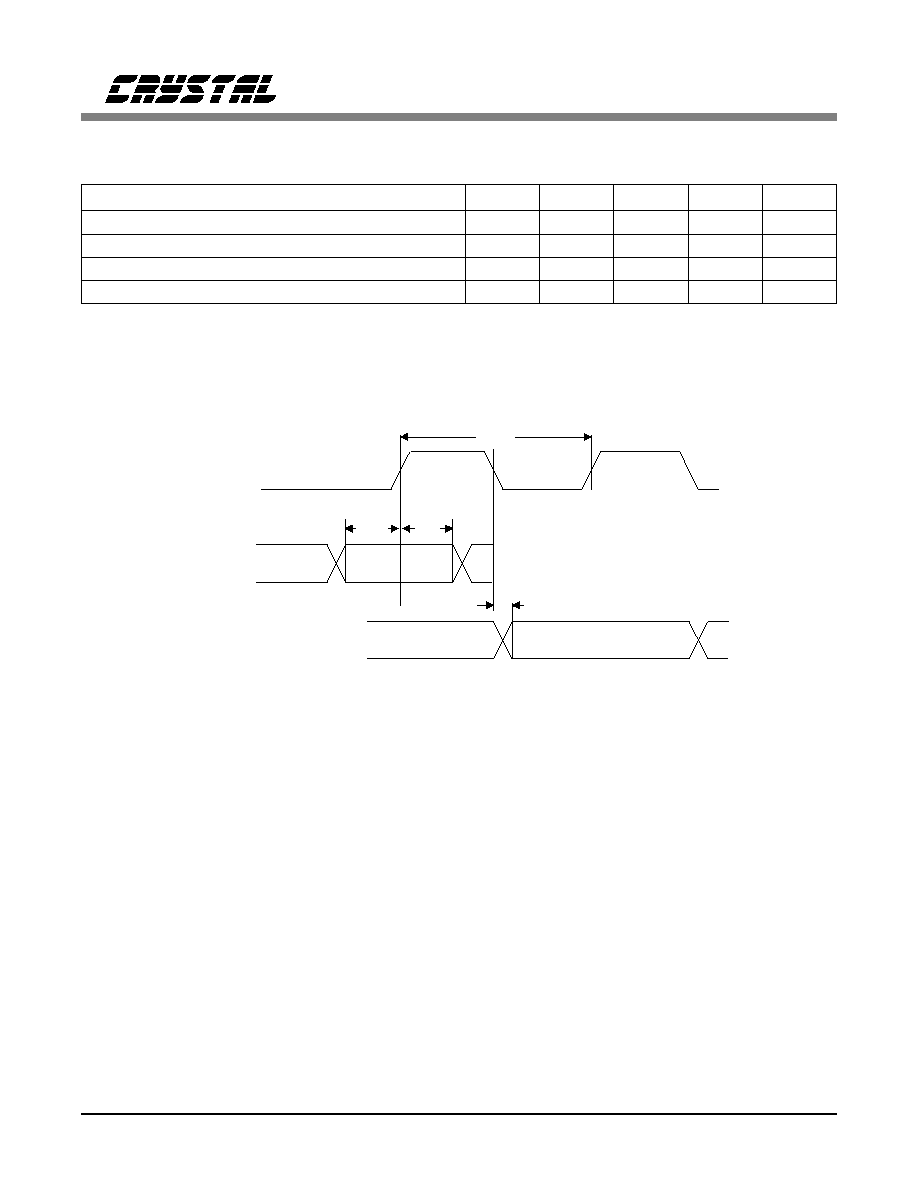
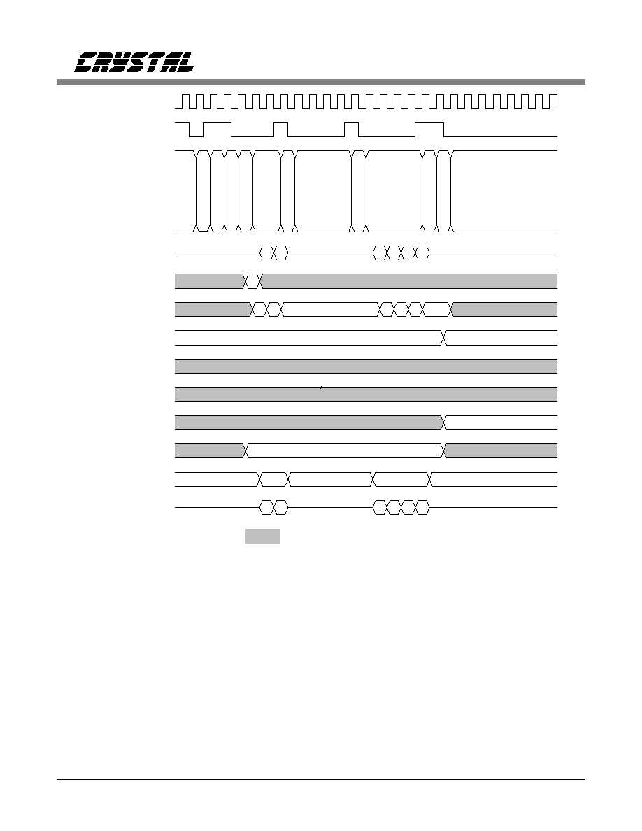
Figure 1. Signal Rise and Fall Characteristics
RCLK
(CLKE = 1)
t
pwl1
t
pwh1
RCLK
(CLKE =0)
RPOS
RNEG
RDATA
BPV
h1
t
su1
t
tpw1
Figure 2. Recovered Clock and Data Switching Characteristics
TCLK
TPOS
TNEG
TDATA
t
su2
t
h2
t
pwh2
t
pw2
Figure 3. Transmit Clock and Data Switching Characteristics
CS61583
DS172PP5
7
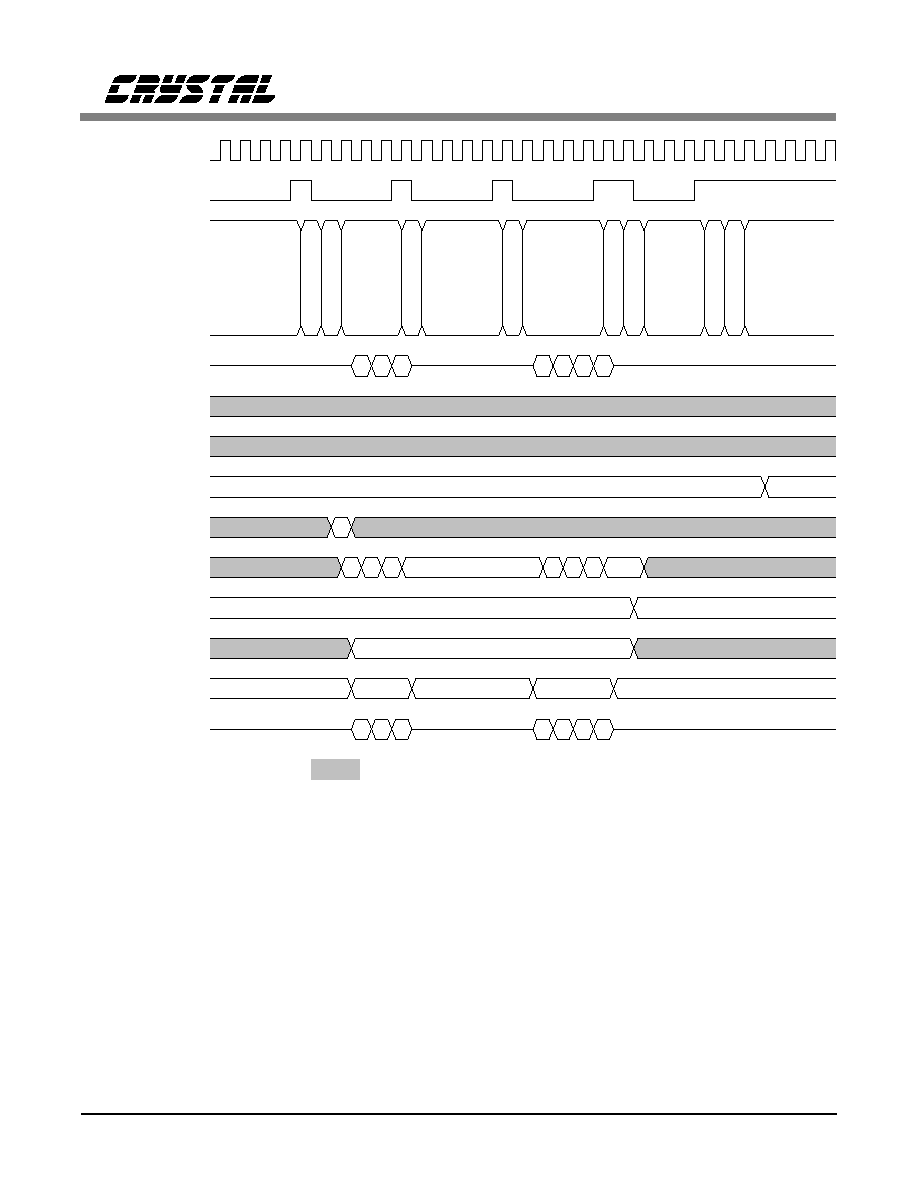
J-TCK
J-TMS
J-TDI
J-TDO
t cyc
t dv
t su
t h
Figure 4. JAG Switching Characteristics
SWITCHING CHARACTERISTICS - JTAG
(T
A
= - 40
∞
to 85
∞
C;
TV+, RV+ = nominal
±
0.3V; Inputs: Logic 0 = 0V, Logic 1 = RV+) (See Figure 4)
Parameter
Symbol
Min
Typ
Max
Units
Cycle Time
t
cyc
200
-
-
ns
J-TMS/J-TDI to J-TCK rising setup time
t
su
50
-
-
ns
J-TCK rising to J-TMS/J-TDI hold time
t
h
50
-
-
ns
J-TCK falling to J-TDO valid
t
dv
-
-
50
ns
CS61583
8
DS172PP5

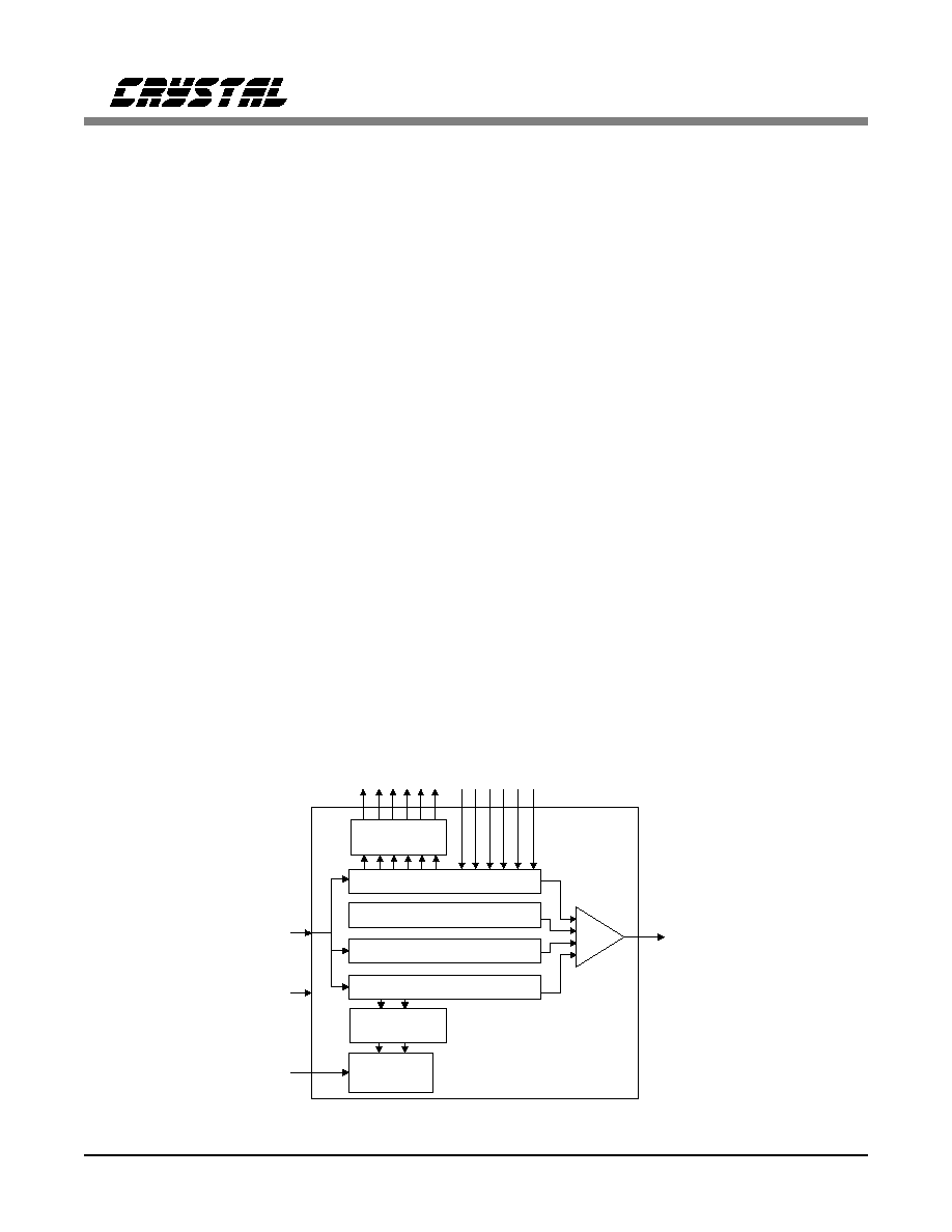
OVERVIEW
The CS61583 is a dual line interface for T1/E1
applications, designed for high-volume cards
where low power and high density are required.
One board design can support all T1/E1 short-
haul modes by only changing component values
in the receive and transmit paths (if REFCLK
and TCLK are externally tied together). Figure 5
illustrates applications of the CS61583 in various
environments.
All control of the device is achieved via external
pins, eliminating the need for microprocessor
support. The following pin control options are
available on a per channel basis: line length se-
lection, coder mode, jitter attenuator location,
transmit all ones, local loopback, and remote
loopback.
The line driver generates waveforms compatible
with E1 (CCITT G.703), T1 short haul (DSX-1),
and T1 FCC Part 68 Option A (DS1). A single
transformer turns ratio is used for all waveform
types. The driver internally matches the imped-
ance of the load, providing excellent return loss
to insure superior T1/E1 pulse quality. An addi-
A SYNCHR O N OU S MU X APPLICAT IO N
(i.e., VT1.5 card for SO NET or SD H m ux)
SYN CHR O N OU S A PPLICATIO N
(Including 62411 system s w ith m ultiple T1 lines)
T T IP
T P O S
T N E G
R N E G
TR IN G
R P O S
R R IN G
R T IP
C S 6218 0 B
FR A M E R
JIT TE R
A T TE N U A T O R
C S 6 1 5 8 3
LIN E D R IV ER
L IN E R E C E IV E R
R E C E IVE
C IR C U IT R Y
T R A N S M IT
C IR C U IT R Y
R C L K
TC LK
R E F C L K
T T IP
TD A TA
R D A TA
T R IN G
L IN E D R IV E R
A M I
B 8ZS ,
H D B 3 ,
C O D E R
R R IN G
R TIP
M U X
C S 6 1 5 8 3
JIT T E R
A T T E N U A T O R
R E F C L K
R C LK
TC L K
(ga pp ed )
T T IP
T P O S
T N E G
R N EG
T R IN G
R P O S
R R IN G
R T IP
C S 62 1 8 0 B
FR A M E R
JIT TE R
A T TE N U A T O R
C S 6 1 5 8 3
LIN E D R IV ER
LIN E R E C E IV ER
R C L K
T C LK
R E F C LK
A IS
D E T E C T
L IN E R E C E IV E R
R E C E IVE
C IR C U IT R Y
T R A N S M IT
C IR C U IT R Y
R E C E IVE
C IR C U IT R Y
T R A N S M IT
C IR C U IT R Y
L O O P T IM E D AP P L IC A TIO N
Figure 5. Examples of CS61583 Applications
CS61583
DS172PP5
9

tional benefit of the internal impedance matching
is a 50 percent reduction in power consumption
compared to implementing return loss using ex-
ternal resistors that causes the transmitter to
drive the equivalent of two line loads.
The line receiver contains all the necessary clock
and data recovery circuits.
The jitter attenuator meets AT&T 62411 require-
ments when using a 1X or 8X reference clock
supplied by either a crystal oscillator or external
reference at the REFCLK input pin.
AT&T 62411 Customer Premises Application
The AT&T 62411 specification applies to the T1
interface between the customer premises and the
carrier, and must be implemented by the cus-
tomer premises equipment in order to connect to
the AT&T network.
In 62411 applications, the management of jitter
is a very important design consideration. Typi-
cally, the jitter attenuator is placed in the receive
path of the CS61583 to reduce the jitter input to
the system synchronizer. The jitter attenuated re-
covered clock is used as the input to the transmit
clock to implement a loop-timed system. A Stra-
tum 4 (
±32
ppm) quality clock or better should
be input to REFCLK. Note that any jitter present
on the reference clock will not be filtered by the
jitter attenuator.
Asynchronous Multiplexer Application
Asynchronous multiplexers accept multiple
T1/E1 lines (which are asynchronous to each
other), and combine them into a higher speed
transmission rate (e.g. M13 muxes and SONET
muxes). In these systems, the jitter attenuator is
placed in the transmit path of the CS61583 to
remove the gapped clock jitter input by the mul-
tiplexer to TCLK. Because the transmit clock is
jittered, the reference clock to the CS61583 is
provided by an external source operating at 1X
or 8X the data rate. Because T1/E1 framers are
not usually required in asynchronous multiplex-
e rs, the B8 ZS/AMI/HDB3 coders in the
CS61583 are activated to provide data interfaces
on TDATA and RDATA.
Synchronous Application
A typical example of a synchronous application
is a T1 card in a central office switch or a 0/1
digital cross-connect system. These systems
place the jitter attenuator in the receive path to
reduce the jitter presented to the system. A Stra-
tum 3 or better system clock is input to the
CS61583 transmit and reference clocks.
TRANSMITTER
The transmitter accepts data from a T1 or E1
system and outputs pulses of appropriate shape
to the line. The transmit clock (TCLK) and
transmit data (TPOS & TNEG, or TDATA) are
supplied synchronously. Data is sampled on the
falling edge of the TCLK input.
The configuration pins CON[2:0] control trans-
m i t t e d p u l s e s h a p e s , t r a n s m i t t e r so u r ce
impedance, and receiver slicing level as shown in
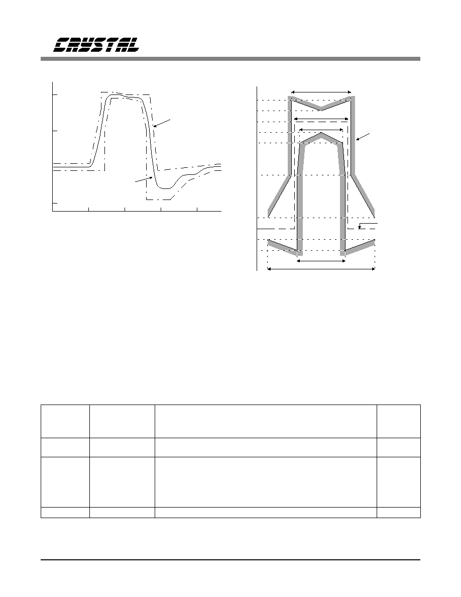
Table 1. Typical output pulses are shown in Figures
6 and 7. These pulse shapes are fully pre-defined
by circuitry in the CS61583, and are fully compli-
ant with appropriate standards when used with our
application guidelines in standard installations.
Both channels must be operated at the same line rate
(both T1 or both E1).
Note that the pulse width for Part 68 Option A
(324 ns) is narrower than the optimal pulse
width for DSX-1 (350 ns). The CS61583 auto-
matically adjusts the pulse width based on the
configuration selection.
The transmitter impedance changes with the line
length options in order to match the load imped-
ance (75
for E1 coax, 100
for T1, 120
for
E1 shielded twisted pair), providing a minimum
of 14 dB return loss for T1 and E1 frequencies
CS61583
10
DS172PP5
during the transmission of both marks and
spaces. This improves signal quality by minimiz-
ing reflections from the transmitter. Impedance
matching also reduces load power consumption
by a factor of two when compared to the return
loss achieved by using external resistors.
The CS61583 driver will automatically detect an
inactive TLCK input (i.e., no valid data is being
clocked to the driver). When this condition is de-
tected, the driver is forced low (except during
remote loopback) to output spaces and prevent
TTIP and TRING from entering a constant trans-
mit-mark state.
When any transmit configuration established by
CON[2:0], TAOS, or LLOOP changed states, the
transmitter stabilizes within 22 TCLK bit peri-
ods. The transmitter takes longer to stabilize
when RLOOP1 or RLOOP2 is selected because
the timing circuitry must adjust to the new fre-
quency from RCLK.
When the transmitter transformer secondaries are
shorted through a 0.5 ohm resistor, the transmit-
500
1.0
0.5
0
-0.5
0
250
750
1000
NORMALIZED
AMPLITUDE
CS61583
OUTPUT
PULSE SHAPE
TIME (nanoseconds)
ANSI T1.102
SPECIFICATION
Figure 6. Typical Pulse Shape at DSX-1 Cross Connect
269 ns
244 ns
194 ns
219 ns
488 ns
Nominal Pulse
0
10
50
80
90
100
110
120
-10
-20
Percent of
nominal
peak
voltage
G.703
Specification
Figure 7. Pulse Mask at the 2048 kbps Interface
C
O
N
2
C
O
N
1
C
O
N
0
Transmit Pulse
Width at 50%
Amplitude
Transmit Pulse Shape
Receiver
Slicing
Level
0
0
0
0
0
1
244 ns (50%)
244 ns (50%)
E1: square, 2.37 Volts into 75
E1: square, 3.00 Volts into 120
50%
50%
0
1
0
350 ns (54%)
DSX-1: 0-133 ft. / or DS1 FCC Part 68 Option A with undershoot
65%
0
1
1
350 ns (54%)
DSX-1: 133-266 ft.
65%
1
0
0
350 ns (54%)
DSX-1: 266-399 ft.
65%
1
0
1
350 ns (54%)
DSX-1: 399-533 ft.
65%
1
1
0
350 ns (54%)
DSX-1: 533-655 ft.
65%
1
1
1
324 ns (50%)
DS1: FCC Part 68 Option A (0 dB)
65%
Table 1. Configuration Selection
CS61583
DS172PP5
11

ter will output a maximum of 50 mA-rms, as re-
quired by European specification BS6450.
RECEIVER
The receiver extracts data and clock from the
T1/E1 signal on the line interface and outputs
clock and synchronized data to the system. The
signal is detected differentially across the receive
transformer and can be recovered over the entire
range of short haul cable lengths. The transmit
and receive transfomer specifications are identical
and are presented in the Applications section.
As shown in Table 1, the receiver slicing level is
set at 65% for DS1/DSX-1 short-haul and at
50% for all other applications.
The clock recovery circuit is a second-order
phase locked loop that can tolerate up to 0.4 UI
of jitter from 10 kHz to 100 kHz without gener-
ating errors (Figure 8). The clock and data
recovery circuit is tolerant of long strings of con-
secutive zeros and will successfully recover a
1-in-175 jitter-free line input signal.
Re co vered data at RPOS and RNEG (or
RDATA) is stable and may be sampled using the
recovered clock RCLK. The CLKE input deter-
mines the clock polarity for which output data is
stable and valid as shown in Table 2. When
CLKE is low, RPOS and RNEG (or RDATA) are
valid on the rising edge of RCLK. When CLKE
is high, RPOS and RNEG (or RDATA) are valid
on the falling edge of RCLK.
CLKE
DATA
CLOCK
Clock Edge
for Valid Data
LOW
RPOS, RNEG
or RDATA
RCLK
RCLK
Rising
Rising
HIGH
RPOS, RNEG
or RDATA
RCLK
RCLK
Falling
Falling
Table 2. Recovered Data/Clock Options
JITTER ATTENUATOR
The jitter attenuator can be switched into either
the receive or transmit paths. Alternatively, it can
also be removed from both paths to reduce the
propagation delay.
The location of the attenuators for both channels
is controlled by the ATTEN0 and ATTEN1 pins.
Table 3 shows how these pins are decoded.
The attenuator consists of a 64-bit FIFO, a nar-
row-band monolithic PLL, and control logic.
Signal jitter is absorbed in the FIFO which is de-
signed to neither overflow nor underflow. If
overflow or underflow is imminent, the jitter
transfer function is altered to insure that no bit-
errors occur. Under this condition, jitter gain
may occur and jitter should be attenuated exter-
nally in a frame buffer. The jitter attenuator will
typically tolerate 43 UIs before the overflow/un-
d er f l o w m ec h a n i s m o c cu r s . I f t h e j it ter
attenuator has not had time to "lock" to the aver-
10
1k
10k
1
100
100k
700
.1
1
10
100
.4
28
300
300
PEAK-TO-PEAK
JITTER
(unit intervals)
JITTER FREQUENCY (Hz)
CS61583
Performance
138
AT&T 62411
(1990 Version)
Figure 8. Minimum Input Jitter Tolerance of Receiver
(Clock Recovery Circuit and Jitter Attenuator)
ATTEN1
ATTEN0
Location of
Jitter Attenuator
0
0
Receiver
0
1
Disabled
1
0
Transmitter
1
1
Reserved
Table 3. Jitter Attenuation Control
CS61583
12
DS172PP5

age incoming frequency (e.g. following a device
reset) the attenuator will tolerate a minimum of
22 UIs before the overflow/underflow mecha-
nism occurs.
For T1/E1 line cards used in high-speed muti-
plexers (e.g., SONET and SDH), the jitter
attenuator is typically used in the transmit path.
The attenuator can accept a transmit clock with
gaps
28 UIs and a transmit clock burst rate of
8 MHz.
When the jitter attenuator is in the receive path and
loss of signal occurs, the frequency of the last re-
covered signal is held. When the jitter attenuator is
not in the receive path, the last recovered frequency
is not held and the output frequency becomes the
frequency of the reference clock.
A typical jitter attenuation curve is shown in Fig-
ure 9.
REFERENCE CLOCK
The CS61583 requires a reference clock with a
minimum accuracy of
±100
ppm for T1 and E1
applications. This clock can be either a 1X clock
(i.e., 1.544 MHz or 2.048 MHz), or can be a 8X
clock (i.e., 12.352 MHz or 16.384 MHz) as se-
lected by the 1XCLK pin. In systems with a
jittered transmit clock, the reference clock
should not be tied to the transmit clock and a
separate external oscillator should drive the ref-
erence clock input. Any jitter present on the
reference clock will not be filtered by the jitter
attenuator.
POWER-UP RESET
On power-up, the device is held in a static state
until the power supply achieves approximately
60% of the power supply voltage. When this
threshold is crossed, the device waits another 10
ms to allow the power supply to reach operating
voltage and then calibrates the transmit and re-
ceive circuitry. This initial calibration takes less
than 20 ms but can occur only if REFCLK and
TCLK are present. The power-up reset performs
the same functions as the RESET pin.
LINE CONTROL AND MONITORING
Line control and monitoring of the CS61583 is
achieved using the control pins. The controls and
indications available on the CS61583 are de-
tailed below.
Line Code Encoder/Decoder
Coding may be transparent, AMI, B8ZS, or
HDB3 and is selected using the CODER1,
CODER2, AMI1, and AMI2 pins. In the coder
mode, AMI, B8ZS, and HDB3 line codes are
available. The input data to the encoder is on
TDATA and the output data from the decoder is
in NRZ format on RDATA. See Table 4.
CODER[2:1]=0
CODER[2:1]=1
Transparent Mode
Enabled
and
AMI[2:1] Pin(s)
Disabled
AMI[2:1]=0
B8ZS/HDB3
Encoder/Decoder
Enabled
AMI[2:1]=1
AMI
Encoder/Decoder
Enabled
Table 4. Coder Mode Options
A
t
t
e
n
uat
i
on i
n
dB
Frequency in Hz
0
10
20
30
40
50
60
1
10
100
1 k
10 k
b) Maximum
Attenuation
Limit
62411 (1990 Version)
Requirements
a) Minimum Attenuation Limit
CS61583 Performance
Figure 9. Typical Jitter Transfer Function
CS61583
DS172PP5
13

Alarm Indication Signal
In coder mode, the TNEG pin becomes the
alarm indication signal (AIS) output controlled
by the receiver. The receiver detects the AIS
condition on observation of 99.9% ones density
in a 5.3 ms period (< 9 zeros in 8192 bits) and
sets the AIS pin high. The AIS condition is ex-
ited when
9 zeros are detected in 8192 bits.
Bipolar Violation Detection
In coder mode, the RNEG pin becomes the bipo-
lar violation (BPV) strobe output controlled by
the receiver. The BPV pin goes high for one
RCLK period when a bipolar violation is de-
tected in the received signal. Note that B8ZS or
HDB3 zero substitutions are not flagged as bipo-
lar violations when the decoder is enabled.
Loss of Signal
The loss of signal (LOS) indication is detected
by the receiver and reported when the LOS pin
is high. Loss of signal is indicated when 175
±
15
consecutive zeros are received. The LOS condi-
t i o n i s e x i ted accordi ng to t h e ANSI
T1.231-1993 criteria that requires 12.5% ones
density over 175
±
75 bit periods with no more
than 100 consecutive zeros. Note that bit errors
may occur at RPOS and RNEG (or RDATA)
prior to the LOS indication if the analog input
level falls below the receiver sensitivity.
The LOS pin is set high when the device is reset
or in powered up and returns low when data is
recovered by the receiver.
Transmit All Ones
Transmit all ones is selected by setting the
TAOS pin high. Selecting TAOS causes continu-
ous ones to be transmitted to the line interface
on TTIP and TRING at the frequency of
REFCLK. In this mode, the transmit data inputs
TPOS and TNEG (or TDATA) are ignored. A
TAOS overrides the data transmitted to the line
interface during local and remote loopbacks.
Local Loopback
A local loopback is selected by setting the
LLOOP pin high. Selecting LLOOP causes the
TCLK, TPOS, and TNEG (or TDATA) inputs to
be looped back through the jitter attenuator (if
enabled) to the RCLK, RPOS, and RNEG (or
RDATA) outputs. Data received at the line inter-
face is ignored, but data at TPOS and TNEG (or
TDATA) continues to be transmitted to the line
interface at TTIP and TRING.
A TAOS request overrides the data transmitted to
the line interface during local loopback. Note
that simultaneous selection of local and remote
loopback modes is not valid.
Remote Loopback
A remote loopback is selected by setting the
RLOOP pin high. Selecting RLOOP causes the
data received from the line interface at RTIP and
RRING to be looped back through the jitter at-
tenuator (if enabled) and retransmitted on TTIP
and TRING. Data transmitted at TPOS and
TNEG (or TDATA) is ignored, but data recov-
ered from RTIP and RRING continues to be
transmitted on RPOS and RNEG (or RDATA).
Remote loopback is functional if TCLK is ab-
sent. A TAOS request overrides the data
transmitted to the line interface during a remote
loopback. Note that simultaneous selection of lo-
cal and remote loopback modes is not valid.
Reset Pin
The CS61583 is continuously calibrated during
operation to insure the performance of the device
over power supply and temperature. The con-
tinuous calibration function eliminates the need
to reset the line interface during operation.
A device reset may be selected by setting the
RESET pin high for a minimum of 200 ns. The
reset function initiates on the falling edge of RE-
SET and takes less than 20 ms to complete. The
control logic is initialized and the transmit and
CS61583
14
DS172PP5
receive circuitry is calibrated if REFCLK and
TCLK are present.
JTAG BOUNDARY SCAN
Board testing is supported through JTAG bound-
ary scan. Using boundary scan, the integrity of
the digital paths between devices on a circuit
board can be verified. This verification is sup-
ported by the ability to externally set the signals
on the digital output pins of the CS61583, and to
externally read the signals present on the input
pins of the CS61583. Additionally, the manufac-
turer ID, part number and revision of the
CS61583 can be read during board test using
JTAG boundary scan.
As shown in Figure 10, the JTAG hardware con-
sists of data and instruction registers plus a Test
Access Port (TAP) controller. Control of the TAP
is achieved through signals applied to the Test
Mode Select (J-TMS) and Test Clock ( J-TCK)
input pins. Data is shifted into the registers via
the Test Data Input (J-TDI) pin, and shifted out
of the registers via the Test Data Output (J-TDO)
pin. Both J-TDI and J-TDO are clocked at a rate
determined by J-TCK. The Instruction register
defines which data register is accessed in the
shift operation. Note that if J-TDI is floating,
an internal pull-up resistor forces the pin high.
JTAG Data Registers (DR)
The test data registers are the Boundary-Scan
Register (BSR), the Device Identification Regis-
ter (DIR), and the Bypass Register (BR).
Boundary Scan Register: The BSR is connected
in parallel to all the digital I/O pins, and pro-
vides the mechanism for applying/reading test
patterns to/from the board traces. The BSR is 67
bits long and is initialized and read using the in-
struction SAMPLE/PRELOAD. The bit ordering
for the BSR is the same as the top-view package
pin out, beginning with the LOS1 pin and mov-
ing counter-clockwise to end with the CODER1
pin as shown in Table 5. Note that the analog,
oscillator, power, ground, CLKE, and ATTEN0
pins are not included as part of the boundary-
scan register.
The input pins require one bit in the BSR and
only one J-TCK cycle is required to load test
data for each input pin.
The output pins have two bits in the BSR to de-
fine output high, output low, or high impedance.
MUX
J-TDI
J-TCK
J-TMS
J-TDO
JTAG Block
Boundary Scan Data Register
Digital output pins
Digital input pins
parallel latched
output
TAP
Controller
Instruction (shift) Register
Bypass Data Register
Device ID Data Register
parallel latched
output
Figure 10. Block Diagram of JTAG Circuitry
CS61583
DS172PP5
15
The first bit (shifted in first) selects between an
output-enabled state (bit set to 1) or high-imped-
ance state (bit set to 0). The second bit shifted in
contains the test data that may be output on the
pin. Therefore, two J-TCK cycles are required to
load test data for each output pin.
The bi-directional pins have three bits in the
BSR to define input, output high, output low, or
high impedance. The first bit shifted into the
BSR configures the output driver as high-imped-
ance (bit set to 0) or active (bit set to 1). The
second bit shifted into the BSR sets the output
value when the first bit is 1. The third bit cap-
tures the value of the pin. This pin may have its
value set externally as an input (if the first bit is
0) or set internally as an output (if the first bit is
1). To configure a pad as an input, the J-TDI
pattern is 0X0. To configure a pad as an output,
the J-TDI pattern is 1X1. Therefore, three J-TCK
cycles are required to load test data for each bi-
directional pin.
Device Identification Register: The DIR provides
the manufacturer, part number, and version of the
CS61583. This information can be used to verify
that the proper version or revision number has
been used in the system under test. The DIR is 32
bits long and is partitioned as shown in figure 11.
Data from the DIR is shifted out to J-TDO LSB
first.
Bypass Register: The Bypass register consists of
a single bit, and provides a serial path between
J-TDI and J-TDO, bypassing the BSR. This al-
lows bypassing specific devices during certain
board-level tests. This also reduces test access
times by reducing the total number of shifts re-
quired from J-TDI to J-TDO.
BIT #(s)
FUNCTION
Total Bits
31-28
Version number
4
27-12
Part Number
16
11-1
Manufacturer Number
11
0
Constant Logic '1'
1
Figure 11. Device Identification Register
MSB
LSB
31
28 27
12 11
1 0
0 0 0 0 0 0 0 0 0 0 0 0 0 0 0 0 0 0 1 1 0 0 0 0 1 1 0 0 1 0 0 1
(4 bits)
(16 bits)
(11 bits)
BSR bits
Pin Name
Pad Type
0-2
LOS1
bi-directional
2
3-5
TNEG1/AIS1
bi-directional
6
TPOS1/TDATA1
input
7
TCLK1
input
8-9
RNEG1/BPV1
output
10-11
RPOS1/RDATA1
output
12-13
RCLK1
output
14-16
ATTEN1
bi-directional
1
17-19
RLOOP1
bi-directional
1
20
LLOOP1
input
21-23
LLOOP2
bi-directional
1
24-26
TAOS1
bi-directional
1
27-29
TAOS2
bi-directional
1
30-32
CON01
bi-directional
1
33-35
CON02
bi-directional
1
36-38
CON11
bi-directional
1
39-41
CON12
bi-directional
1
42-44
CON21
bi-directional
1
45
CON22
input
46-48
AMI1
bi-directional
1
49-50
RCLK2
output
51-52
RPOS2/RDATA2
output
53-54
RNEG2/BPV2
output
55
TCLK2
input
56
TPOS2/TDATA2
input
57-59
TNEG2/AIS2
bi-directional
60-62
LOS2
bi-directional
2
63
AMI2
input
64
CODER2
input
65
RLOOP2
input
66
CODER1
input
1. Configure pad as an input.
2. Configure pad as an output.
Table 5. Boundary Scan Register
CS61583
16
DS172PP5

JTAG Instructions and Instruction Register (IR)
The instruction register (2 bits) allows the in-
struction to be shifted into the JTAG circuit. The
instruction selects the test to be performed or the
data register to be accessed or both. The valid
instructions are shifted in LSB first and are listed
below:
IR CODE
INSTRUCTION
00
EXTEST
01
SAMPLE/PRELOAD
10
IDCODE
11
BYPASS
EXTEST Instruction: The EXTEST instruction
allows testing of off-chip circuitry and board-
level interconnect. EXTEST connects the BSR to
the J-TDI and J-TDO pins. The normal path be-
tween the CS61583 logic and I/O pins is broken.
The signals on the output pins are loaded from
the BSR and the signals on the input pins are
loaded into the BSR.
SAMPLE/PRELOAD Instruction: The SAM-
PLE/PRELOAD instructions allows scanning of
the boundary-scan register without interfering
with the operation of the CS61583. This instruc-
tion connects the BSR to the J-TDI and J-TDO
pins. The normal path between the CS61583
logic and its I/O pins is maintained. The signals
on the I/O pins are loaded into the BSR. Addi-
tionally, this instruction can be used to latch
values into the digital output pins.
IDCODE Instruction: The IDCODE instruction
connects the device identification register to the
J-TDO pin. The IDCODE instruction is forced
into the instruction register during the Test-
L o g i c- R ese t co nt r o l l e r st a t e. The defaul t
instruction is IDCODE after a device reset.
BYPASS Instruction: The BYPASS instruction
connects the minimum length bypass register be-
tween the J-TDI and J-TDO pins and allows data
to be shifted in the Shift-DR controller state.
Internal Testing Considerations
Note that the INTEST instruction is not sup-
ported because of the difficulty in performing
significant internal tests using JTAG.
The one test that could be easily performed us-
ing an arbitrary clock rate on TCLK and
REFCLK is a local loopback with jitter attenu-
ator disabled. However, this test provides limited
fault coverage and is only useful in determining
if the device had been catastrophically destroyed.
Alternatively, catastrophic destruction of the de-
vice and/or surrounding board traces can be
detected using EXTEST. Therefore, the INTEST
instruction provides limited testing capability
and was not included in the CS61583.
JTAG TAP Controller
Figure 12 shows the state diagram for the TAP
state machine. A description of each state fol-
lows. Note that the figure contains two main
branches to access either the data or instruction
registers. The value shown next to each state
transition in this figure is the value present at
J-TMS at each rising edge of J-TCK.
Test-Logic-Reset State
In this state, the test logic is disabled to continue
normal operation of the device. During initiali-
zation, the CS61583 initializes the instruction
register with the IDCODE instruction.
Regardless of the original state of the controller,
the controller enters the Test-Logic-Reset state
when the J-TMS input is held high for at least
five rising edges of J-TCK. The controller re-
mains in this state while J-TMS is high. The
CS61583 processor automatically enters this
state at power-up.
Run-Test/Idle State
This is a controller state between scan opera-
tions. Once in this state, the controller remains
in the state as long as J-TMS is held low. The
CS61583
DS172PP5
17

instruction register and all test data registers re-
tain their previous state. When J-TMS is high
and a rising edge is applied to J-TCK, the con-
troller moves to the Select-DR state.
Select-DR-Scan State
This is a temporary controller state. The test
data register selected by the current instruction
retains its previous state. If J-TMS is held low
and a rising edge is applied to J-TCK when in
this state, the controller moves into the Capture-
DR state and a scan sequence for the selected
test data register is initiated. If J-TMS is held
high and a rising edge applied to J-TCK, the
controller moves to the Select-IR-Scan state.
The instruction does not change in this state.
Capture-DR State
In this state, the Boundary Scan Register cap-
tures input pin data if the current instruction is
EXTEST or SAMPLE/PRELOAD. The other
test data registers, which do not have parallel in-
put, are not changed.
The instruction does not change in this state.
When the TAP controller is in this state and a
rising edge is applied to J-TCK, the controller
enters the Exit1-DR state if J-TMS is high or the
Shift-DR state if J-TMS is low.
Shift-DR State
In this controller state, the test data register con-
nected between J-TDI and J-TDO as a result of
the current instruction shifts data on stage to-
ward its serial output on each rising edge of
J-TCK.
The instruction does not change in this state.
When the TAP controller is in this state and a
rising edge is applied to J-TCK, the controller
enters the Exit1-DR state if J-TMS is high or re-
mains in the Shift-DR state if J-TMS is low.
Exit1-DR State
This is a temporary state. While in this state, if
J-TMS is held high, a rising edge applied to J-
T C K c au s es t h e c o n t rol ler to enter the
Update-DR state, which terminates the scanning
process. If J-TMS is held low and a rising edge
is applied to J-TCK, the controller enters the
Pause-DR state.
Test-Logic-Reset
Run-Test/Idle
Select-DR-Scan
Capture-DR
Shift-DR
Exit1-DR
Pause-DR
Exit2-DR
Update-DR
Select-IR-Scan
Capture-IR
Shift-IR
Exit1-IR
Pause-IR
Exit2-IR
Update-IR
1
0
0
1
1
0
1
0
1
1
0
1
0
0
1
0
1
0
0
1
1
0
1
1
0
1
0
0
1
0
1
0
Figure 12. TAP Controller State Diagram
CS61583
18
DS172PP5

The test data register selected by the current in-
struction retains its previous value during this
state. The instruction does not change in this
state.
Pause-DR State
The pause state allows the test controller to tem-
porarily halt the shifting of data through the test
data register in the serial path between J-TDI and
J-TDO. For example, this state could be used to
allow the tester to reload its pin memory from
disk during application of a long test sequence.
The test data register selected by the current in-
struction retains its previous value during this
state. The instruction does not change in this
state.
The controller remains in this state as long as
J-TMS is low. When J-TMS goes high and a
rising edge is applied to J-TCK, the controller
moves to the Exit2-DR state.
Exit2-DR State
This is a temporary state. While in this state, if
J-TMS is held high, a rising edge applied to J-
T C K c au s es t h e c o n t rol ler to enter the
Update-DR state, which terminates the scanning
process. If J-TMS is held low and a rising edge
is applied to J-TCK, the controller enters the
Shift-DR state.
The test data register selected by the current in-
struction retains its previous value during this
state. The instruction does not change in this
state.
Update-DR State
The Boundary Scan Register is provided with a
latched parallel output to prevent changes while
data is shifted in response to the EXTEST and
SAMPLE/PRELOAD instructions. When the
TAP controller is in this state and the Boundary
Scan Register is selected, data is latched into the
parallel output of this register from the shift-reg-
ister path on the falling edge of J-TCK. The
data held at the latched parallel output changes
only in this state.
All shift-register stages in the test data register
selected by the current instruction retains their
previous value during this state. The instructions
does not change in this state.
Select-IR-Scan State
This is a temporary controller state. The test
data register selected by the current instruction
retains its previous state. If J-TMS is held low
and a rising edge is applied to J-TCK when in
this state, the controller moves into the Capture-
IR state, and a scan sequence for the instruction
register is initiated. If J-TMS is held high and a
rising edge is applied to J-TCK, the controller
moves to the Test-Logic-Reset state. The in-
struction does not change in this state.
Capture-IR State
In this controller state, the shift register con-
tained in the instruction register loads a fixed
value of "01" on the rising edge of J-TCK. This
supports fault-isolation of the board-level serial
test data path.
Data registers selected by the current instruction
retain their value during this state. The instruc-
tions does not change in this state.
When the controller is in this state and a rising
edge is applied to J-TCK, the controller enters
the Exit1-IR state if J-TMS is held high, or the
Shift-IR state if J-TMS is held low.
Shift-IR State
In this state, the shift register contained in the
instruction register is connected between J-TDI
and J-TDO and shifts data one stage towards its
serial output on each rising edge of J-TCK.
CS61583
DS172PP5
19

The test data register selected by the current in-
struction retains its previous value during this
state. The instruction does not change in this
state.
When the controller is in this state and a rising
edge is applied to J-TCK, the controller enters
the Exit1-IR state if J-TMS is held high, or re-
mains in the Shift-IR state if J-TMS is held low.
Exit1-IR State
This is a temporary state. While in this state, if
J-TMS is held high, a rising edge applied to J-
TCK causes the controller to enter the Update-IR
state, which terminates the scanning process. If
J-TMS is held low and a rising edge is applied
to J-TCK, the controller enters the Pause-IR
state.
The test data register selected by the current in-
struction retains its previous value during this state.
The instruction does not change in this state.
Pause-IR State
The pause state allows the test controller to tem-
porarily halt the shifting of data through the
instruction register.
The test data register selected by the current in-
struction retains its previous value during this
state. The instruction does not change in this
state.
The controller remains in this state as long as
J-TMS is low. When J-TMS goes high and a
rising edge is applied to J-TCK, the controller
moves to the Exit2-IR state.
Exit2-IR State
This is a temporary state. While in this state, if
J-TMS is held high, a rising edge applied to J-
TCK causes the controller to enter the Update-IR
state, which terminates the scanning process. If
J-TMS is held low and a rising edge is applied
to J-TCK, the controller enters the Shift-IR state.
The test data register selected by the current in-
struction retains its previous value during this
state. The instruction does not change in this
state.
Update-IR State
The instruction shifted into the instruction regis-
ter is latched into the parallel output from the
shift-register path on the falling edge of J-TCK.
When the new instruction has been latched, it
becomes the current instruction.
Test data registers selected by the current in-
struction retain their previous value.
JTAG Application Examples
Figures 13 and 14 illustrate examples of updat-
ing the instruction and data registers during
JTAG operation.
CS61583
20
DS172PP5
TCK
TMS
Controller state
TDI
IR shift-register
Parallel output of IR
Parallel Input to TDR
TDR shift-register
Parallel output of TDR
Register selected
TDO enable
TDO
Act
IDCODE
New Instruction
Old data
Instruction register
Inactive
Active
Inactive
Inactive
= Don't care or undefined
Parallel Input to IR
T
est-
L
o
g
i
c
-R
eset
R
un-T
est/
I
d
l
e
S
e
l
ect
-DR-S
can
S
e
le
ct-I
R-Sc
an
Cap
t
ure-I
R
P
o
u
se-I
R
Ex
i
t
2-
IR
S
h
i
f
t-
IR
Ex
i
t
1-
IR
Upd
a
t
e
-I
R
R
un-T
est/
I
d
l
e
Ex
i
t
1-
IR
S
h
i
f
t-
IR
Figure 13. JTAG Instruction Register Update
CS61583
DS172PP5
21
TCK
TMS
Controller state
TDI
Parallel Input to IR
IR shift-register
Parallel output of IR
Parallel Input to TDR
TDR shift-register
Register Selected
TDO enable
TDO
= Don't care or undefined
Parallel output of TDR
T
est
-Lo
g
i
c
-Re
set
Run
-
T
est
/I
dl
e
S
e
l
e
ct-
D
R
-
Sc
an
S
e
l
e
ct-
D
R
-
Sc
an
Cap
t
ure-D
R
P
ouse-
DR
Ex
i
t
2
-
DR
Shi
f
t
-
D
R
Upd
a
t
e
-D
R
Run
-
T
est
/I
dl
e
Ex
i
t
1
-
DR
Shi
f
t
-
D
R
Ex
i
t
1
-
DR
Se
l
e
ct
-
I
R
-
Sc
an
IDCODE
Instruction
Old data
Test data register
New data
Inactive
Active
Inactive
Inactive
Active
Figure 14. JTAG Data Register Update
CS61583
22
DS172PP5
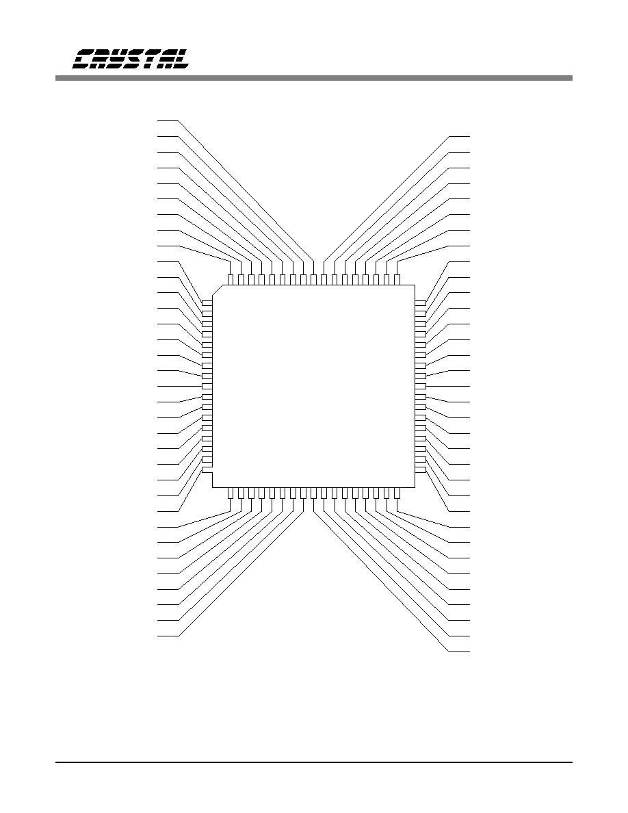
PIN DESCRIPTIONS
11
13
15
17
19
21
23
25
1
3
5
7
9
67
65
63
61
35
33
31
29
27
37 39 41
43
45
47
49
51
53
55
57
59
CS61583
68-Pin PLCC
Top View
DGND1
CON01
TAOS2
TAOS1
LLOOP2
LLOOP1
RLOOP1
ATTEN1
not used
RCLK1
RPOS1/RDATA1
RNEG1/BPV1
TCLK1
TPOS1/TDATA1
TNEG1/AIS1
LOS1
J-TDO
DGND2
J-TDI
TTIP1
TV+1
TGND1
TRING1
CODER1
ATTEN0
not used
RTIP1
RRING1
RV+1
RGND1
AGND1
BGREF
AGND2
AV+
Note: Pins labeled as "not used" should be tied to ground.
DV+
DGND3
CON02
CON11
CON12
CON21
CON22
AMI1
not used
RCLK2
RPOS2/RDATA2
RNEG2/BPV2
TCLK2
TPOS2/TDATA2
TNEG2/AIS2
LOS2
AMI2
J-TCK
J-TMS
TTIP2
TV+2
TGND2
TRING2
CODER2
CLKE
not used
RTIP2
RRING2
RV+2
RGND2
1XCLK
RLOOP2
REFCLK
RESET
CS61583
DS172PP5
23
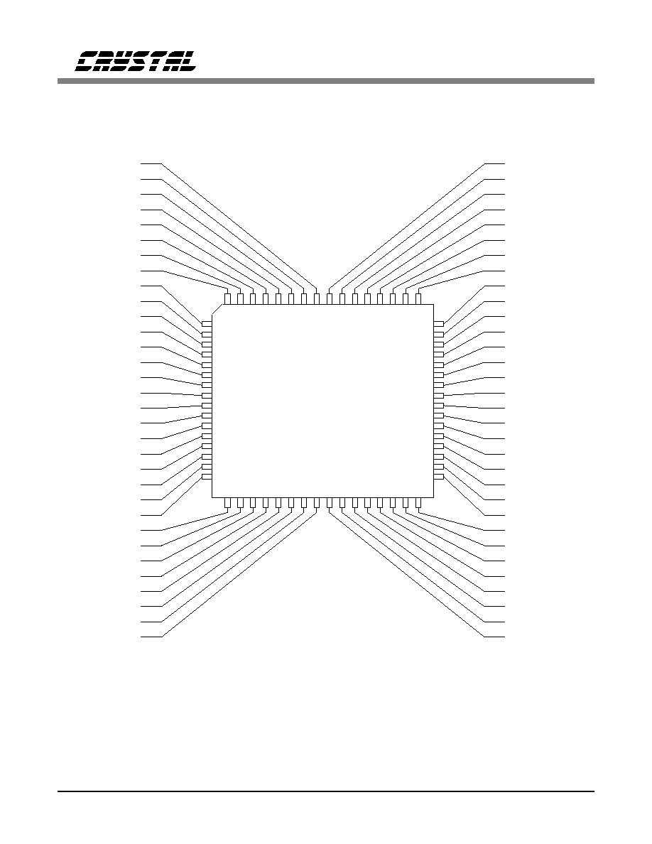
CS61583
64-Pin TQFP
Top View
46
44
42
40
38
36
48
34
18
20
22
24
26
28
30
32
64
62
60
58
56
54
52
50
1
4
6
8
10
12
14
2
16
DV+
DGND3
CON02
CON11
CON12
CON21
CON22
AMI1
RCLK2
RPOS2/RDATA2
RNEG2/BPV2
TCLK2
TPOS2/TDATA2
TNEG2/AIS2
LOS2
AMI2
J-TCK
J-TMS
TTIP2
TV+2
TGND2
TRING2
CODER2
CLKE
RTIP2
RRING2
RV+2
RGND2
1XCLK
RLOOP2
REFCLK
RESET
DGND1
CON01
TAOS2
TAOS1
LLOOP2
LLOOP1
RLOOP1
ATTEN1
RCLK1
RPOS1/RDATA1
RNEG1/BPV1
TCLK1
TPOS1/TDATA1
TNEG1/AIS1
LOS1
J-TDO
DGND2
J-TDI
TTIP1
TV+1
TGND1
TRING1
CODER1
ATTEN0
RTIP1
RRING1
RV+1
RGND1
AGND1
BGREF
AGND2
AV+
CS61583
24
DS172PP5

Power Supplies
AGND1, AGND2 : Analog Ground (PLCC pins 31, 33; TQFP pins 21, 23)
Analog supply ground pins.
AV+ : Analog Power Supply (PLCC pin 34; TQFP pin 24)
Analog supply pin for the internal bandgap reference and timing generation circuits.
BGREF : Bandgap Reference (PLCC pin 32; TQFP pin 22)
This pin is used by the internal bandgap reference and must be connected to ground
by a 4.99k
±
1% resistor to provide an internal current reference.
DGND1, DGND2, DGND3 : Digital Ground (PLCC pins 1, 18, 67; TQFP pins 57, 9, 55)
Power supply ground pins for the digital circuitry of both channels.
DV+ : Power Supply (PLCC pin 68; TQFP pin 56)
Power supply pin for the digital circuitry of both channels.
RGND1, RGND2 : Receiver Ground (PLCC pins 30, 39; TQFP pins 20, 29)
Power supply ground pins for the receiver circuitry.
RV+1, RV+2 : Receiver Power Supply (PLCC pins 29, 40; TQFP pins 19, 30)
Power supply pins for the analog receiver circuitry.
TGND1, TGND2 : Transmit Ground (PLCC pins 22, 47; TQFP pins 13, 36)
Power supply ground pins for the transmitter circuitry.
TV+1, TV+2 : Transmit Power Supply (PLCC pins 21, 48; TQFP pins 12, 37)
Power supply pins for the analog transmitter circuitry.
T1/E1 Data
RCLK1, RCLK2 : Receive Clock (PLCC pins 10, 59; TQFP pins 1, 48)
RPOS1, RPOS2 : Receive Positive Data (PLCC pins 11, 58; TQFP pins 2, 47)
RNEG1, RNEG2 : Receive Negative Data (PLCC pins 12, 57; TQFP pins 3, 46)
The receiver recovered clock and NRZ digital data from RTIP and RRING is output on these
pins. The CLKE pin determines the clock edge on which RPOS and RNEG are stable and
valid. A positive pulse (with respect to ground) received on RTIP generates a logic 1 on RPOS,
and a positive pulse received on RRING generates a logic 1 on RNEG.
RDATA1, RDATA2 : Receive Data (PLCC pins 11, 58; TQFP pins 2, 47)
In coder mode (CODER = 1), the decoded digital data stream from RTIP and RRING is output
on RDATA in NRZ format. The CLKE pin determines the clock edge on which RDATA is
stable and valid.
RTIP1, RTIP2 : Receive Tip (PLCC pins 27, 42; TQFP pins 17, 32)
RRING1, RRING2 : Receive Ring (PLCC pins 28, 41; TQFP pins 18, 31)
The receive AMI signal from the line interface is input on these pins. The recovered clock and
data are output on RCLK, RPOS, and RNEG (or RDATA).
CS61583
DS172PP5
25

TCLK1, TCLK2 : Transmit Clock (PLCC pins 13, 56; TQFP pins 4, 45)
TPOS1, TPOS2 : Transmit Positive Data (PLCC pins 14, 55; TQFP pins 5, 44)
TNEG1, TNEG2 : Transmit Negative Data (PLCC pins 15, 54; TQFP pins 6, 43)
The transmit clock and data are input to these pins. The signal is driven to the line interface at
TTIP and TRING. Data at TPOS and TNEG are sampled on the falling edge of TCLK. An
input at TPOS causes a positive pulse to be transmitted at TTIP and TRING, while an input at
TNEG causes a negative pulse to be transmitted at TTIP and TRING.
TDATA1, TDATA2 : Transmit Positive Data (PLCC pins 14, 55; TQFP pins 5, 44)
In coder mode (CODER = 1), the un-encoded digital data stream is input on TDATA in NRZ
format. Data at TDATA is sampled on the falling edge of TCLK.
TTIP1, TTIP2 : Transmit Tip (PLCC pins 20, 49; TQFP pins 11, 38)
TRING1, TRING2 : Transmit Ring (PLCC pins 23, 46; TQFP pins 14, 35)
The transmit AMI signal to the line interface is output on these pins. The transmit clock and
data are input from TCLK, TPOS, and TNEG (or TDATA).
Oscillator
1XCLK : One-times Clock Frequency Select (PLCC pin 38; TQFP pin 28)
When 1XCLK is set high, REFCLK must be a 1X clock (i.e., 1.544 MHz for T1 or 2.048 MHz
for E1 applications). When 1XCLK is set low, REFCLK must be an 8X clock (i.e., 12.352
MHz for T1 or 16.384 MHz for E1 applications).
REFCLK : External Reference Clock Input (PLCC pin 36, TQFP pin 26)
Input reference clock for the receive and jitter attenuator circuits. When 1XCLK is high,
REFCLK must be a 1X clock (i.e., 1.544 MHz
±100
ppm for T1 applications or 2.048 MHz
±
100 ppm for E1 applications). When 1XCLK is set low, REFCLK must be an 8X clock (i.e.,
12.352 MHz
±
100 ppm for T1 applications or 16.384 MHz
±
100 ppm for E1 applications). The
REFCLK input also determines the transmission rate when TAOS is asserted.
Control
AMI1, AMI2 : Encoder/Decoder Select (PLCC pins 61, 52; TQFP pins 49, 41)
Setting AMI low enables the B8ZS or HDB3 zero substitution in the transmitter encoders and
receiver decoders. Setting AMI high enables AMI encoders and decoders. The AMI pins are
enabled by setting the corresponding CODER pin high.
ATTEN0, ATTEN1 : Jitter Attenuator Select (PLCC pins 25, 8; TQFP pins 16, 64)
Selects the jitter attenuation path for both channels (transmit/receive/neither).
CLKE : Clock Edge (PLCC pin 44; TQFP pin 33)
Controls the polarity of the recovered clock RCLK. When CLKE is high, RPOS and RNEG are
valid on the falling edge of RCLK. When CLKE is low, RPOS and RNEG are valid on the
rising edge of RCLK.
CS61583
26
DS172PP5

CODER1, CODER2 : Coder Mode Configuration (PLCC pins 24, 45; TQFP pins 15, 34)
Setting CODER high causes the Coder Mode to be enabled. In Coder Mode, the transmit and
receive data appears in NRZ format on TDATA and RDATA, respectively. These pins also
enable the corresponding AMI pin.
CON01, CON11, CON21, : Configuration Selection
CON02, CON12, CON22 : (PLCC pins 2, 65, 63, 66, 64, 62; TQFP pins 58, 53, 51, 54, 52, 50)
These pins configure the transmitter (pulse shape, pulse width, pulse amplitude, and driver
impedance) receiver (slicing level), and coder (HDB3 vs B8ZS). The CONx1 pins control
channel 1 and the CONx2 pins control channel 2. Both channels must be configured to operate
at the same data rate on the line interface (both T1 or both E1).
LLOOP1, LLOOP2 : Local Loopback (PLCC pins 6, 5; TQFP pins 62, 61)
A local loopback is enabled when LLOOP is high. During local loopback, the TCLK,
TPOS/TNEG (or TDATA) inputs are looped back through the jitter attenuator (if enabled) to the
RCLK, RPOS/RNEG (or RDATA) outputs. The data at TPOS/TNEG continues to be
transmitted to the line interface unless overridden by a TAOS request. The inputs at RTIP and
RRING are ignored.
RESET : Reset (PLCC pin 35; TQFP pin 25)
A device reset is selected by setting the RESET pin high for a minimum of 200 ns. The reset
function initiates on the falling edge of RESET and requires less than 20 ms to complete. The
control logic is initialized and LOS is set high.
RLOOP1, RLOOP2 : Remote Loopback (PLCC pins 7, 37; TQFP pins 63, 27)
A remote loopback is selected when RLOOP is high. The data received from the line interface
at RTIP and RRING is looped back through the jitter attenuator (if enabled) and retransmitted
on TTIP and TRING. Data recovered from RTIP and RRING continues to be transmitted on
RPOS/RNEG (or RDATA). Data input on TPOS/TNEG (or TDATA) is ignored. A TAOS
request overrides the data transmitted at TTIP and TRING.
TAOS1, TAOS2 : Transmit All Ones Select (PLCC pins 4, 3; TQFP pins 60, 59)
Setting TAOS high causes continuous ones to be transmitted at the line interface on TTIP and
TRING at the frequency determined by REFCLK.
Status
AIS1, AIS2 : Alarm Indication Signal (PLCC pins 15, 54; TQFP pins 6, 43)
The AIS indication goes high when the receiver detects 99.9% ones density in a 5.3 ms period
(< 9 zeros in 8192 bits). The AIS indication returns low when the receiver detects
9
zeros in
8192 bits.
BPV1, BPV2 : Bipolar Violation (PLCC pins 12, 57; TQFP pins 3, 46)
The BPV indication goes high for one RCLK bit period when a bipolar violation is detected in
the received signal. Bipolar violations caused by B8ZS (or HDB3) zero substitutions are not
flagged by the BPV pin if the coder mode is enabled.
CS61583
DS172PP5
27

LOS1, LOS2 : Loss of Signal (PLCC pins 16, 53; TQFP pins 7, 42)
The LOS indication goes high when 175
±
15 consecutive zeros are received on the line
interface. The LOS indication returns low when a minimum 12.5% ones density signal over
175
± 75
bit periods with no more than 100 consecutive zeros is received
.
Test
J-TCK : JTAG Test Clock (PLCC pin 51; TQFP pin 40)
Data on pins J-TDI and J-TDO is valid on the rising edge of J-TCK. When J-TCK is stopped
low, all JTAG registers remain unchanged.
J-TMS : JTAG Test Mode Select (PLCC pin 50; TQFP pin 39)
An active high signal on J-TMS enables the JTAG serial port. This pin has an internal pull-up
resistor.
J-TDI : JTAG Test Data In (PLCC pin 19; TQFP pin 10)
JTAG data is shifted into the device on this pin. This pin has an internal pull-up resistor. Data
must be stable on the rising edge of J-TCK.
J-TDO : JTAG Test Data Out (PLCC pin 17; TQFP pin 8)
JTAG data is shifted out of the device on this pin. This pin is active only when JTAG testing is
in progress. J-TDO will be updated on the falling edge of J-TCK.
CS61583
28
DS172PP5
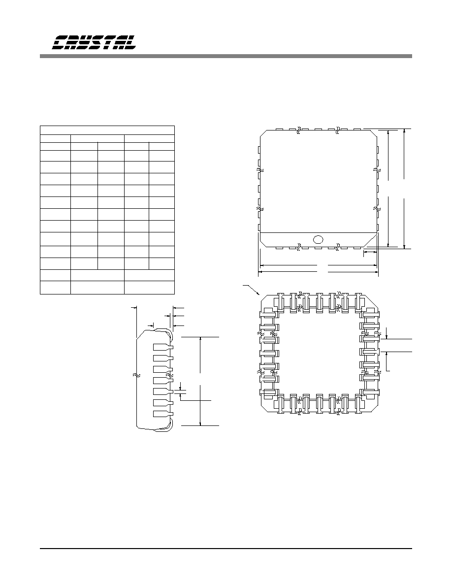
PHYSICAL DIMENSIONS
68 pin
PLCC
E
E
D
D
1
1
x
e
z
u
A
A1
y
B
E
MAX
MIN
MAX
MIN
MILLIMETERS
INCHES
DIM
A
5.08
4.20
.200
.165
D
D1
24.79
25.30
.976
.996
B
0.53
0.38
.021
.015
e
A
2.29
.090
1
24.13
24.38
.950
.960
1.27
.050
u
23.37
23.62
.920
.930
x
1.067
.042
E 1
y
z
.51
.020
.51 x 45∞ x 3
.02 x 45∞ x 3
3.30
.130
24.79
25.30
.976
.996
24.13
24.38
.950
.960
1.219
.048
68 pin PLCC
CS61583
DS172PP5
29
MILLIMETERS
INCHES
64
1
DIM
D
D
e
B
A
A
L
C
0.461
0.394
0.40
0.016
10.00
11.70
0.14
-
0.00
MIN
0.35
0.077
1.66
-
MAX
0.26
0.70
0.177
0.006
-
0.00
MIN
0.014
0.003
0.068
-
MAX
0.010
0.028
0.007
0.60
10.00
12.30
0.024
0.394
0.484
1
D
D
1
E
E
1
E
E
0.461
0.394
10.00
11.70
10.00
12.30
0.394
0.484
1
A
1
A
e
B
L
Terminal
Detail 1
C
1
0∞
12∞
0∞
12∞
64-Pin
TQFP
CS61583
30
DS172PP5

APPLICATIONS
Line Interface
Figure A1 illustrates a typical connection diagram
and Table A1 lists the external components that
are required in T1 and E1 applications.
In the transmit line interface circuitry, capacitors
C1 and C2 provide transmitter return loss. The
0.47
µ
F capacitor in series with the transformer
primary prevents output stage imbalances from
producing a DC current through the transformer
that might saturate the transformer and result in
an output level offset.
In the receive line interface circuitry, resistors R1-
R4 provide receive impedance matching and
receiver return loss. The 0.47
µ
F capacitor to
ground provides the necessary differential input
voltage reference for the receiver.
Power Supply
As shown in Figure A1, the CS61583 operates
from a 5.0 Volt supply. Separate analog and digi-
tal power supply and ground pins provide internal
isolation. The TGND, RGND, and DGND ground
pins must not be more negative than AGND. It is
recommended that all of the supply pins be con-
nected together at the device. A 4.99k
±
1%
AV+ AGND1:2 BGREF
TV+1
TGND1
RV+1 RGND1 DV+ DGND1:3
0.01
µ
F
TCLK1
TPOS1 (TDATA1)
TNEG1 (AIS1)
RCLK1
RPOS1 (RDATA1)
RNEG1 (BPV1)
TCLK2
TPOS2 (TDATA2)
TNEG2 (AIS2)
RCLK2
RPOS2 (RDATA2)
RNEG2 (BPV2)
Framer
Framer
TTIP1
TRING1
1:1.15
RTIP1
RRING1
TTIP2
TRING2
RTIP2
RRING2
1:1.15
Hardware Control
Power Supply
Clock Generator
Channel 2
Channel 1
transmit
transmit
3
0.1
µ
F
1
µ
F
+
0.1
µ
F
TV+2
TGND2
RV+2
RGND2
22
µ
F
+
0.1
µ
F
0.1
µ
F
0.1
µ
F
1:1.15
receive
R3
R4
1:1.15
receive
R1
R2
T1
T2
T3
T4
R3
4.99k
V
CC
0.47
µ
F
0.47
µ
F
REFCLK 1XCLK
RESET
CLKE
TAOS1
LLOOP1
RLOOP1
CON01
CON11
CON21
RLOOP2
LLOOP2
TAOS2
CON02
CON12
CON22
AMI2
AMI1
CODER2
CODER1
ATTEN1
ATTEN2
C1
C2
0.47
µ
F
0.47
µ
F
2
Figure A1. Typical Connection Diagram
Data Rate (MHz)
REFCLK Frequency (MHz)
Cable (
)
R1-R4 (
)
C1-C2 (pF)
1XCLK = 1
1XCLK = 0
1.544
1.544
12.352
100
38.3
220
2.048
2.048
16.384
75
28.7
470
120
45.3
220
Table A1. CS61583 External Components
CS61583
DS172PP5
31
resistor must be connected from BGREF to
ground to provide an internal current reference.
De-coupling and filtering of the power supplies is
crucial for the proper operation of the analog cir-
cuits. A capacitor should be connected between
each supply and its respective ground. For capaci-
tors smaller than 1
µ
F, use mylar or ceramic
capacitors and place them as close as possible to
their respective power supply pins. Wire-wrap
bread boarding of the line interface is not recom-
mended because lead resistance and inductance
defeat the function of the de-coupling capacitors.
Crystal Oscillator Specifications
When a reference clock signal is not available, a
CMOS crystal oscillator operating at either the
1X or 8X rate can be connected at the REFCLK
pin. The oscillator must have a minimum symme-
try of 40-60% and minimum stability of
±
100
ppm for T1 and E1 applications. Based on these
specifications, some suggested crystal oscillators
for use with the CS61583 are shown in Table A2.
Transformers
Recommended transformer specifications are
shown in Table A3. Based on these specifications,
the transformers recommended for use with the
CS61583 are listed in Table A4.
Designing for AT&T 62411
For additional information on the requirements of
AT&T 62411 and the design of an appropriate
system synchronizer, refer to the Crystal Semi-
conductor Application Notes "AT&T 62411
Design Considerations - Jitter and Synchroniza-
ti o n " a nd "J i t te r Test in g Pro c e d u r e s f o r
Compliance with AT&T 62411."
Line Protection
Secondary protection components can be added
to the line interface circuitry to provide lightning
surge and AC power-cross immunity. For addi-
tional information on the different electrical
safety standards and specific application circuit
recommendations, refer to the Crystal Semicon-
ductor Application Note "Secondary Line
Protection for T1 and E1 Line Cards."
Turns Ratio
1:1.15 step-up transmit
1:1.15 step-down receive
Primary inductance
1.5 mH min at 772 kHz
Primary leakage
inductance
0.3
µ
H max at 772 kHz
with secondary shorted
Secondary leakage
inductance
0.4
µ
H max at 772 kHz
Interwinding
capacitance
18 pF max, primary to
secondary
ET-constant
16 V-
µ
s min
Table A3. Transformer Specifications
Manufacturer
Part Number
Contact Number
Comclok
CT31CH
(800) 333-9825
CTS
CXO-65HG-5-I (815) 786-8411
M-tron
MH26TAD
(800) 762-8800
SaRonix
NTH250A
(800) 227-8974
Notes:
Frequency tolerances are
±
32 ppm with a -40 to +85 ∞C
operating temperature range.
All are 8-pin DIP packages and can be tristated.
Table A2. Suggested Crystal Oscillators
CS61583
32
DS172PP5

Schematic & Layout Review Service
Confirm Optimum
Schematic & Layout
Before Building Your Board.
For Our Free Review Service
Call Applications Engineering.
C a l l : ( 5 1 2 ) 4 4 5 - 7 2 2 2
Turns Ratio
Manufacturer
Part Number
Package Type
1:1.15
Pulse Engineering
PE-65388
1.5 kV through-hole, single
PE-65770
1.5 kV through-hole, single
extended temperature
PE-65838
3.0 kV through-hole, single
extended temperature
PE-68674
1.5 kV surface-mount, dual
extended temperature
PE-65870
1.5 kV surface-mount, dual
Schott
67124840
1.5 kV through-hole, single
extended temperature
Valor
ST5112
2.0 kV surface mount, dual
CS61583
DS172PP5
33
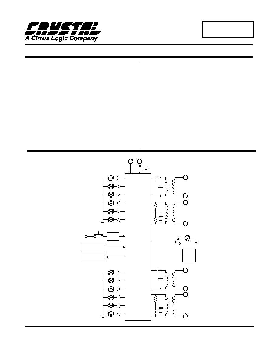
Features
∑
∑
Socketed CS61583 Dual Line Interface
∑
∑
All Required Components for CS61583
Evaluation
∑
∑
Locations to Evaluate Protection Circuitry
∑
∑
LED Status Indications for Alarm
Conditions
∑
∑
Control of Enhanced Hardware Options
General Description
The evaluation board includes a socketed CS61583
dual line interface device and all support components
necessary for evaluation. The board is powered by
an external +5 Volt supply.
The board may be configured for 100
twisted-pair
T1, 75
coax E1, or 120
twisted-pair E1 operation.
Binding posts and bantam jacks are provided for line
interface connections. Several BNC connectors pro-
vide clock and data I/O at the system interface.
Reference timing may be derived from a crystal oscil-
lator or an external reference clock. Four LED
indicators monitor device alarm conditions.
ORDERING INFORMATION: CDB61583
DEC '95
DB172PP1
34
Crystal Semiconductor Corporation
P.O. Box 17847, Austin, TX 78760
(512) 445-7222 FAX: (512) 445 7581
Dual Line Interface Evaluation Board
CDB61583
Copyright
©
Crystal Semiconductor Corporation 1995
(All Rights Reserved)
Oscillator
Circuit
TTIP1
TRING1
RTIP1
RRING1
TTIP2
TRING2
RTIP2
RRING2
}
CHANNEL 1
}
CHANNEL 2
+5V
0V
TCLK1
TPOS1
(TDATA1)
TNEG1
RCLK1
RPOS1
(RDATA1)
RNEG1
(BPV1)
{
CHANNEL 1
RESET
CIRCUIT
+5V
TCLK2
TPOS2
(TDATA2)
TNEG2
RCLK2
RPOS2
(RDATA2)
RNEG2
(BPV2)
CHANNEL 2
Hardware Control
and Mode Circuit
LED Status
Indicators
{
CS61583
REFCLK

POWER SUPPLY
As shown on the evaluation board schematic in
Figures 1-5, power is supplied to the board from
an external +5 Volt supply connected to the two
binding posts labeled V+ and GND. Zener diode
Z1 protects the components on the board from
reversed supply connections and over-voltage
damage. Capacitor C16 provides power supply
decoupling and ferrite bead L1 isolates the
CS61583 and buffer supplies. Both sides of the
evaluation board contain extensive areas of
ground plane to insure optimum performance.
Capacitors C3, C5-C8, C13, C18, and C38
provide power supply decoupling for the
CS61583. The BGREF pin is pulled down
through resistor R10 to provide an internal
current reference. The buffers are decoupled
using capacitors C9, C15, and C19. Ferrite beads
L2-L4 help reduce the power supply noise that is
coupled from the buffers to the power supply.
BOARD CONFIGURATION
The evaluation board is based on the CDB61584
used to evaluate the CS61584 dual LIU
optimized for Host mode applications. Because
the CS61583 is optimized for Hardware mode
applications, slide switch SW6 must be placed in
the "HW" position to set the AGND1 pin of the
CS61583 to a logic 0. In addition, the host
processor interface appearing at J26 is not used
on the CDB61583.
The evaluation board is configured using DIP
switches SW2, SW3, and SW4. Because the
evaluation board is based on the CDB61584
design, switches SW2, SW3, and SW4 are
relabeled with white stickers. These switches
establish the digital control inputs for both line
interface channels. Closing a DIP switch towards
the label sets the CS61583 control pin of the
same name to a logic 1. All switch inputs are
pulled-down using resistor networks RP2-RP5.
The CDB61583 switch functions are listed
below:
∑
TAOS1, TAOS2: transmit all ones;
∑
LLOOP1, LLOOP2: local loopback;
∑
RLOOP1, RLOOP2: remote loopback;
∑
CODER1, CODER2: encoder/decoder control;
∑
ATTEN0, ATTEN1: jitter attenuator selection;
∑
CLKE: RCLK edge polarity;
∑
1XCLK: clock frequency selection;
∑
AMI1, AMI2: encoder/decoder control;
∑
CONx1, CONx2: line configuration settings.
A jumper must be installed on header J10 to
enable RLOOP2 functionality.
Alarm Indications
The LOS1 and LOS2 LED indicators illuminate
when the line interface receiver has detected a
loss of signal. Headers J7 and J13 must be
jumpered in the "TNEG" position to provide
connectivity to the BNC input when the coder
mode is disabled (CODER(1,2) = 0).
The AIS alarm condition is provided when the
coder mode is enabled (CODER(1,2) = 1) and
headers J7 and J13 are jumpered in the "AIS"
position. The AIS1 and AIS2 LED indicators
illuminate when the line interface receiver has
detected the all-ones receive input signal.
Resistors R26 and R27 pull-down the
TNEG(1,2) inputs when coder mode is disabled
but headers J7 and J13 are jumpered in the
"AIS" position.
Manual Reset
A momentary contact switch SW1 provides a
manual reset by forcing the RESET pin of the
CS61583 to a logic 1. Although the transmit and
receive circuitry are continuously calibrated, the
CDB61583
DB172PP1
35

reset can be used to initialize the control logic.
Both channels are powered up after exiting reset.
TRANSMIT CIRCUIT
The transmit clock and data signals are supplied
on BNC inputs labeled TCLK(1,2), TPOS(1,2),
and TNEG(1,2). When the coder mode is
disabled, data is supplied on the TPOS(1,2) and
TNEG(1,2) BNC inputs in RZ format. When the
coder mode enabled, data is supplied on the
TDATA(1,2) BNC input in NRZ format and the
TNEG(1,2) BNC input may be used to indicate
the AIS alarm condition as described in the
Board Configuration section.
The transmitter output is transformer coupled to
the line interface through 1:1.15 step-up
transformers T1 and T4. The signal is available
at either the TTIP(1,2) and TRING(1,2) binding
posts or the TX(1,2) bantam jacks.
Capacitors C2 and C11 prevent output stage
imbalances from producing a DC current that
may saturate the transformer and result in an
output level offset. Capacitors C1 and C12
provide transmitter return loss and are socketed
so the value may be changed according to the
application. A 220 pF capacitor is required for
100
twisted-pair T1 or 120
twisted-pair E1
applications. A 470 pF capacitor is required for
75
coax E1 applications. These capacitors are
included with the evaluation board.
Optional diode locations D6-D9 and D10-D13
and optional resistor locations R8-R9 and
R18-R19 provide test locations to evaluate
transmit line interface protection circuitry.
RECEIVE CIRCUIT
The receive signal is input at either the
RTIP(1,2) and RRING(1,2) binding posts or the
RX(1,2) bantam jacks. The receive signal is
transformer coupled to the CS61583 through
1:1.15 step-down transformers T2 and T3.
The receive line is terminated by resistors R3-R4
and R14-R15 to provide impedance matching
and receiver return loss. They are socketed so
the values may be changed according to the
application. The evaluation board is supplied
from the factory with 38.3
resistors for
terminating
100
twisted-pair T1 lines, 45.3
resistors for terminating 120
twisted-pair E1
lines, and 28.7
resistors
for terminating 75
coaxial E1 lines. Capacitors C4 and C10 provide
a differential input voltage reference.
Optional resistor locations R1-R2, R12-R13,
R16-R17, and R24-R25 provide test locations to
evaluate receive line interface protection
circuitry.
The recovered clock and data signals are
available on BNC outputs labeled RCLK(1,2),
RPOS(1,2), and RNEG(1,2). When the coder
mode is disabled, data is available on the
RPOS(1,2) and RNEG(1,2) BNC outputs in RZ
format. When the coder mode is enabled, data is
available on the RDATA(1,2) BNC output in
NRZ format and bipolar violations are reported
on BPV(1,2).
REFERENCE CLOCK
The CDB61583 requires a T1 or E1 reference
clock for operation. This clock may operate at
either a 1-X rate (1.544 MHz or 2.048 MHz) or
an 8-X rate (12.352 MHz or 16.384 MHz) and
can be supplied by either a crystal oscillator or
an external reference. The evaluation board is
supplied from the factory with two crystal
oscillators for T1 and E1 operation.
CDB61583
36
DB172PP1

Crystal Oscillator
A crystal oscillator may be inserted at socket U4
in the orientation indicated by the silkscreen.
Header J14 must be jumpered in the "OSC"
position to provide connectivity to the REFCLK
pin of the CS61583. The SW2 switch position
labeled "1XCLK" must be open (logic 0) for 8-X
clock operation or closed (logic 1) for 1-X clock
operation.
External Reference
An external reference may be provided at the
REFCLK BNC input. Header J14 must be
jumpered in the "REFCLK" position to provide
connectivity to the REFCLK pin of the
CS61583. The SW2 switch position labeled
"1XCLK" must be open (logic 0) for 8-X clock
operation or closed (logic 1) for 1-X clock
operation.
BUFFERING
Buffers U2 and U3 provide additional drive
capability for the BNC inputs and outputs. The
buffer outputs are filtered with an RC network to
reduce the transients caused by buffer switching.
JTAG ACCESS
The CS61583 implements JTAG boundary scan
to support board-level testing. Interface port J56
provides access to the four JTAG pins on the
CS61583. The J-TMS pin of the CS61583 is
pulled-down by resistor R28 to disable boundary
scan unless the pin is externally pulled high
using the interface port.
TRANSFORMER SELECTION
The evaluation board is supplied from the
factory with Pulse Engineering PE-65388
transformers installed at locations T1-T4. They
are socketed to permit the evaluation of other
transformers.
LINE PROTECTION EVALUATION
Several optional resistor and diode locations on
the transmit and receive line interface allow for
the installation and evaluation of various types
of protection circuitry. Each location is drilled
with 60 mil vias to permit the installation of
sockets. These sockets can be obtained from
McKenzie at (510) 651-2700 by requesting part
#PPC-SIP-1X32-620C and are identical to the
socket type installed at various resistor locations
on the board. They allow the line protection
circuitry to be easily changed during testing.
Note that the traces forming shorts between the
socket locations on the line interface may need
to be cut prior to protection circuitry installation.
PROTOTYPING AREA
Four prototyping areas with power supply and
ground connections are provided on the
evaluation board. These areas can be used to
develop and test a variety of additional circuits
such as framer devices, system synchronizer
PLLs, or specialized interface logic.
EVALUATION HINTS
1. The orientation of pin 1 for the CS61583 is
labeled "1" on the left side of the socket U7.
2. A jumper must be placed on header J10 when
using the CDB61583.
3. Component locations R3-R4, R14-R15, C1,
and C12 must have the correct values installed
according to the application. All the necessary
components are included with the evaluation
board.
CDB61583
DB172PP1
37

4. Closing a DIP switch on SW2, SW3, and
SW4 towards the label sets the CS61583 control
pin of the same name to logic 1.
5. When performing a manual loopback of the
recovered signal to the transmit signal at the
BNC connectors, the recovered data must be
valid on the falling edge of RCLK to properly
latch the data in the transmit direction. To
accomplish this, the SW2 switch position labeled
"CLKE" must be closed (logic 1).
6. Jumpers can be placed on headers J9 and J12
to provide a ground reference on TRING for
75
coax E1 applications.
7. Properly terminate TTIP/TRING when
evaluating the transmit output pulse shape. For
more information concerning pulse shape
evaluation, refer to the Crystal application note
entitled "Measurement and Evaluation of Pulse
Shapes in T1/E1 Transmission Systems."
CDB61583
38
DB172PP1

R C L K 1
R P O S 1
R N E G 1
T C L K 1
T P O S 1
T N E G 1
L O S 1
J -T D O
D G N D 2
J -T D I
T T IP 1
T V + 1
T G N D 1
T R IN G 1
C O D E R 1
A T T E N 0
RT
I
P
1
RRI
NG
1
1 0
1 1
1 2
1 3
1 4
1 5
R C L K 1
R P O S 1
R N E G 1
T C L K 1
T P O S
T N E G
3
5
7
4
6
8
1 7
1 5
1 3
1 6
1 4
1 2
U 2
U 2
U 2
U 2
U 2
U 2
2
4
1
3
J 7
R 2 6
4 7 K
1
R 6
4 7 0
D 1
L E D
A IS 1
1
R 7
4 7 0
D 2
L E D
L O S 1
V A +
2
2
V A +
3
3
Q 1
Q 2
J-T D O
V D +
J -T D I
C 3
.1
µ
F
C O D E R 1
A T T E N 0
1 6
1 7
1 8
1 9
2 0
2 1
2 2
2 3
2 4
2 5
C 1
C 2
.4 7
µ
F
V D +
V D +
2
6
1
5
3
T 1
1
T
R
J 8 A
J 3 1
J 3 2
T T IP 1
T R IN G 1
J 9
2
6
1
5
3
T 2
6
9
T
R
J 8 B
J 3 3
J 3 4
R T IP 1
R R IN G 1
C 4
R 4
R 3
C 9
.1
µ
F
V C C
2 0
1 0
U 2
1
1 9
27
28
G N D
U 7
C S61583
CH AN N E L 1
J 1
J 2
J 3
J 4
J 5
J 6
R 2 9
R 3 0
R 3 1
C 2 6
C 2 7
C 2 8
C 2 9
C 3 0
C 3 1
R 5
R 3 8
R 3 9
L 4
V A +
2 6 N /C -1
R 8
R 9
R 2 4
R 2 5
.4 7
µ
F
1 .1 5 :1
P E -6 5 3 8 8
1 .1 5 :1
P E -6 5 3 8 8
T V + 1
N o te s : C o m p o n e n ts R 3 , R 4 , a n d C 1 a re s o c k e te d to p e rm it v alu e c h a n g e s
to th e a p p lic a tio n .
C o m p o n e n t lo c a tio n s R 1 , R 2, R 8 , R 9 , R 2 4 , R 2 5 , an d D 1 0 -D 1 3 p ro v id e
a re a s fo r e v a lu a tin g p ro te c tio n c irc u itry.
5 1 .1
5 1 .1
5 1 .1
1 0 0 p F
1 0 0 p F
1 0 0 p F
1 0 0 p F
1 0 0 p F
1 0 0 p F
(R D A T A 1 )
(B P V 1 )
(T D A T A 1 )
E N A
E N A
5 1 .1
5 1 .1
5 1 .1
4
R 1
R 2
D 1 3
D 1 2
D 1 1
D 1 0
Figure 1. Channel 1 Circuitry
CDB61583
DB172PP1
39
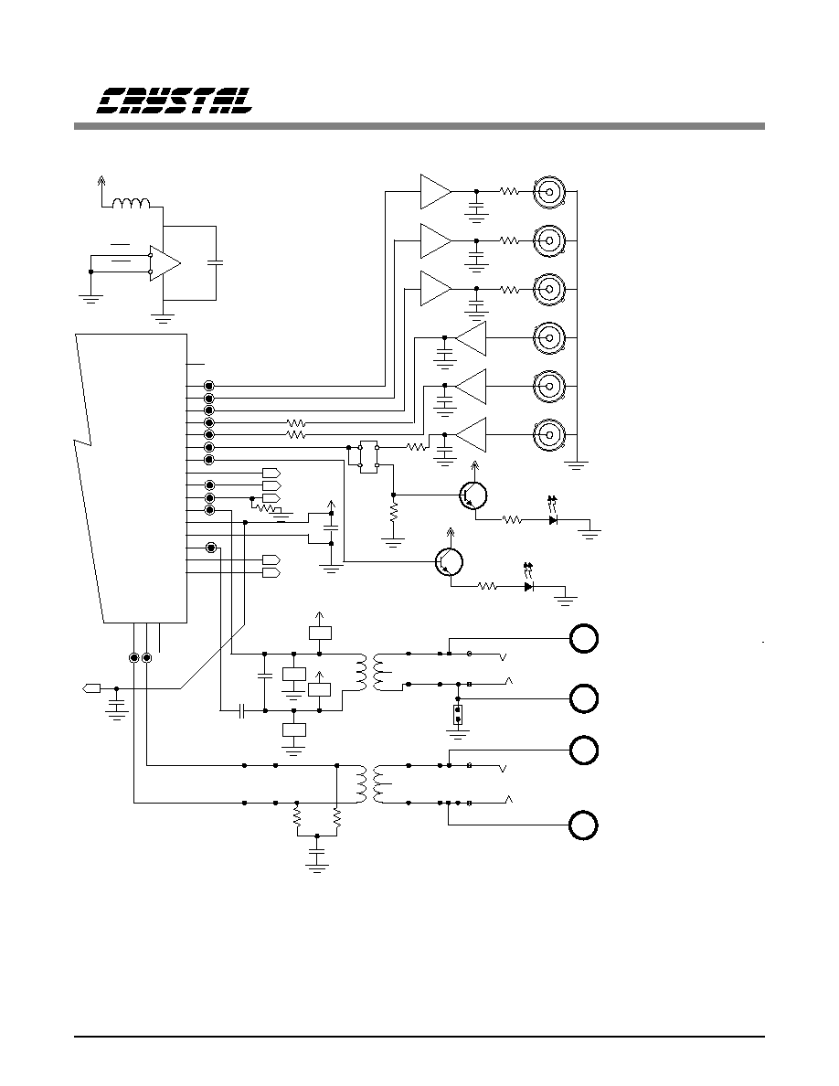
R C L K 2
R P O S 2
R N E G 2
T C L K 2
T P O S 2
T N E G 2
L O S 2
A M I2
J-T C K
J -T M S
T T IP 2
T V + 2
T G N D 2
T R IN G 2
C O D E R 2
C L K E
RT
I
P
2
RRI
NG2
U 7
C S 61583
C H A N N E L 2
5 9
5 8
5 7
5 6
5 5
5 4
R C L K 2
R P O S 2
R N E G 2
T C L K 2
T P O S 2
T N E G 2
9
7
5
6
4
2
1 1
1 3
1 5
1 4
1 6
1 8
U 3
U 3
U 3
U 3
U 3
U 3
R 2 2
1
3
2
4
J1 3
R 2 7
4 7 K
1
R 2 0
4 7 0
D 3
L E D
A IS 2
1
R 2 1
4 7 0
D 4
L E D
L O S 2
V A +
2
2
3
3
Q 3
Q 4
A M I2
V D +
J-T M S
C 1 3
.1
µ
F
C O D E R 2
C L K E
5 3
5 2
5 1
5 0
4 9
4 8
4 7
4 6
4 5
4 4
C 1 2
C 1 1
.4 7
µ
F
V D +
2
6
1
5
3
T 4
6
9
T
R
J1 1 B
J2 7
J2 8
T T IP 2
T R IN G 2
J 1 2
2
6
1
5
3
T 3
1
4
T
R
J1 1 A
J2 9
J3 0
R T IP 2
R R IN G 2
C 1 0
.4 7
µ
F
R 1 5
R 1 4
C 1 5
.1
µ
F
V C C
2 0
1 0
U 3
1
1 9
42
41
G N D
J-T C K
1 0 K
V A +
L 2
N /C -3
6 0
N/
C-
2
43
R 5 0
R 5 1
C 3 2
C 3 3
C 3 4
C 3 5
C 3 6
C 3 7
R 4 1
R 4 2
R 4 3
J1 6
J1 7
J 1 8
J1 9
J 2 0
J 2 1
V A +
V D +
1 :1 .1 5
P E -6 5 3 8 8
1 :1 .1 5
P E -6 5 3 8 8
R 1 6
R 1 7
R 1 2
R 1 3
T V +1
C 3 8
2 2
µ
F
E N A
E N A
1 0 0 p F
5 1 .1
(R D A T A 2 )
(B P V 2 )
(T D A T A 2 )
1 0 0 p F
1 0 0 p F
1 0 0 p F
1 0 0 p F
5 1 .1
5 1 .1
5 1 .1
5 1 .1
R 2 8
5 1 .1
R 1 8
R 1 9
N otes : C om po nents R 14, R 15, an d C 12 a re sock eted to perm it value changes acc ordin g
to th e applic ation.
C om ponent loc ations R 12, R 13, R 16-R 1 9, and D 6-D 9 provide area s for ev aluatin g
p rotec tion circuitry.
1 0 0 p F
D 6
D 7
D 9
D 8
Figure 2. Channel 2 Circuitry
CDB61583
40
DB172PP1

2
4
6
8
1 0
1 2
1 4
1 6
1 8
2 0
2 2
2 4
2 6
AT
TEN
1
RL
OO
P
1
LL
O
O
P
1
LL
O
O
P
2
TA
O
S
1
TA
O
S
2
CO
N0
1
DG
ND
1
DV
+
DG
ND
3
CO
N0
2
CO
N1
1
CO
N1
2
CO
N2
1
CO
N2
2
AM
I
1
U 7
CS61584
C ON TRO L C IR CU ITR Y
1
2 4 T A O S 2
2
2 3 T A O S 1
3
2 2 L L O O P 2
4
2 1 L L O O P 1
5
2 0 R L O O P 1
6
1 9 C O D E R 1
7
1 8 C O D E R 2
8
1 7 A T T E N 0
9
1 6 A T T E N 1
1 0
1 5 C L K E
1 1
1 4 1 X C L K
1 2
1 3
V D +
S W 2
U 6
U 6
9
U 6
6
1 8
2
1 6
4
A T T E N 0
C L K E
1 X C L K
C 1 8
.0 1
µ
F
V D +
1
3
5
7
9
1 1
1 3
1 5
1 7
1 9
2 1
2 3
2 5
SC
LK
SD1
CS
S D 0
J 2 6
9
1 1
J -T D 0
J -T D 1
J -T M S
T -T C K
2
4
6
8
1
3
5
7
J 5 6
4 7 k
1
2
3
4
5
6
R P 2
8
1
C O N 0 1
7
2
C O N 1 1
6
3
C O N 2 1
5
4
A M I1
V D +
S W 3
8
1
C O N 0 2
7
2
C O N 1 2
6
3
C O N 2 2
5
4
A M I2
S W 4
2
3
4
5
6
1
R P 3
A M I2
U 6
1 3
U 6
C 2 5
C 3 9
R 5 8
R 5 7
C 2 0
R
5
9
C 2 3
C 2 4
N/
C-
4
8
7
6
5
4
3
2
1
61
4 7 k
V D +
J 2 4
R 5 5
3 .9 2 k
5 1 .1
R 5 6
IN T
1 0 0 p F
1 0 0 p F
5 1 .1
R P 4
8
4 7 k
1 0 0 p F
5 1 .1
1 0 0
p F
1 0 0 p F
5 1 .1
51
.
1
68
67
66
65
64
63
62
1 4
G N D
R 4 0
G N D
G N D
G N D
R P 5
4 7 k
7 6 5 4 3 2
8 7 6 5 4 3 2
1
1
7
R L O O P 2
R L O O P 2
C O D E R 1
C O D E R 2
N o te : T h e H ost inte rfa ce at J26 is n ot used o n the C D B 61 583.
Figure 3. Control Circuitry
CDB61583
DB172PP1
41
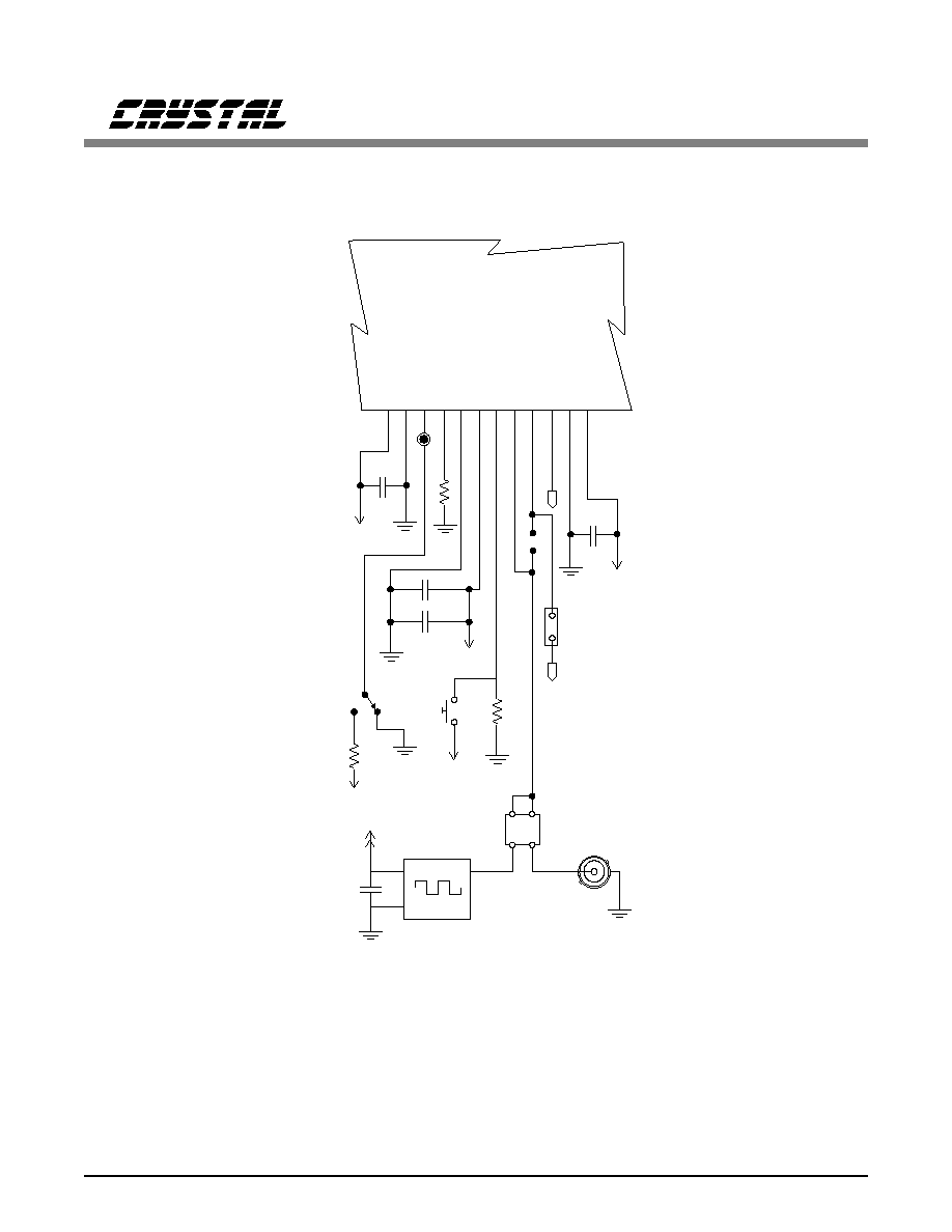
RV+
1
RG
ND1
AG
N
D
1
BG
R
E
F
AG
N
D
2
AV+
RESET
REFCL
K
R
L
OOP
2
1X
C
L
K
RG
ND2
RV+
2
U 7
C S61583
TIMING CIRCUITR Y
29
40
C 5
.1
µ
F
V D +
R 2 3
47 K
R1
0
4.
99k
C 6
C 7
.1
µ
F
1 .0
µ
F
V D +
V D +
V D +
S W 1
1
2
R 11
10 K
Y 1
1X
C
L
K
4
2
1
3
J14
8
V C C
G N D
C 14
.1
µ
F
U 4
R E F C L K
J15
C 8
.1
µ
F
V D +
J 10
(m ust be jum pe red)
V A +
30
31
32
33
34
35
36
37
38
39
S W 6
R L O O P 2
N otes: A crystal o scillator at U 4 o r e xtern al refere nce sup plied a t J15 m ust be p rovided .
A qu artz crystal cann ot b e use d w ith the C S 6 158 3
Figure 4. Timing Circuitry
CDB61583
42
DB172PP1
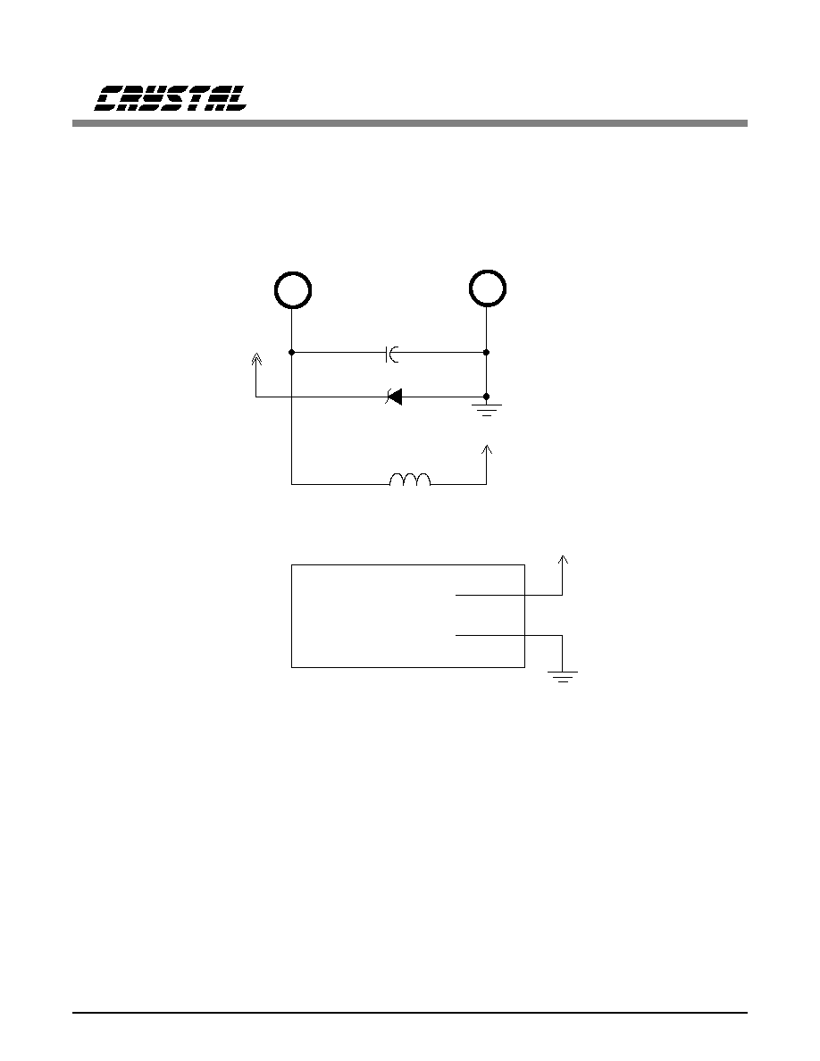
V A +
V D +
J22
J23
V +
G N D
C 1 6
L 1
V D +
P ro totyp ing A re a
Z 1
4 7
µ
F
Figure 5. Common Circuitry
CDB61583
DB172PP1
43

Smart
Analog
TM
is a Trademark of Crystal Semiconductor Corporation