 | –≠–Ľ–Ķ–ļ—ā—Ä–ĺ–Ĺ–Ĺ—č–Ļ –ļ–ĺ–ľ–Ņ–ĺ–Ĺ–Ķ–Ĺ—ā: XCB170 | –°–ļ–į—á–į—ā—Ć:  PDF PDF  ZIP ZIP |
Part #
Description
XCB170
6 Pin DIP (50/Tube)
XCB170S
6 Pin Surface Mount (50/Tube)
XCB170STR
6 Pin Surface Mount (1000/Reel)
XCB170
Units
Load Voltage
350
V
Load Current
100
mA
Max R
ON
50
www.clare.com
DS-XBA170-R2.0
XCB170
Single Pole OptoMOS
ģ
Relays
1
Applications
Features
Description
Approvals
Ordering Information
Pin Configuration
∑
Telecommunications
∑
Telecom Switching
∑
Tip/Ring Circuits
∑
Modem Switching (Laptop, Notebook, Pocket
Size)
∑
Hookswitch
∑
Dial Pulsing
∑
Ground Start
∑
Ringer Injection
∑
Instrumentation
∑
Multiplexers
∑
Data Acquisition
∑
Electronic Switching
∑
I/O Subsystems
∑
Meters (Watt-Hour, Water, Gas)
∑
Medical Equipment-Patient/Equipment Isolation
∑
Security
∑
Aerospace
∑
Industrial Controls
∑
Small 6 Pin DIP Package
∑
Low Drive Power Requirements (TTL/CMOS
Compatible)
∑
No Moving Parts
∑
High Reliability
∑
Arc-Free With No Snubbing Circuits
∑
3750V
RMS
Input/Output Isolation
∑
No EMI/RFI Generation
∑
Machine Insertable, Wave Solderable
∑
Surface Mount and Tape & Reel
Versions Available
The XCB170 is a 1-Form-B relay which uses optically
coupled MOSFET technology to provide 3750V of
input to output isolation. The efficient MOSFET switch-
es and photovoltaic die use Clare's patented
OptoMOS
ģ
architecture. A highly efficient GaAIAs
infrared LED controls the optically coupled input. The
device is available in small 6-pin dual in line package
in standard through hole and surface mount lead bend.
∑
UL Recognized: File Number E76270
∑
CSA Certified: File Number LR 43639-10
∑
BSI Certified to:
∑
BS EN 60950:1992 (BS7002:1992)
Certificate #: 7344
∑
BS EN 41003:1993
Certificate #: 7344
1
3
2
4
5
6
+ Control
≠ Control
Do Not Use
Load
Do Not Use
Load
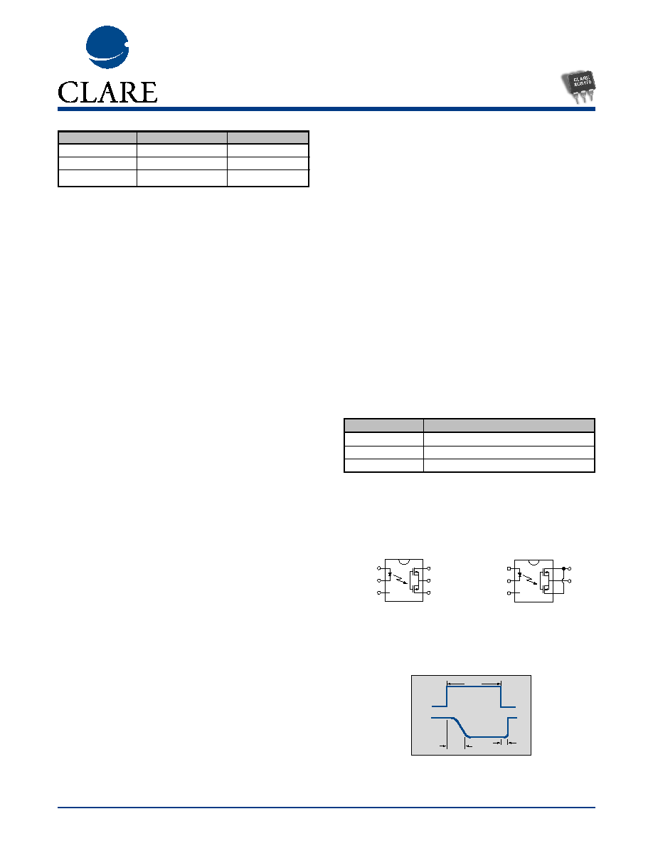
AC/DC Configuration
XCB170 Pinout
1
3
2
4
5
6
+ Control
≠ Control
Do Not Use
+ Load
≠ Load
DC Only Configuration
XCB170 Pinout
Switching Characteristics of
Normally Closed (Form B) Devices
CONTROL
10ms
10%
90%
90%
+
+
T
ON
T
OFF
+
Parameter
Conditions
Symbol
Min
Typ
Max
Units
Output Characteristics @ 25įC
Load Voltage (Peak)
-
V
L
-
-
350
V
Load Current (Continuous)
AC/DC Configuration
-
I
L
-
-
100
mA
DC Configuration
-
I
L
-
-
180
mA
Peak Load Current
10ms
I
LPK
-
-
350
mA
On-Resistance
AC/DC Configuration
I
L
=120mA
R
ON
-
31
50
DC Configuration
I
L
=200mA
R
ON
-
10
15
Off-State Leakage Current
V
L
=35OV
I
LEAK
-
-
1
ĶA
Switching Speeds
Turn-On
I
F
=5mA, V
L
=10V
T
ON
-
-
5
ms
Turn-Off
I
F
=5mA, V
L
=10V
T
OFF
-
-
5
ms
Output Capacitance
50V; f=1MHz
C
OUT
-
25
-
pF
Capacitance
Input to Output
-
-
-
3
-
pF
Input Characteristics @ 25įC
Input Control Current
I
L
=120mA
I
F
5
-
50
mA
Input Dropout Current
-
I
F
0.4
0.7
-
mA
Input Voltage Drop
I
F
=5mA
V
F
0.9
1.2
1.4
V
Reverse Input Voltage
-
V
R
-
-
5
V
Reverse Input Current
V
R
=5V
I
R
-
-
10
ĶA
Input to Output Capacitance
-
C
I/O
-
3
-
pF
Parameter
Min
Typ Max Units
Input Power Dissipation
-
-
150
1
mW
Input Control Current
-
-
50
mA
Peak (10ms)
-
-
1
A
Reverse Input Voltage
-
-
5
V
Total Power Dissipation
-
-
800
2
mW
Isolation Voltage
Input to Output
3750
-
-
V
RMS
Operational Temperature
-40
-
+85
įC
Storage Temperature
-40
-
+125
įC
Soldering Temperature
DIP Package
-
-
+260
įC
Surface Mount Package
-
-
+220
įC
(10 Seconds Max.)
1
Derate Linearly 1.33 mw/įC
2
Derate Linearly 6.67 mw/įC
www.clare.com
2
XCB170
Rev. 2.0
Absolute Maximum Ratings are stress ratings. Stresses in
excess of these ratings can cause permanent damage to
the device. Functional operation of the device at these or
any other conditions beyond those indicated in the opera-
tional sections of this data sheet is not implied. Exposure of
the device to the absolute maximum ratings for an extend-
ed period may degrade the device and effect its reliability.
Absolute Maximum Ratings (@ 25į C)
Electrical Characteristics
XCB170
www.clare.com
3
Rev. 2.0
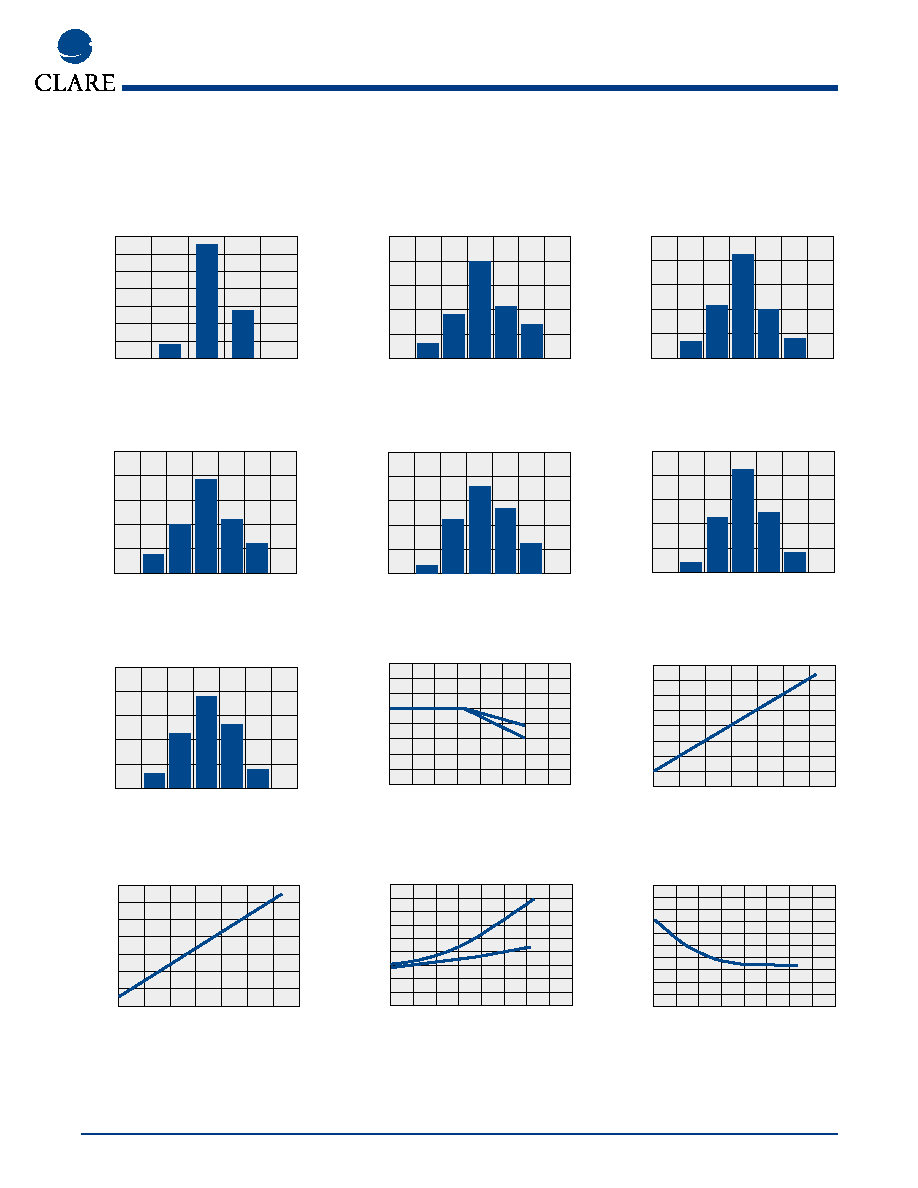
PERFORMANCE DATA*
* The Performance data shown in the graphs above is typical of device performance. For guaranteed parameters not indicated in the written specifications, please contact our application
department.
XCB170
Typical LED Forward Voltage Drop
(N=50 Ambient Temperature = 25
įC)
I
F
= 5mADC
35
30
25
20
15
10
5
0
1.17
1.19
1.21
1.23
1.25
LED Forward Voltage Drop (V)
Device Count (N)
XCB170
Typical On-Resistance Distribution
(N=50 Ambient Temperature = 25
įC)
(Load Current = 100mADC)
25
20
15
10
5
0
29.09
30.63
32.16
33.70
29.86
31.40
32.93
On-Resistance (
)
Device Count (N)
XCB170
Typical Blocking Voltage Distribution
(N=50 Ambient Temperature = 25
įC)
25
20
15
10
5
0
424.0
434.5
444.9
455.4
429.3
439.7
450.1
Blocking Voltage (V)
Device Count (N)
XCB170
Typical I
F
for Switch Operation
(N=50 Ambient Temperature = 25
įC)
(Load Current = 100mADC)
0.50
0.62
0.75
0.44
0.56
0.69
0.81
LED Current (mA)
Device Count (N)
25
20
15
10
5
0
XCB170
Typical I
F
for Switch Dropout
(N=50 Ambient Temperature = 25
įC)
(Load Current = 100mADC
25
20
15
10
5
0
0.50
0.62
0.75
0.44
0.56
0.69
0.81
LED Current (mA)
Device Count (N)
)
XCB170
Typical Turn-Off Time
(N=50 Ambient Temperature = 25
įC)
(Load Current = 100mADC)
0.67
0.83
0.99
1.14
0.75
0.91
1.06
Turn-On (ms)
Device Count (N)
25
20
15
10
5
0
XCB170
Typical Blocking Voltage
vs. Temperature
Temperature (
įC)
Blocking Voltage (V
RMS
)
-40
455
450
445
440
435
430
425
420
-20
0
20
40
60
80
100
XCB170
Typical Turn-Off vs. Temperature
(Load Current = 100mADC)
Temperature (
įC)
5mA
10mA
Turn-On (ms)
-40
1.80
1.60
1.40
1.20
1.00
0.80
0.60
0.40
0.20
0
-20
0
20
40
60
80
100
120
XCB170
Typical Turn-On Time
(N=50 Ambient Temperature = 25
įC)
(Load Current = 100mADC)
0.11
0.17
0.22
0.28
0.25
0.19
0.14
Turn-Off (ms)
Device Count (N)
25
20
15
10
5
0
XCB170
Typical Load Current vs. Temperature
Temperature (
įC)
Load Current (mA)
160
140
120
100
80
60
40
20
0
-40
-20
0
20
40
60
80
120
100
10mA
5mA
XCB170
Typical Leakage vs. Temperature
(Measured across Pins 4 & 6)
Temperature (
įC)
Leakage (
Ķ
A)
-40
0.016
0.014
0.012
0.010
0.008
0.006
0.004
0.002
0
-20
0
20
40
60
80
100
XCB170
Typical Turn-On vs. Temperature
(Load Current = 100mADC)
Temperature (
įC)
Turn-Off (ms)
-40
0.50
0.45
0.40
0.35
0.30
0.25
0.20
0.15
0.10
0.05
0
-20
0
20
40
60
80
100
120
I
F
= 5mA
www.clare.com
4
XCB170
Rev. 2.0
PERFORMANCE DATA*
* The Performance data shown in the graphs above is typical of device performance. For guaranteed parameters not indicated in the written specifications, please contact our application
department.
XCB170
Typical LED Forward Voltage Drop
vs. Temperature
Temperature (
įC)
LED Forward Voltage Drop (V)
1.8
1.6
1.4
1.2
1.0
0.8
-40
-20
0
20
40
60
80
120
100
50mA
10mA
5mA
XCB170
Typical Turn-Off vs. LED Forward Current
(Load Current = 100mADC)
LED Forward Current (mA)
Turn-On (ms)
0
5
10
15
20
25
30
35
40
45
2.0
1.8
1.6
1.4
1.2
1.0
0.8
0.6
0.4
0.2
0
50
XCB170
Typical Turn-On vs. LED Forward Current
(Load Current = 100mADC)
LED Forward Current (mA)
Turn-Off (ms)
0
5
10
15
20
25
30
35
40
45
1.0
0.9
0.8
0.7
0.6
0.5
0.4
0.3
0.2
0.1
0
50
XCB170
Typical On-Resistance vs. Temperature
(Load Current = 100mADC; I
F
= 5mA)
Temperature (
įC)
On-Resistance (
)
-40
70
60
50
40
30
20
10
0
-20
0
20
40
60
80
100
120
XCB170
Typical I
F
for Switch Operation
vs. Temperature
(Load Current = 50mA)
Temperature (
įC)
LED Current (mA)
-40
6.0
5.0
4.0
3.0
2.0
1.0
0
-20
0
20
40
60
80
100
120
XCB170
Typical I
F
for Switch Dropout
vs. Temperature
(Load Current = 50mA)
Temperature (
įC)
LED Current (mA)
-40
6.0
5.0
4.0
3.0
2.0
1.0
0
-20
0
20
40
60
80
100
120
XCB170
Typical Load Current vs. Load Voltage
(Ambient Temperature = 25
įC)
I
F
= 5mADC
Load Voltage (V)
Load Current (mA)
120
100
80
60
40
20
0
-20
-40
-60
-80
-100
-120
-3
-4
-2
-1
0
1
2
3
4
XCB170
Energy Rating Curve
Time
Load Current (A)
10
Ķs
1.0
0.9
0.8
0.7
0.6
0.5
0.4
0.3
0.2
0.1
0
1ms
100
Ķs
100ms
1s
10ms
10s
100s
XCB170
www.clare.com
5
Rev. 2.0
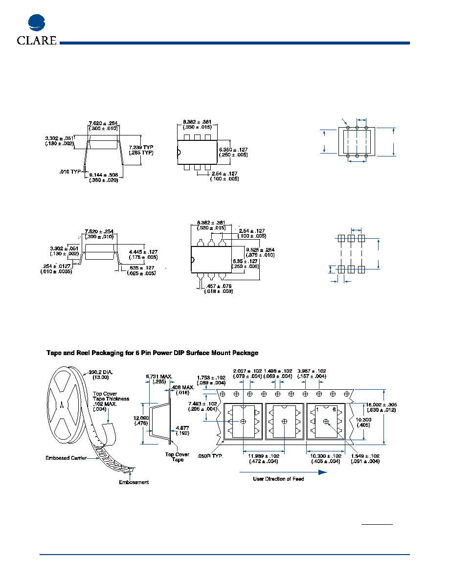
Dimensions
mm
(inches)
MECHANICAL DIMENSIONS
PC Board Pattern
(Top View)
2.540
Ī .127
(.100
Ī .005)
8.305
Ī .127
(.327
Ī .005)
1.905
Ī .127
(.075
Ī .005)
1.499
Ī .127
(.059
Ī .005)
PC Board Pattern
(Top View)
6.350
Ī .127
(.250
Ī .005)
2.540
Ī .127
(.100
Ī .005)
7.620
Ī .127
(.300
Ī .005)
5.080
Ī .127
(.200
Ī .005)
6-.800 DIA.
(6-.031 DIA.)
6Pin DIP Through Hole (Standard)
6Pin DIP Surface Mount ("S" Suffix)
Clare, Inc. makes no representations or warranties with respect to the accuracy or completeness of the contents of this publication and reserves the right to make changes to specifications and product descriptions
at any time without notice. Neither circuit patent licenses nor indemnity are expressed or implied. Except as set forth in Clare's Standard Terms and Conditions of Sale, Clare, Inc. assumes no liability whatsoever, and
disclaims any express or implied warranty, relating to its products including, but not limited to, the implied warranty of merchantability, fitness for a particular purpose, or infringement of any intellectual property right.
The products described in this document are not designed, intended, authorized or warranted for use as components in systems intended for surgical implant into the body, or in other applications intended to sup-
port or sustain life, or where malfunction of Clare's product may result in direct physical harm, injury, or death to a person or severe property or environmental damage. Clare, Inc. reserves the right to discontinue or
make changes to its products at any time without notice.
Specification: DS-XCB170-R2.0
©Copyright 2001, Clare, Inc.
OptoMOS
ģ
is a registered trademark of Clare, Inc.
All rights reserved. Printed in USA.
9/26/01
For additional information please visit our website at: www.clare.com