9-Mb Pipelined SRAM with QDRTM Architecture
CY7C1304V25
Cypress Semiconductor Corporation
∑
3901 North First Street
∑
San Jose
∑
CA 95134
∑
408-943-2600
Document #: 38-05167 Rev. *A
Revised August 15, 2002
Features
∑ Separate independent Read and Write data ports
-- Supports concurrent transactions
∑ 167 MHz Clock for high bandwidth
-- 2.5 ns Clock-to-Valid access time
∑ 4-Word burst for reducing address bus frequency
∑ Double Data Rate (DDR) interfaces on both Read & Write
Ports (data transferred at 333 MHz) @167 MHz
∑ Two input clocks (K and K)
[1]
for precise DDR timing
-- SRAM uses rising edges only
∑ Two output clocks (C and C) accounts for clock skew
and flight time mis-matches
∑ Single multiplexed address input bus latches address
inputs for both READ and WRITE ports
∑ Separate Port Selects for depth expansion
∑ Synchronous internally self-timed writes
∑ 2.5V core power supply with HSTL Inputs and Outputs
[1]
∑ 13x15 mm 1.0 mm pitch fBGA package, 165 ball (11x15
matrix)
∑ Variable drive HSTL output buffers
∑ Expanded HSTL output voltage (1.4V-1.9V)
∑ JTAG Interface
Functional Description
The CY7C1304V25 is a 2.5V Synchronous Pipelined SRAM
equipped with QDR architecture. QDR architecture consists of
two separate ports to access the memory array. The Read port
has dedicated Data Outputs to support Read operations and
the Write Port has dedicated Data Inputs to support Write op-
erations. QDR architecture has separate data inputs and data
outputs to completely eliminate the need to "turn-around" the
data bus required with common I/O devices. Access to each
port is accomplished through a common address bus. Ad-
dresses for Read and Write addresses are latched on alter-
nate rising edges of the input (K)
[1]
clock. Accesses to the
CY7C1304V25 Read and Write ports are completely indepen-
dent of one another. In order to maximize data throughput,
both Read and Write ports are equipped with Double Data
Rate (DDR) interfaces. Each address location is associated
with 4 18-bit words that burst sequentially into or out of the
device. Since data can be transferred into and out of the de-
vice on every rising edge of both input clocks (K/K
[1]
and C/C)
memory bandwidth is maximized while simplifying system de-
sign by eliminating bus "turn-arounds".
Depth expansion is accomplished with Port Selects for each
port. Port selects allow each port to operate independently.
All synchronous inputs pass through input registers controlled
by the K or K
[1]
input clocks. Data outputs pass through output
registers controlled by the C or C input clocks. Writes are con-
ducted with on-chip synchronous self-timed write circuitry.
Selection Guide
7C1304V25-167
7C1304V25-133
7C1304V25-100
Maximum Operating Frequency (MHz)
167
133
100
Maximum Operating Current (mA)
450
350
230
Note:
1.
K and K inputs require V
IH
to be greater than V
REF
+ 0.5V and V
IL
to be less than V
REF
- 0.5. This is a subset of JEDEC standards for HSTL I/Os.
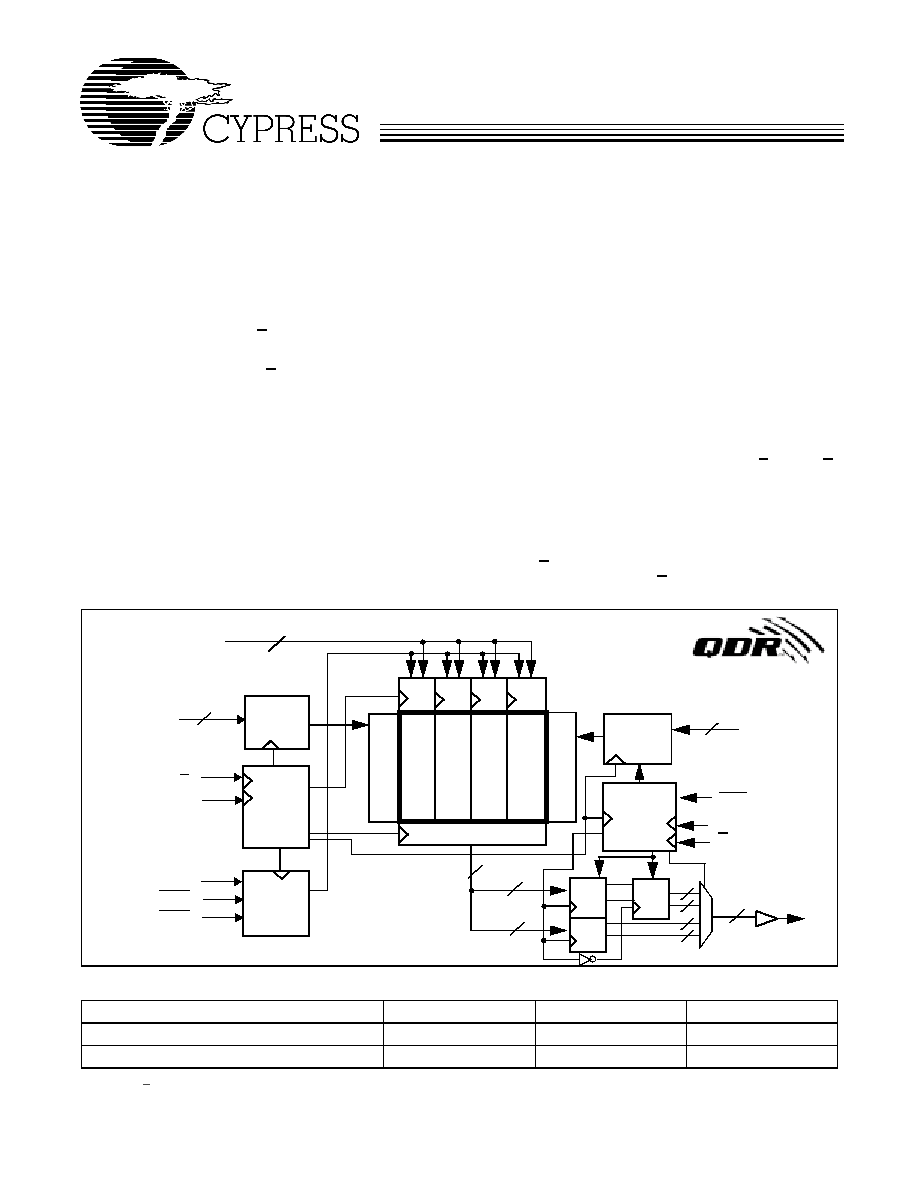
Logic Block Diagram
12
8Kx1
8 Arr
a
y
CLK
A
(16:0)
Gen.
K
[1]
K
[1]
Control
Logic
Address
Register
D
[17:0]
R
e
a
d
A
dd.
D
e
c
ode
Read Data Reg.
RPS
WPS
Q
[17:0]
Control
Logic
Address
Register
Reg.
Reg.
Reg.
36
17
18
72
18
BWS
[0:1]
Vref
W
r
it
e Add.
D
e
c
ode
Write
Reg
36
A
(16:0)
17
C
C
12
8Kx1
8 Arr
a
y
12
8Kx1
8 Arr
a
y
12
8Kx1
8 Arr
a
y
Write
Reg
Write
Reg
Write
Reg
18

CY7C1304V25
Document #: 38-05167 Rev. *A
Page 2 of 24
Pin Configuration
1
2
3
4
5
6
7
8
9
10
11
A
NC
Gnd/
144M
NC/
36M
WPS
BWS
1
K
[1]
NC
RPS
NC/
18M
Gnd/
72M
NC
B
NC
Q9
D9
A
NC
K
[1]
BWS
0
A
NC
NC
Q8
C
NC
NC
D10
VSS
A
NC
A
VSS
NC
Q7
D8
D
NC
D11
Q10
VSS
VSS
VSS
VSS
VSS
NC
NC
D7
E
NC
NC
Q11
VDDQ
VSS
VSS
VSS
VDDQ
NC
D6
Q6
F
NC
Q12
D12
VDDQ
VDD
VSS
VDD
VDDQ
NC
NC
Q5
G
NC
D13
Q13
VDDQ
VDD
VSS
VDD
VDDQ
NC
NC
D5
H
NC
VREF
VDDQ
VDDQ
VDD
VSS
VDD
VDDQ
VDDQ
VREF
ZQ
J
NC
NC
D14
VDDQ
VDD
VSS
VDD
VDDQ
NC
Q4
D4
K
[1]
NC
NC
Q14
VDDQ
VDD
VSS
VDD
VDDQ
NC
D3
Q3
L
NC
Q15
D15
VDDQ
VSS
VSS
VSS
VDDQ
NC
NC
Q2
M
NC
NC
D16
VSS
VSS
VSS
VSS
VSS
NC
Q1
D2
N
NC
D17
Q16
VSS
A
A
A
VSS
NC
NC
D1
P
NC
NC
Q17
A
A
C
A
A
NC
D0
Q0
R
TDO
TCK
A
A
A
C
A
A
A
TMS
TDI
CY7C1304V25
(Top View)

CY7C1304V25
Document #: 38-05167 Rev. *A
Page 3 of 24
Pin Definitions
Name
I/O
Description
D
[17:0]
Input-
Synchronous
Data input signals, sampled on the rising edge of K and K
[1]
clocks during valid write
operations.
WPS
Input-
Synchronous
Write Port Select, active LOW. Sampled on the rising edge of the K
[1]
clock. When
asserted active, a write operation is initiated. Deasserting will deselect the Write port.
Deselecting the Write port will cause D
[17:0]
to be ignored.
BWS
0
, BWS
1
Input-
Synchronous
Byte Write Select 0 and 1, active LOW. Sampled on the rising edge of the K and K
[1]
clocks during write operations. Used to select which byte is written into the device during
the current portion of the write operations. Bytes not written remain unaltered.BWS
0
controls D
[8:0]
while BWS
1
controls D
[17:9].
BWS
0
and BWS
1
are sampled on the same
edge as D
[17:0]
. Deselecting a Byte Write Select will cause the corresponding byte of
data to be ignored and not written into the device.
A
Input-
Synchronous
Address Inputs. Sampled on the rising edge of the K
[1]
clock during active read and
write operations. These address inputs are multiplexed for both Read and Write oper-
ations. Internally, the device is organized 128K x 72. Therefore, only 17 address inputs
are needed to access the entire memory array.These inputs are ignored when the ap-
propriate port is deselected.
Q
[17:0]
Outputs-
Synchronous
Data Output signals. These pins drive out the requested data during a Read operation.
Valid data is driven out on the rising edge of both the C and C clocks during Read
operations or K and K
[1]
. when in single clock mode. When the Read port is deselected,
Q
[17:0]
are automatically three-stated.
RPS
Input-
Synchronous
Read Port Select, active LOW. Sampled on the rising edge of Positive Input Clock
(K)
[1]
. When active, a Read operation is initiated. Deasserting will cause the Read port
to be deselected. When deselected, the pending access is allowed to complete and the
output drivers are automatically three-stated following the next rising edge of the C
clock. The CY7C1304V25 is organized internally as 128K x 72. Each read access con-
sists of a burst of four sequential 18-bit transfers.
C
Input-Clock
Positive Output Clock Input. C is used in conjunction with C to clock out the Read
data from the device. C and C can be used together to deskew the flight times of various
devices on the board back to the controller. See application example for further details.
C
Input-Clock
Negative Output Clock Input. C is used in conjunction with C to clock out the Read
data from the device. C and C can be used together to deskew the flight times of various
devices on the board back to the controller. See application example for further details.
K
[1]
Input-Clock
Positive Input Clock Input. The rising edge of K is used to capture synchronous inputs
to the device and to drive out data through Q
[17:0]
when in single clock mode. All ac-
cesses are initiated on the rising edge of K.
K
[1]
Input-Clock
Negative Input Clock Input. K
[1]
is used to capture synchronous inputs being present-
ed to the device and to drive out data through Q
[17:0]
when in single clock mode.
ZQ
Input
Output Impedance Matching Input. This input is used to tune the device outputs to
the system data bus impedance. Q
[17:0]
output impedance are set to 0.2 x RQ, where
RQ is a resistor connected between ZQ and ground. Alternately, this pin can be con-
nected directly to V
DD
, which enables the minimum impedance mode. This pin cannot
be connected directly to GND or left unconnected.
TDO
Output
TDO for JTAG.
TCK
Input
TCK pin for JTAG.
TDI
Input
TDI pin for JTAG.
TMS
Input
TMS pin for JTAG.
NC/18M
Input
Address expansion for 18M. This is not connected to the die.
NC/36M
Input
Address expansion for 36M. This is not connected to the die.
GND/72M
Input
Address expansion for 72M. This should be tied LOW on the CY7C1304V25
GND/144M
Input
Address expansion for 144M. This should be tied LOW on the CY7C1304V25

CY7C1304V25
Document #: 38-05167 Rev. *A
Page 4 of 24
Introduction
Functional Overview
The CY7C1304V25 is a synchronous pipelined Burst SRAM
equipped with both a Read Port and a Write Port. The Read
port is dedicated to Read operations and the Write Port is ded-
icated to Write operations. Data flows into the SRAM through
the Write port and out through the Read Port. The
CY7C1304V25 multiplexes the address inputs in order to min-
imize the number of address pins required. By having separate
Read and Write ports, the CY7C1304V25 completely elimi-
nates the need to "turn-around" the data bus and avoids any
possible data contention, thereby simplifying system design.
Each access consists of 4 18-bit data transfers in two clock
cycles.
Accesses for both ports are initiated on the Positive Input
Clock (K)
[1]
. All synchronous input timing is referenced from
the rising edge of the input clocks (K and K)
[1]
and all output
timing is referenced to the output clocks (C and C or K and K
[1]
when in single clock mode).
All synchronous data inputs (D
[17:0]
) inputs pass through input
registers controlled by the input clocks (K and K)
[1]
. All syn-
chronous data outputs (Q
[17:0]
) outputs pass through output
registers controlled by the rising edge of the output clocks (C
and C or K and K
[1]
when in single clock mode).
All synchronous control (RPS, WPS, BWS
0
, BWS
1
) inputs
pass through input registers controlled by the rising edge of
the input clocks (K and K
[1]
, C and C).
Read Operations
The CY7C1304V25 is organized internally as a 128Kx72
SRAM. Accesses are completed in a burst of four sequential
18-bit data words. Read operations are initiated by asserting
RPS
active at the rising edge of the Positive Input Clock (K)
[1]
.
The address presented to Address inputs are stored in the
Read address register. Following the next K
[1]
clock rise the
corresponding lowest order 18-bit word of data is driven onto
the Q
[17:0]
using C as the output timing reference. On the sub-
sequent rising edge of C the next 18-bit data word is driven
onto the Q
[17:0]
. This process continues until all four 18-bit data
words have been driven out onto Q
[17:0]
. The requested data
will be valid 2.5ns from the rising edge of the output clock (C
or C, 167MHz device). In order to maintain the internal logic,
each read access must be allowed to complete. Each Read
access consists of 4 18-bit data words and takes 2 clock cycles
to complete. Therefore, Read accesses to the device can not
be initiated on two consecutive K
[1]
clock rises. The internal
logic of the device will ignore the second Read request. Read
accesses can be initiated on every other K
[1]
clock rise. Doing
so will pipeline the data flow such that data is transferred out
of the device on every rising edge of the output clocks (C and
C or K and K
[1]
when in single clock mode).
When the read port is deselected, the CY7C1304V25 will first
complete the pending read transactions. Synchronous internal
circuitry will automatically three-state the outputs following the
next rising edge of the Negative Output Clock (C). This will
allow for a seamless transition between devices without the
insertion of wait states in a depth expanded memory.
Write Operations
Write operations are initiated by asserting WPS active at the
rising edge of the Positive Input Clock (K)
[1]
. On the following
K
[1]
clock rise the data presented to D
[17:0]
is latched and
stored into the lower 18-bit Write Data register provided
BWS
[1:0]
are both asserted active. On the subsequent rising
edge of the Negative Input Clock (K)
[1]
the information pre-
sented to D
[17:0]
is also stored into the Write Data Register
provided BWS
[1:0]
are both asserted active. This process con-
tinues for one more cycle until 4 18-bit words (a total of 72 bits)
of data are stored in the SRAM. The 72 bits of data are then
written into the memory array at the specified location. There-
fore, Write accesses to the device can not be initiated on two
consecutive K
[1]
clock rises. The internal logic of the device will
ignore the second Write request. Write accesses can be initi-
ated on every other rising edge of the Positive Input Clock
(K)
[1]
. Doing so will pipeline the data flow such that 18-bits of
data can be transferred into the device on every rising edge of
the input clocks (K and K)
[1]
.
When deselected, the write port will ignore all inputs after the
pending Write operations have been completed.
Byte Write Operations
Byte Write operations are supported by the CY7C1304V25. A
write operation is initiated as described in the Write Operation
section above. The bytes that are written are determined by
BWS
0
and BWS
1
which are sampled with each set of 18-bit
data word. Asserting the appropriate Byte Write Select input
during the data portion of a write will allow the data being pre-
sented to be latched and written into the device. De-asserting
the Byte Write Select input during the data portion of a write
will allow the data stored in the device for that byte to remain
unaltered. This feature can be used to simplify READ/MODI-
FY/WRITE operations to a Byte Write operation.
Single Clock Mode
The CY7C1304V25 can be used with a single clock that con-
trols both the input and output registers. In this mode the de-
vice will recognize only a single pair of input clocks (K and K)
[1]
that control both the input and output registers. This operation
V
REF
Input-
Reference
Reference Voltage Input. Static input used to set the reference level for HSTL inputs
[1]
and Outputs as well as A/C measurement points.
V
DD
Power Supply
Power supply inputs to the core of the device. Should be connected to 2.5V power
supply.
V
SS
Ground
Ground for the device. Should be connected to ground of the system.
V
DDQ
Power Supply
Power supply inputs for the outputs of the device. Should be connected to 1.5V
power supply.
NC
NC
No connect
Pin Definitions
(continued)
Name
I/O
Description

CY7C1304V25
Document #: 38-05167 Rev. *A
Page 5 of 24
is identical to the operation if the device had zero skew be-
tween the K/K
[1]
and C/C clocks. All timing parameters remain
the same in this mode. To use this mode of operation, the user
must tie C and C HIGH at power on. This function is a strap
option and not alterable during device operation.
Concurrent Transactions
The Read and Write ports on the CY7C1304V25 operate com-
pletely independently of one another. Since each port latches
the address inputs on different clock edges, the user can Read
or Write to any location, regardless of the transaction on the
other port. If the ports access the same location at the same
time, the SRAM will deliver the most recent information asso-
ciated with the specified address location. This includes for-
warding data from a Write cycle that was initiated on the pre-
vious K
[1]
clock rise.
Read accesses and Write access must be schedule such that
one transaction is initiated on any clock cycle. If both ports are
selected on the same K
[1]
clock rise, the arbitration depends
on the previous state of the SRAM. If both ports were dese-
lected, the Read port will take priority. If a Read was initiated
on the previous cycle, the Write port will assume priority (since
Read operations can not be initiated on consecutive cycles).
If a Write was initiated on the previous cycle, the Read port will
assume priority (since Write operations can not be initiated on
consecutive cycles). Therefore, asserting both port selects ac-
tive from a deselected state will result in alternating
Read/Write operations being initiated, with the first access be-
ing a Read.
Depth Expansion
The CY7C1304V25 has a Port Select input for each port. This
allows for easy depth expansion. Both Port Selects are sam-
pled on the rising edge of the Positive Input Clock only (K)
[1]
.
Each port select input can deselect the specified port. Dese-
lecting a port will not affect the other port. All pending transac-
tions (Read and Write) will be completed prior to the device
being deselected.
Programmable Impedance
An external resistor, RQ, must be connected between the ZQ
pin on the SRAM and V
SS
to allow the SRAM to adjust its
output driver impedance. The value of RQ must be 5X the
value of the intended line impedance driven by the SRAM, The
allowable range of RQ to guarantee impedance matching with
a tolerance of ±10% is between 175
and 350
,
with
V
DDQ
=1.5V. The output impedance is adjusted every 1024 cy-
cles to adjust for drifts in supply voltage and temperature.