 | –≠–ª–µ–∫—Ç—Ä–æ–Ω–Ω—ã–π –∫–æ–º–ø–æ–Ω–µ–Ω—Ç: CY7C1352 | –°–∫–∞—á–∞—Ç—å:  PDF PDF  ZIP ZIP |

256K x18 Pipelined SRAM with NoBLTM Architecture
CY7C1352
Cypress Semiconductor Corporation
∑
3901 North First Street
∑
San Jose
∑
CA 95134
∑
408-943-2600
August 9, 1999
Features
∑ Pin compatible and functionally equivalent to ZBTTM
devices MCM63Z818 and MT55L256L18P
∑ Supports 143-MHz bus operations with zero wait states
-- Data is transferred on every clock
∑ Internally self-timed output buffer control to eliminate
the need to use OE
∑ Fully registered (inputs and outputs) for pipelined
operation
∑ Byte Write Capability
∑ 256K x 18 common I/O architecture
∑ Single 3.3V power supply
∑ Fast clock-to-output times
-- 4.0 ns (for 143-MHz device)
-- 4.2 ns (for 133-MHz device)
-- 5.0 ns (for 100-MHz device)
-- 7.0 ns (for 80-MHz device)
∑ Clock Enable (CEN) pin to suspend operation
∑ Synchronous self-timed writes
∑ Asynchronous output enable
∑ JEDEC-standard 100-pin TQFP package
∑ Burst Capability--linear or interleaved burst order
∑ Low standby power
Functional Description
The CY7C1352 is a 3.3V 256K by 18 synchronous-pipelined
Burst SRAM designed specifically to support unlimited true
back-to-back Read/Write operations without the insertion of
wait states. The CY7C1352 is equipped with the advanced No
Bus LatencyTM (NoBLTM) logic required to enable consecutive
Read/Write operations with data being transferred on every
clock cycle. This feature dramatically improves the throughput
of the SRAM, especially in systems that require frequent
Read/Write transitions.The CY7C1352 is pin/functionally com-
patible to ZBTTM SRAMs MCM63Z819 and MT55L256L18P.
All synchronous inputs pass through input registers controlled
by the rising edge of the clock. All data outputs pass through
output registers controlled by the rising edge of the clock. The
clock input is qualified by the Clock Enable (CEN) signal, which
when deasserted suspends operation and extends the previ-
ous clock cycle. Maximum access delay from the clock rise is
4.0 ns (143-MHz device).
Write operations are controlled by the four Byte Write Select
(BWS
[1:0]
) and a Write Enable (WE) input. All writes are con-
ducted with on-chip synchronous self-timed write circuitry.
Three synchronous Chip Enables (CE
1
, CE
2
, CE
3
) and an
asynchronous Output Enable (OE) provide for easy bank se-
lection and output three-state control. In order to avoid bus
contention, the output drivers are synchronously three-stated
during the data portion of a write sequence.
.
NoBL and No Bus Latency are trademarks of Cypress Semiconductor Corporation.
ZBT is a trademark of Integrated Device Technology.
CLK
A
[17:0]
CEN
WE
BWS
CE1
CE
CE2
OE
OUT
P
UT
256Kx18
MEMORY
ARRAY
CL
K
Logic Block Diagram
DQ
[15:0]
Data-In REG.
Q
D
CE
CONTROL
and WRITE
LOGIC
3
[1:0]
RE
GI
S
T
E
R
S
an
d LO
G
I
C
ADV/LD
18
18
18
18
18
18
DP
[1:0]
Mode
Selection Guide
7C1352-143
7C1352-133
7C1352-100
7C1352-80
Maximum Access Time (ns)
4.0
4.2
5.0
7.0
Maximum Operating Current (mA)
Commercial
450
400
350
300
Maximum CMOS Standby Current (mA)
Commercial
5
5
5
5
CY7C1352
2
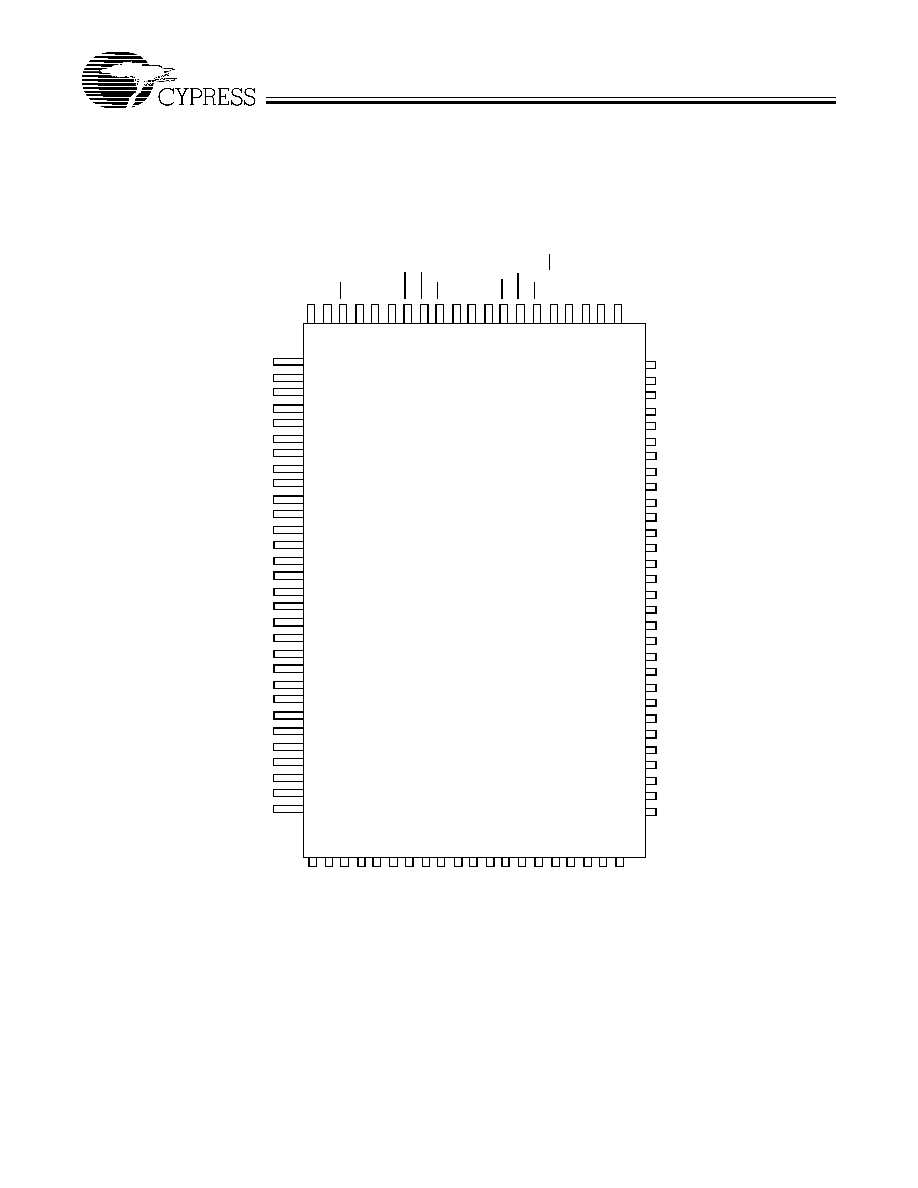
Pin Configuration
100-Pin TQFP
A
5
A
4
A
3
A
2
A
1
A
0
DNU
DNU
V
SS
V
DD
DNU
A
10
A
11
A
12
A
13
A
14
A
16
A
17
NC
NC
V
DDQ
V
SS
NC
DP
0
DQ
7
DQ
6
V
SS
V
DDQ
DQ
5
DQ
4
V
SS
V
DD
V
DD
DQ
3
DQ
2
V
DDQ
V
SS
DQ
1
DQ
0
NC
NC
V
SS
V
DDQ
NC
NC
NC
NC
NC
NC
V
DDQ
V
SS
NC
NC
DQ
8
DQ
9
V
SS
V
DDQ
DQ
10
DQ
11
V
DDQ
V
DD
V
DD
V
SS
DQ
12
DQ
13
V
DDQ
V
SS
DQ
14
DQ
15
DP
1
NC
V
SS
V
DDQ
NC
NC
NC
A6
A7
CE
1
CE
2
NC
NC
BW
S
1
BW
S
0
CE
3
V
DD
V
SS
CL
K
WE
CE
N
OE
NC
A
8
A
9
1
2
3
4
5
6
7
8
9
10
11
12
13
14
15
16
17
18
19
20
21
22
23
24
25
26
27
28
29
30
31
32
33
34
35
36
37
38
39
40
41
42
43
44
45
46
47
48
49
50
80
79
78
77
76
75
74
73
72
71
70
69
68
67
66
65
64
63
62
61
60
59
58
57
56
55
54
53
52
51
10
0
99
98
97
96
95
94
93
92
91
90
89
88
87
86
85
84
83
82
81
A
15
NC
AD
V
/
L
D
V
SS
MO
D
E
DNU
CY7C1352
CY7C1352
3
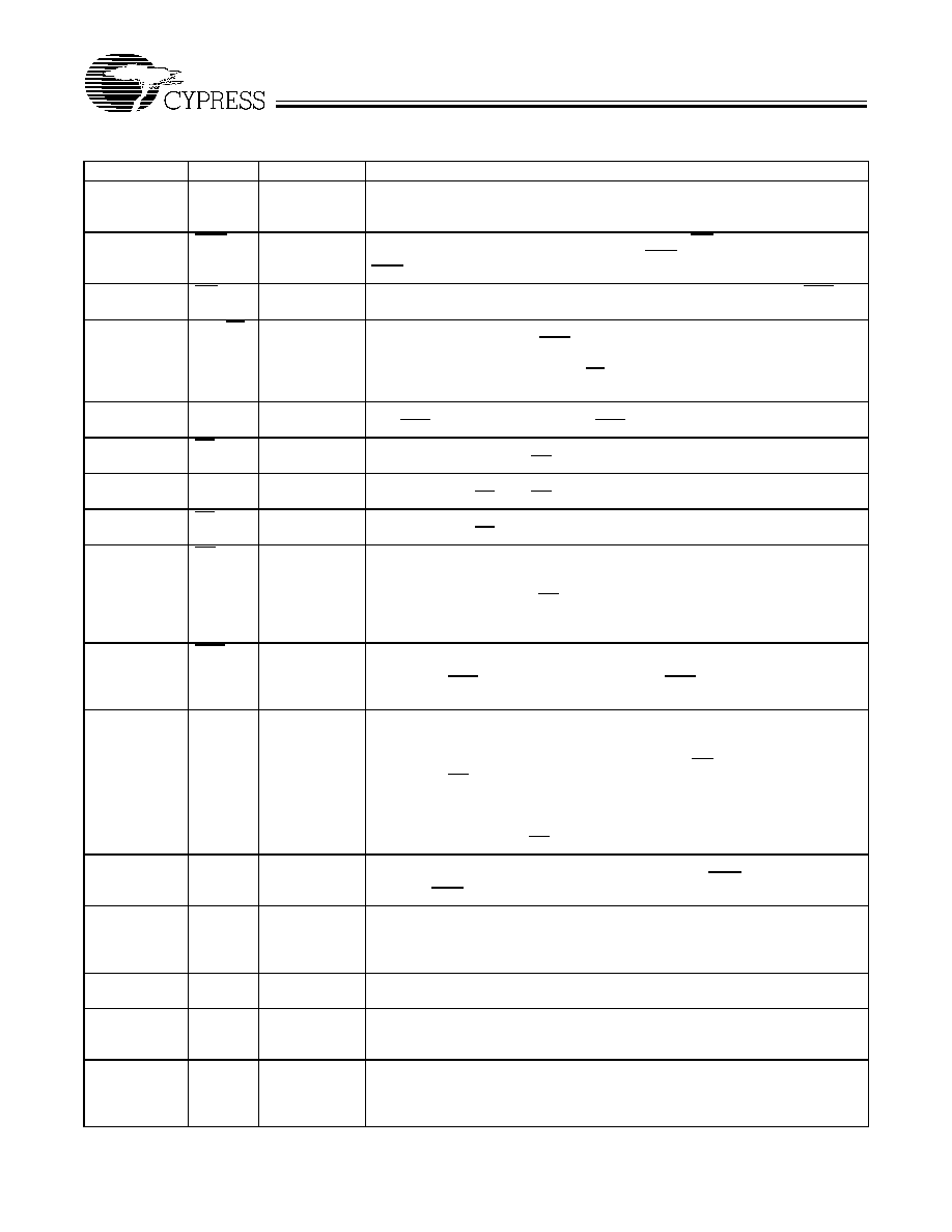
Pin Definitions
Pin Number
Name
I/O
Description
80, 50
-
44,
81
-
82, 99
-
100, 32
-
37
A
[17:0]
Input-
Synchronous
Address Inputs used to select one of the 262,144 address locations. Sampled at
the rising edge of the CLK.
94, 93
BWS
[1:0]
Input-
Synchronous
Byte Write Select Inputs, active LOW. Qualified with WE to conduct writes to the
SRAM. Sampled on the rising edge of CLK. BWS
0
controls DQ
[7:0]
and DP
0
,
BWS
1
controls DQ
[15:8]
and DP
1
. See Write Cycle Description table for details.
88
WE
Input-
Synchronous
Write Enable Input, active LOW. Sampled on the rising edge of CLK if CEN is
active LOW. This signal must be asserted LOW to initiate a write sequence.
85
ADV/LD
Input-
Synchronous
Advance/Load input used to advance the on-chip address counter or load a new
address. When HIGH (and CEN is asserted LOW) the internal burst counter is
advanced. When LOW, a new address can be loaded into the device for an ac-
cess. After being deselected, ADV/LD should be driven LOW in order to load a
new address.
89
CLK
Input-Clock
Clock input. Used to capture all synchronous inputs to the device. CLK is qualified
with CEN. CLK is only recognized if CEN is active LOW.
98
CE
1
Input-
Synchronous
Chip Enable 1 Input active LOW. Sampled on the rising edge of CLK. Used in
conjunction with CE
2
and CE
3
to select/deselect the device.
97
CE
2
Input-
Synchronous
Chip Enable 2 Input active HIGH. Sampled on the rising edge of CLK. Used in
conjunction with CE
1
and CE
3
to select/deselect the device.
92
CE
3
Input-
Synchronous
Chip Enable 3 Input, active LOW. Sampled on the rising edge of CLK. Used in
conjunction with CE
1
and
CE
2
to select/deselect the device.
86
OE
Input-
Asynchronous
Output Enable, active LOW. Combined with the synchronous logic block inside
the device to control the direction of the I/O pins. When LOW, the I/O pins are
allowed to behave as outputs. When deasserted HIGH, I/O pins are three-stated,
and act as input data pins. OE is masked during the data portion of a write
sequence, during the first clock when emerging from a deselected state, when
the device has been deselected.
87
CEN
Input-
Synchronous
Clock Enable Input, active LOW. When asserted LOW the clock signal is recog-
nized by the SRAM. When deasserted HIGH the Clock signal is masked. Since
deasserting CEN does not deselect the device, CEN can be used to extend the
previous cycle when required.
23
-
22, 19
-
18,
13
-
12, 9
-
8,
73
-
72, 69
-
68,
63
-
62, 59
-
58
DQ
[15:0]
I/O-
Synchronous
Bidirectional Data I/O lines. As inputs, they feed into an on-chip data register that
is triggered by the rising edge of CLK. As outputs, they deliver the data contained
in the memory location specified by A
[16:0]
during the previous clock rise of the
read cycle. The direction of the pins is controlled by OE and the internal control
logic. When OE is asserted LOW, the pins can behave as outputs. When HIGH,
DQ
[15:0]
are placed in a three-state condition. The outputs are automatically
three-stated during the data portion of a write sequence, during the first clock
when emerging from a deselected state, and when the device is deselected,
regardless of the state of OE.
24, 74
DP
[1:0]
I/O-
Synchronous
Bidirectional Data Parity I/O lines. Functionally, these signals are identical to
DQ
[15:0]
. During write sequences, DP
0
is controlled by BWS
0
and DP
1
is con-
trolled by BWS
1
31
MODE
Input
Strap pin
Mode input. Selects the burst order of the device. Tied HIGH selects the inter-
leaved burst order. Pulled LOW selects the linear burst order. MODE should not
change states during operation. When left floating, MODE will default HIGH to an
interleaved burst order.
15, 16, 41, 65,
66, 91
V
DD
Power Supply
Power supply inputs to the core of the device. Should be connected to 3.3V power
supply.
4, 11, 14, 20,
27, 54, 61, 70,
77
V
DDQ
I/O Power
Supply
Power supply for the I/O circuitry. Should be connected to a 3.3V power supply.
5, 10, 17, 21,
26, 40, 55, 60,
64, 67, 71, 76,
90
V
SS
Ground
Ground for the device. Should be connected to ground of the system.
CY7C1352
4
Introduction
Functional Overview
The CY7C1352 is a synchronous-pipelined Burst SRAM de-
signed specifically to eliminate wait states during Write-Read
transitions. All synchronous inputs pass through input regis-
ters controlled by the rising edge of the clock. The clock signal
is qualified with the Clock Enable input signal (CEN). If CEN is
HIGH, the clock signal is not recognized and all internal states
are maintained. All synchronous operations are qualified with
CEN. All data outputs pass through output registers controlled
by the rising edge of the clock. Maximum access delay from
the clock rise (t
CO
) is 4.0 ns (143-MHz device).
Accesses can be initiated by asserting all three chip enables
(CE
1
, CE
2
, CE
3
) active at the rising edge of the clock. If Clock
Enable (CEN) is active LOW and ADV/LD is asserted LOW, the
address presented to the device will be latched. The access
can either be a read or write operation, depending on the sta-
tus of the Write Enable (WE). BWS
[1:0]
can be used to conduct
byte write operations.
Write operations are qualified by the Write Enable (WE). All
writes are simplified with on-chip synchronous self-timed write
circuitry.
Three synchronous Chip Enables (CE
1
, CE
2
, CE
3
) and an
asynchronous Output Enable (OE) simplify depth expansion.
All operations (Reads, Writes, and Deselects) are pipelined.
ADV/LD should be driven LOW once the device has been de-
selected in order to load a new address for the next operation.
Single Read Accesses
A read access is initiated when the following conditions are
satisfied at clock rise: (1) CEN is asserted LOW, (2) CE
1
, CE
2
,
and CE
3
are ALL asserted active, (3) the Write Enable input
signal WE is deasserted HIGH, and (4) ADV/LD is asserted
LOW. The address presented to the address inputs (A
0
-
A
17
)
is latched into the Address Register and presented to the
memory core and control logic. The control logic determines
that a read access is in progress and allows the requested
data to propagate to the input of the output register. At the
rising edge of the next clock the requested data is allowed to
propagate through the output register and onto the data bus
within 4.0 ns (143-MHz device) provided OE is active LOW.
After the first clock of the read access the output buffers are
controlled by OE and the internal control logic. OE must be
driven LOW in order for the device to drive out the requested
data. During the second clock, a subsequent operation
(Read/Write/Deselect) can be initiated. Deselecting the device
is also pipelined. Therefore, when the SRAM is deselected at
clock rise by one of the chip enable signals, its output will
three-state following the next clock rise.
Burst Read Accesses
The CY7C1352 has an on-chip burst counter that allows the
user the ability to supply a single address and conduct up to
four Reads without reasserting the address inputs. ADV/LD
must be driven LOW in order to load a new address into the
SRAM, as described in the Single Read Access section above.
The sequence of the burst counter is determined by the MODE
input signal. A LOW input on MODE selects a linear burst
mode, a HIGH selects an interleaved burst sequence. Both
burst counters use A0 and A1 in the burst sequence, and will
wrap-around when incremented sufficiently. A HIGH input on
ADV/LD will increment the internal burst counter regardless of
the state of chip enables inputs or WE. WE is latched at the
beginning of a burst cycle. Therefore, the type of access (Read
or Write) is maintained throughout the burst sequence.
Single Write Accesses
Write accesses are initiated when the following conditions are
satisfied at clock rise: (1) CEN is asserted LOW, (2) CE
1
, CE
2
,
and CE
3
are ALL asserted active, and (3) the write signal WE
is asserted LOW. The address presented to A
0
-
A
17
is loaded
into the Address Register. The write signals are latched into
the Control Logic block.
On the subsequent clock rise the data lines are automatically
three-stated regardless of the state of the OE input signal. This
allows the external logic to present the data on DQ
[15:0]
and
DP
[1:0]
. In addition, the address for the subsequent access
(Read/Write/Deselect) is latched into the Address Register
(provided the appropriate control signals are asserted).
On the next clock rise the data presented to DQ
[15:0]
and
DP
[1:0]
(or a subset for byte write operations, see Write Cycle
Description table for details) inputs is latched into the device
and the write is complete.
The data written during the Write operation is controlled by
BWS
[1:0]
signals. The CY7C1352 provides byte write capabil-
ity that is described in the write cycle description table. Assert-
ing the Write Enable input (WE) with the selected Byte Write
Select (BWS
[1:0]
) input will selectively write to only the desired
bytes. Bytes not selected during a byte write operation will
remain unaltered. A synchronous self-timed write mechanism
has been provided to simplify the write operations. Byte write
capability has been included in order to greatly simplify
Read/Modify/Write sequences, which can be reduced to sim-
ple byte write operations.
Because the CY7C1352 is a common I/O device, data should
not be driven into the device while the outputs are active. The
Output Enable (OE) can be deasserted HIGH before present-
ing data to the DQ
[15:0]
and DP
[1:0]
inputs. Doing so will
three-state the output drivers. As a safety precaution, DQ
[15:0]
and DP
[1:0]
are automatically three-stated during the data por-
tion of a write cycle, regardless of the state of OE.
1
-
3, 6
-
7, 25,
28
-
30, 51
-
53,
56
-
57, 75,
78
-
79, 95
-
96
NC
-
No Connects. These pins are not connected to the internal device.
83, 84
NC
-
No Connects. Reserved for address inputs for depth expansion. Pin 83 is re-
served for 512K depth and pin 84 is reserved for 1-Mb depth devices.
38, 39, 42, 43
DNU
-
Do Not Use pins. These pins should be left floating or tied to V
SS
.
Pin Definitions
(continued)
Pin Number
Name
I/O
Description
CY7C1352
5
Burst Write Accesses
The CY7C1352 has an on-chip burst counter that allows the
user the ability to supply a single address and conduct up to
four Write operations without reasserting the address inputs.
ADV/LD must be driven LOW in order to load the initial ad-
dress, as described in the Single Write Access section above.
When ADV/LD is driven HIGH on the subsequent clock rise,
the chip enables (CE
1
, CE
2
, and CE
3
) and WE inputs are ig-
nored and the burst counter is incremented. The correct
BWS
[1:0]
inputs must be driven in each cycle of the burst write
in order to write the correct bytes of data.
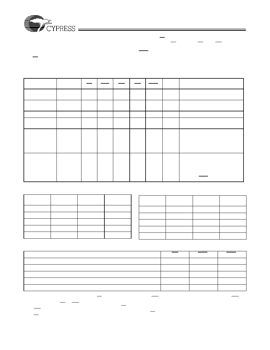
Cycle Description Truth Table
[
1, 2, 3, 4, 5, 6
]
Operation
Address
used
CE
CEN
ADV/
LD/
WE
BWS
x
CLK
Comments
Deselected
External
1
0
L
X
X
L-H
I/Os three-state following next rec-
ognized clock.
Suspend
-
X
1
X
X
X
L-H
Clock ignored, all operations
suspended.
Begin Read
External
0
0
0
1
X
L-H
Address latched.
Begin Write
External
0
0
0
0
Valid
L-H
Address latched, data presented
two valid clocks later.
Burst READ
Operation
Internal
X
0
1
X
X
L-H
Burst Read operation. Previous
access was a Read operation. Ad-
dresses incremented internally in
conjunction with the state of
MODE.
Burst WRITE
Operation
Internal
X
0
1
X
Valid
L-H
Burst Write operation. Previous
access was a Write operation. Ad-
dresses incremented internally in
conjunction with the state of
MODE. Bytes written are deter-
mined by BWS
[1:0]
.
Interleaved Burst Sequence
First
Address
Second
Address
Third
Address
Fourth
Address
Ax+1, Ax
Ax+1, Ax
Ax+1, Ax
Ax+1, Ax
00
01
10
11
01
00
11
10
10
11
00
01
11
10
01
00
Linear Burst Sequence
First
Address
Second
Address
Third
Address
Fourth
Address
Ax+1, Ax
Ax+1, Ax
Ax+1, Ax
Ax+1, Ax
00
01
10
11
01
10
11
00
10
11
00
01
11
00
01
10
Write Cycle Descriptions
[1, 2]
Function
WE
BWS
1
BWS
0
Read
1
X
X
Write
-
No bytes written
0
1
1
Write Byte 0
-
(DQ
[7:0]
and
DP
0
)
0
1
0
Write Byte 1
-
(DQ
[15:8]
and
DP
1
)
0
0
1
Write All Bytes
0
0
0
Notes:
1.
X="Don't Care", 1=Logic HIGH, 0=Logic LOW, CE stands for ALL Chip Enables active. BWSx = 0 signifies at least one Byte Write Select is active, BWSx =
Valid signifies that the desired byte write selects are asserted, see Write Cycle Description table for details.
2.
Write is defined by WE and BWS[1:0]. See Write Cycle Description table for details.
3.
The DQ and DP pins are controlled by the current cycle and the OE signal.
4.
CEN=1 inserts wait states.
5.
Device will power-up deselected and the I/Os in a three-state condition, regardless of OE.
6.
OE assumed LOW.