Cypress Semiconductor Corporation
∑
3901 North First Street
∑
San Jose
∑
CA 95134
∑
408-943-2600
Document #: 38-05198 Rev. **
Revised February 4, 2002
512K x 36/1M x 18 Flow-Thru SRAM with NoBLTM Architecture
CY7C1371B
CY7C1373B
73B
Features
∑ Pin compatible and functionally equivalent to ZBT
devices
∑ Supports 117-MHz bus operations with zero wait states
-- Data is transferred on every clock
∑ Internally self-timed output buffer control to eliminate
the need to use asynchronous OE
∑ Registered inputs for flow-thru operation
∑ Byte Write capability
∑ Common I/O architecture
∑ Fast clock-to-output times
-- 7.5 ns (for 117-MHz device)
-- 8.5 ns (for 100-MHz device)
-- 10.0ns (for 83-MHz device)
∑ Single 3.3V ≠5% and +10% power supply V
DD
∑ Separate V
DDQ
for 3.3V or 2.5V I/O
∑ Clock enable (CEN) pin to suspend operation
∑ Synchronous self-timed writes
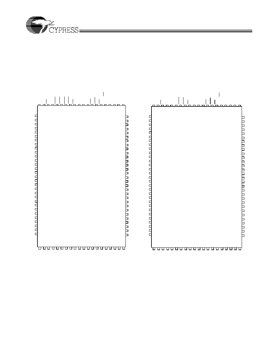
∑ Available in 100 TQFP and 119 BGA packages
∑ Burst capability ≠ linear or interleaved burst order
∑ JTAG boundary scan for BGA packaging version
∑ Automatic power down available using ZZ mode or CE
deselect
Functional Description
The CY7C1371B/CY7C1373B is 3.3V, 512K ◊ 36 and 1M ◊ 18
synchronous flow-thru burst SRAMs, respectively designed to
support unlimited true back-to-back Read/Write operations
without the insertion of wait states. The CY7C1371B/
CY7C1373B is equipped with the advanced No Bus LatencyTM
(NoBL
) logic required to enable consecutive Read/Write
operations with data being transferred on every clock cycle.
This feature dramatically improves the throughput of data
through the SRAM, especially in systems that require frequent
Write/Read transitions.The CY7C1371B/CY7C1373B is pin
compatible and functionally equivalent to ZBT devices.
All synchronous inputs pass through input registers controlled
by the rising edge of the clock.The clock input is qualified by
the Clock enable (CEN) signal, which when deasserted
suspends operation and extends the previous clock cycle.
Maximum access delay from the clock rise is 7.5 ns (117-MHz
device).
Write operations are controlled by the byte Write Selects
(BWS
a,b,c,d
for CY7C1371B and BWS
a,b
for CY7C1373B) and
a Write enable (WE) input. All writes are conducted with
on-chip synchronous self-timed Write circuitry. ZZ may be tied
to LOW if it is not used.
Synchronous Chip enables (CE
1
, CE
2
, CE
3
on the TQFP, CE
1
on the BGA) and an asynchronous Output enable (OE)
provide for easy bank selection and output three-state control.
In order to avoid bus contention, the output drivers are
synchronously three-stated during the data portion of a Write
sequence.
CLK
A
x
CEN
WE
BWS
x
CE1
CE
CE2
OE
256K X 36/
Memory
Array
Logic Block Diagram
DQ
x
Data-In REG.
Q
D
CE
Control
and Write
Logic
3
ADV/LD
Mode
DP
x
CY7C1371
CY7C1373
AX
DQX
DPX
BWSX
512K X 18
X = 18:0
X = 19:0
X= a, b, c, d X = a, b
X = a, b
X = a, b
X = a, b, c, d
X = a, b, c, d
Selection Guide
117 MHz
100 MHz
83 MHz
Unit
Maximum Access Time
7.5
8.5
10.0
ns
Maximum Operating Current
250
225
185
mA
Maximum CMOS Standby Current
20
20
20
mA
CY7C1371B
CY7C1373B
Document #: 38-05198 Rev. **
Page 5 of 26
Pin Definitions
Name
I/O Type
Description
A0
A1
A
Input-
Synchronous
Address inputs used to select one of the 532,288/1,048,576 address locations. Sampled
at the rising edge of the CLK.
BWSa
BWSb
BWSc
BWSd
Input-
Synchronous
Byte Write Select inputs, active LOW. Qualified with WE to conduct Writes to the SRAM.
Sampled on the rising edge of CLK. BWSa controls DQa
and DPa, BWSb controls DQb
and
DPb, BWSc controls DQc
and DPc, BWSd controls DQd
and DPd.
WE
Input-
Synchronous
Write enable input, active LOW. Sampled on the rising edge of CLK if CEN is active LOW.
This signal must be asserted LOW to initiate a Write sequence.
ADV/LD
Input-
Synchronous
Advance/Load input used to advance the on-chip address counter or load a new address.
When HIGH (and CEN is asserted LOW) the internal burst counter is advanced. When LOW,
a new address can be loaded into the device for an access. After being deselected, ADV/LD
should be driven LOW in order to load a new address.
CLK
Input-Clock
Clock input. Used to capture all synchronous inputs to the device. CLK is qualified with CEN.
CLK is only recognized if CEN is active LOW.
CE
1
Input-
Synchronous
Chip enable 1 input, active LOW. Sampled on the rising edge of CLK. Used in conjunction
with CE
2
and CE
3
to select/deselect the device.
CE
2
Input-
Synchronous
Chip enable 2 input, active HIGH. Sampled on the rising edge of CLK. Used in conjunction
with CE
1
and CE
3
to select/deselect the device.
CE
3
Input-
Synchronous
Chip enable 3 input, active LOW. Sampled on the rising edge of CLK. Used in conjunction
with CE
1
and
CE
2
to select/deselect the device.
OE
Input-
Asynchronous
Output enable, active LOW. Combined with the synchronous logic block inside the device
to control the direction of the I/O pins. When LOW, the I/O pins are allowed to behave as
outputs. When deasserted HIGH, I/O pins are three-stated, and act as input data pins. OE is
masked during the data portion of a Write sequence, during the first clock when emerging
from a deselected state and when the device has been deselected.
CEN
Input-
Synchronous
Clock enable input, active LOW. When asserted LOW the clock signal is recognized by the
SRAM. When deasserted HIGH the clock signal is masked. Since deasserting CEN does not
deselect the device, CEN can be used to extend the previous cycle when required.
DQa
DQb
DQc
DQd
I/O-
Synchronous
Bidirectional Data I/O lines. As inputs, they feed into an on-chip data register that is
triggered by the rising edge of CLK. As outputs, they deliver the data contained in the memory
location specified by A
[X]
during the previous clock rise of the Read cycle. The direction of
the pins is controlled by OE and the internal control logic. When OE is asserted LOW, the
pins can behave as outputs. When HIGH, DQa ≠ DQd are placed in a three-state condition.
The outputs are automatically three-stated during the data portion of a Write sequence, during
the first clock when emerging from a deselected state, and when the device is deselected,
regardless of the state of OE. DQ a, b, c and d are eight-bits wide.
DPa
DPb
DPc
DPd
I/O-
Synchronous
Bidirectional Data Parity I/O lines. Functionally, these signals are identical to DQ
[31:0]
.
During Write sequences, DPa is controlled by BWSa, DPb is controlled by BWSb, DPc is
controlled by BWSc, and DPd is controlled by BWSd. DP a, b, c and d are one-bit wide.
ZZ
Input-
Asynchronous
ZZ "sleep" input. This active HIGH input places the device in a non-time critical "sleep"
condition with data integrity preserved.
MODE
Input Pin
Mode input. Selects the burst order of the device. Tied HIGH selects the interleaved burst
order. Pulled LOW selects the linear burst order. MODE should not change states during
operation. When left floating MODE will default HIGH, to an interleaved burst order.
V
DD
Power Supply
Power supply inputs to the core of the device.
V
DDQ
I/O Power
Supply
Power supply for the I/O circuitry.
V
SS
Ground
Ground for the device. Should be connected to ground of the system.
TDO
JTAG serial output
Synchronous
Serial data-out to the JTAG circuit. Delivers data on the negative edge of TCK (BGA only).