 | ÐлекÑÑоннÑй компоненÑ: CY7C145 | СкаÑаÑÑ:  PDF PDF  ZIP ZIP |
/home/web/htmldatasheet/RUSSIAN/html/cypress/169530
8K x 8/9 Dual-Port Static RAM
with Sem, Int, Busy
fax id: 5205
CY7C145
CY7C144
Cypress Semiconductor Corporation
·
3901 North First Street
·
San Jose
·
CA 95134
·
408-943-2600
November 1996
1CY 7C14 4
Features
· True Dual-Ported memory cells which allow
simultaneous reads of the same memory location
· 8K x 8 organization (CY7C144)
· 8K x 9 organization (CY7C145)
· 0.65-micron CMOS for optimum speed/power
· High-speed access: 15ns
· Low operating power: I
CC
= 160 mA (max.)
· Fully asynchronous operation
· Automatic power-down
· TTL compatible
· Master/Slave select pin allows bus width expansion to
16/18 bits or more
· Busy arbitration scheme provided
· Semaphores included to permit software handshaking
between ports
· INT flag for port-to-port communication
· Available in 68-pin PLCC, 64-pin and 80-pin TQFP
· Pin compatible and functionally equivalent to
IDT7005/IDT7015
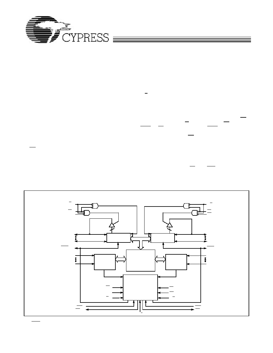
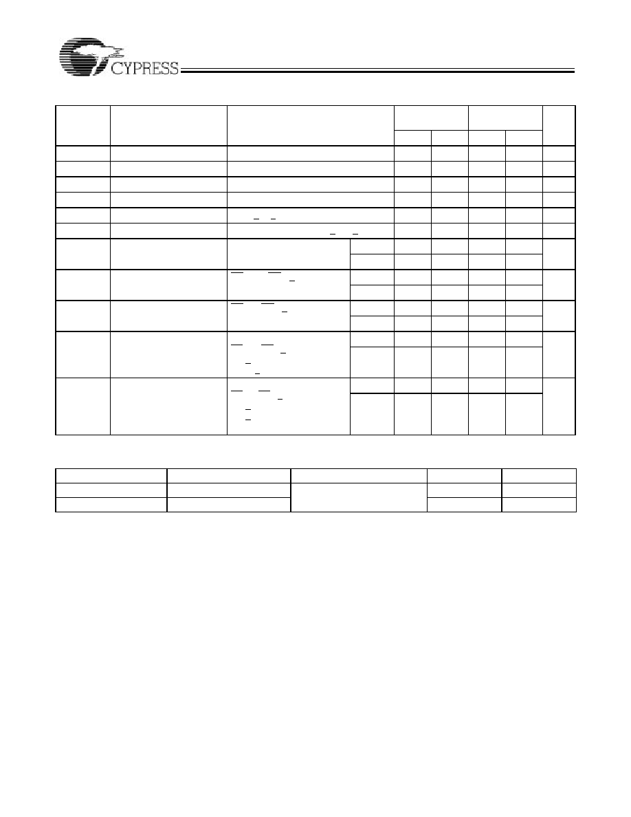
Functional Description
The CY7C144 and CY7C145 are high-speed CMOS 8K x 8
and 8K x 9 dual-port static RAMs. Various arbitration schemes
are included on the CY7C144/5 to handle situations when mul-
tiple processors access the same piece of data. Two ports are
provided permitting independent, asynchronous access for
reads and writes to any location in memory. The CY7C144/5
can be utilized as a standalone 64/72-Kbit dual-port static
RAM or multiple devices can be combined in order to function
as a 16/18-bit or wider master/slave dual-port static RAM. An
M/S pin is provided for implementing 16/18-bit or wider mem-
ory applications without the need for separate master and
slave devices or additional discrete logic. Application areas
include interprocessor/multiprocessor designs, communica-
tions status buffering, and dual-port video/graphics memory.
Each port has independent control pins: chip enable (CE),
read or write enable (R/W), and output enable (OE). Two flags,
BUSY and INT, are provided on each port. BUSY signals that the port
is trying to access the same location currently being accessed by the
other port. The interrupt flag (INT) permits communication between
ports or systems by means of a mail box. The semaphores are used
to pass a flag, or token, from one port to the other to indicate that a
shared resource is in use. The semaphore logic is comprised of eight
shared latches. Only one side can control the latch (semaphore) at
any time. Control of a semaphore indicates that a shared resource is
in use. An automatic power-down feature is controlled independently
on each port by a chip enable (CE) pin or SEM pin.
Notes:
1.
BUSY is an output in master mode and an input in slave mode.
2.
Interrupt: push-pull output and requires no pull-up resistor.
C144-1
R/W
L
CE
L
OE
L
A
12L
A
0L
A
0R
A
12R
R/W
R
CE
R
OE
R
CE
R
OE
R
CE
L
OE
L
R/W
L
R/W
R
I/O
7L
I/O
0L
I/O
7R
I/O
0R
INTERRUPT
SEMAPHORE
ARBITRATION
CONTROL
I/O
CONTROL
I/O
MEMORY
ARRAY
ADDRESS
DECODER
ADDRESS
DECODER
SEM
L
SEM
R
BUSY
L
BUSY
R
INT
L
INT
R
M/S
(7C145) I/O
8L
I/O
8R
(7C145)
Logic Block Diagram
[1, 2]
[1, 2]
[2]
[2]
CY7C145
CY7C144
2
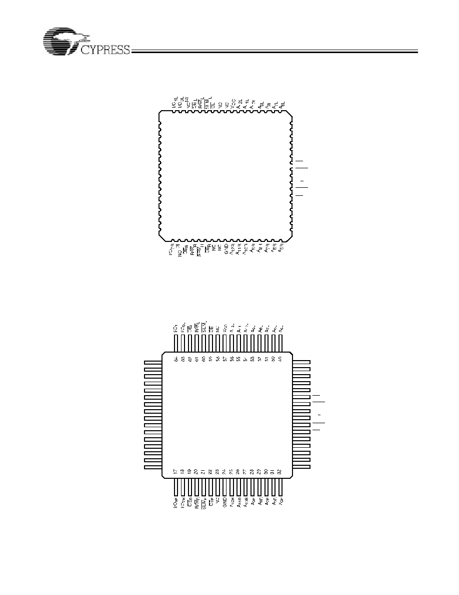
Pin Configurations
Notes:
3.
I/O
8R
on the CY7C145.
4.
I/O
8L
on the CY7C145.
64-Pin TQFP
Top View
1
2
3
4
5
6
7
8
9
10
11
12
13
14
15
48
47
46
45
44
43
42
41
40
39
38
37
36
35
34
33
16
I/O
2L
I/O
3L
I/O
4L
I/O
5L
I/O
6L
I/O
7L
V
CC
GND
I/O
0R
I/O
1R
I/O
2R
I/O
3R
I/O
4R
I/O
5R
GND
V
CC
A
4L
A
3L
A
2L
A
1L
A
0L
GND
BUSY
L
BUSY
R
M/S
A
0R
A
1R
A
2R
A
3R
A
4R
INT
L
INT
R
CY7C144
10
11
12
13
14
15
16
17
18
19
20
21
22
23
24
67
Top View
68-Pin PLCC
60
59
58
57
56
55
54
53
52
51
50
49
48
3132 33 34 35 36 37 38 39 40 41 42 43
5 4 3 2 1 68
66 65 64 63 62 61
A
4L
A
3L
A
2L
A
1L
A
0L
INT
L
BUSY
L
GND
M/S
BUSY
R
INT
R
A
0R
I/O
2L
I/O
3L
I/O
4L
I/O
5L
GND
I/O
6L
I/O
7L
V
CC
GND
I/O
0R
I/O
1R
I/O
2R
V
CC
2728 29 30
9 8 7 6
47
46
45
44
A
1R
A
2R
A
3R
A
4R
I/O
3R
I/O
4R
I/O
5R
I/O
6R
25
26
A
5L
C144-2
C144-3
CY7C144/5
CY7C145
CY7C144
3
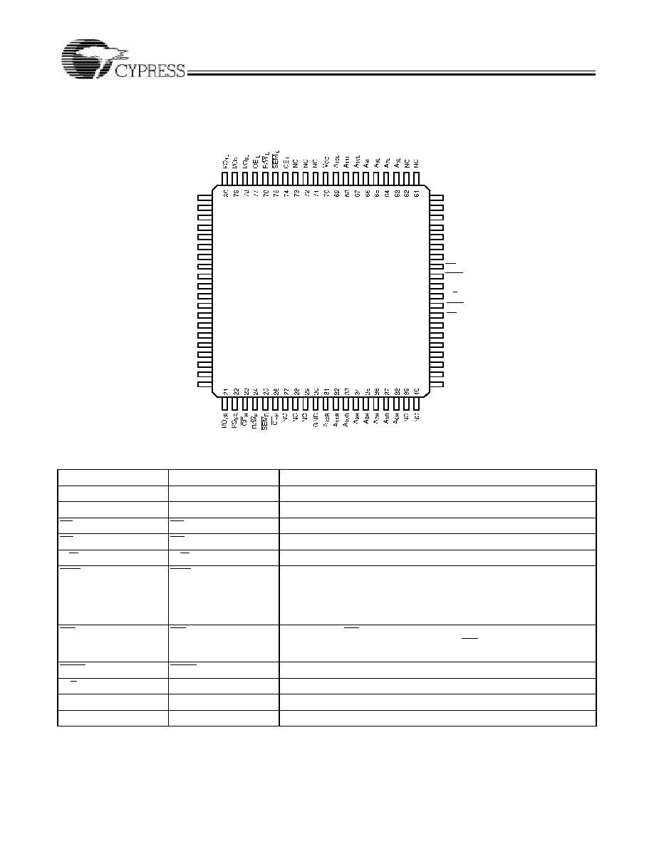
Pin Configurations (continued)
1
2
3
4
5
6
7
8
9
10
11
12
13
14
15
17
16
18
19
20
60
59
58
57
56
55
54
53
52
51
50
49
48
47
46
44
45
43
42
41
80-Pin TQFP
Top View
I/O
2L
I/O
3L
I/O
4L
I/O
5L
I/O
6L
I/O
7L
V
CC
GND
I/O
0R
I/O
1R
2R
I/O
3R
I/O
4R
5R
GND
V
CC
A
5L
A
4L
A
3L
A
2L
A
1L
A
0L
GND
BUSY
L
M/S
A
0R
A
1R
A
2R
A
3R
A
4R
INT
L
I/O
6R
CY7C145
BUSY
R
INT
R
NC
NC
NC
C144-4
NC
NC
I/O
I/O
NC
Pin Definitions
Left Port
Right Port
Description
I/O
0L
-
7L(8L)
I/O
0R
-
7R(8R)
Data bus Input/Output
A
0L
-
12L
A
0R
-
12R
Address Lines
CE
L
CE
R
Chip Enable
OE
L
OE
R
Output Enable
R/W
L
R/W
R
Read/Write Enable
SEM
L
SEM
R
Semaphore Enable. When asserted LOW, allows access to eight sema-
phores. The three least significant bits of the address lines will determine
which semaphore to write or read. The I/O
0
pin is used when writing to a
semaphore. Semaphores are requested by writing a 0 into the respective
location.
INT
L
INT
R
Interrupt Flag. INT
L
is set when right port writes location 1FFE and is
cleared when left port reads location 1FFE. INT
R
is set when left port writes
location 1FFF and is cleared when right port reads location 1FFF.
BUSY
L
BUSY
R
Busy Flag
M/S
Master or Slave Select
V
CC
Power
GND
Ground
CY7C145
CY7C144
4
Maximum Ratings
(Above which the useful life may be impaired. For user guide-
lines, not tested.)
Storage Temperature
..................................... -
65
°
C to +150
°
C
Ambient Temperature with
Power Applied
.................................................. -
55
°
C to +125
°
C
Supply Voltage to Ground Potential
.................-
0.5V to +7.0V
DC Voltage Applied to Outputs
in High Z State
.....................................................-
0.5V to +7.0V
DC Input Voltage
[5]
..............................................-
0.5V to +7.0V
Output Current into Outputs (LOW)............................. 20 mA
Static Discharge Voltage .......................................... >2001V
(per MIL-STD-883, Method 3015)
Latch-Up Current .................................................... >200 mA
Selection Guide
7C144-15
7C145-15
7C144-25
7C145-25
7C144-35
7C145-35
7C144-55
7C145-55
Maximum Access Time (ns)
15
25
35
55
Maximum Operating
Current (mA)
220
180
160
160
Maximum Standby
Current for I
SB1
(mA)
60
40
30
30
Operating Range
Range
Ambient
Temperature
V
CC
Commercial
0
°
C to +70
°
C
5V
±
10%
Industrial
-
40
°
C to +85
°
C
5V
±
10%
Electrical Characteristics
Over the Operating Range
Parameter
Description
Test Conditions
7C144-15
7C145-15
7C144-25
7C145-25
Unit
Min.
Max.
Min.
Max.
V
OH
Output HIGH Voltage
V
CC
= Min., I
OH
=
-
4.0 mA
2.4
2.4
V
V
OL
Output LOW Voltage
V
CC
= Min., I
OL
= 4.0 mA
0.4
0.4
V
V
IH
Input HIGH Voltage
2.2
2.2
V
V
IL
Input LOW Voltage
0.8
0.8
V
I
IX
Input Leakage Current
GND < V
I
< V
CC
-
10
+10
-
10
+10
µ
A
I
OZ
Output Leakage Current
Outputs Disabled, GND < V
O
< V
CC
-
10
+10
-
10
+10
µ
A
I
CC
Operating Current
V
CC
= Max., I
OUT
= 0 mA
Outputs Disabled
Com'l
220
180
mA
Ind
190
I
SB1
Standby Current
(Both Ports TTL Levels)
CE
L
and CE
R
> V
IH
,
f = f
MAX
[7]
Com'l
60
40
mA
Ind
50
I
SB2
Standby Current
(One Port TTL Level)
CE
L
or CE
R
> V
IH
,
f = f
MAX
[7]
Com'l
130
110
mA
Ind
120
I
SB3
Standby Current
(Both Ports CMOS Levels)
Both Ports
CE and CE
R
> V
CC
0.2V,
V
IN
> V
CC
0.2V
or V
IN
< 0.2V, f = 0
[7]
Com'l
15
15
mA
Ind
30
I
SB4
Standby Current
(One Port CMOS Level)
One Port
CE
L
or CE
R
> V
CC
0.2V,
V
IN
> V
CC
0.2V or
V
IN
< 0.2V, Active
Port Outputs, f = f
MAX
[7]
Com'l
125
100
mA
Ind
115
Notes:
5.
Pulse width < 20 ns.
6.
T
A
is the "instant on" case temperature.
7.
f
MAX
= 1/t
RC
= All inputs cycling at f = 1/t
RC
(except output enable). f = 0 means no address or control lines change. This applies only to inputs at CMOS
level standby I
SB3
.
CY7C145
CY7C144
5
]
Electrical Characteristics
Over the Operating Range (continued)
Parameter
Description
Test Conditions
7C144-35
7C145-35
7C144-55
7C145-55
Unit
Min.
Max.
Min.
Max.
V
OH
Output HIGH Voltage
V
CC
= Min., I
OH
=
-
4.0 mA
2.4
2.4
V
V
OL
Output LOW Voltage
V
CC
= Min., I
OL
= 4.0 mA
0.4
0.4
V
V
IH
Input HIGH Voltage
2.2
2.2
V
V
IL
Input LOW Voltage
0.8
0.8
V
I
IX
Input Leakage Current
GND < V
I
< V
CC
-
10
+10
-
10
+10
µ
A
I
OZ
Output Leakage Current
Outputs Disabled, GND < V
O
< V
CC
-
10
+10
-
10
+10
µ
A
I
CC
Operating Current
V
CC
= Max., I
OUT
= 0 mA
Outputs Disabled
Com'l
160
160
mA
Ind
180
180
I
SB1
Standby Current
(Both Ports TTL Levels)
CE
L
and CE
R
> V
IH
,
f = f
MAX
[7]
Com'l
30
30
mA
Ind
40
40
I
SB2
Standby Current
(One Port TTL Level)
CE
L
or CE
R
> V
IH
,
f = f
MAX
[7]
Com'l
100
100
mA
Ind
110
110
I
SB3
Standby Current
(Both Ports CMOS Levels)
Both Ports
CE and CE
R
> V
CC
0.2V,
V
IN
> V
CC
0.2V
or V
IN
< 0.2V, f = 0
[7]
Com'l
15
15
mA
Ind
30
30
I
SB4
Standby Current
(One Port CMOS Level)
One Port
CE
L
or CE
R
> V
CC
0.2V,
V
IN
> V
CC
0.2V or
V
IN
< 0.2V, Active
Port Outputs, f = f
MAX
[7]
Com'l
90
90
mA
Ind
100
100
Capacitance
[8]
Parameter
Description
Test Conditions
Max.
Unit
C
IN
Input Capacitance
T
A
= 25
°
C, f = 1 MHz,
V
CC
= 5.0V
10
pF
C
OUT
Output Capacitance
15
pF
Note:
8.
Tested initially and after any design or process changes that may affect these parameters.
CY7C145
CY7C144
6
AC Test Loads and Waveforms
3.0V
GND
90%
90%
10%
3 ns
3 ns
10%
ALL INPUT PULSES
(a) Normal Load (Load1)
5V
OUTPUT
C = 30 pF
V
TH
=1.4V
OUTPUT
C=30pF
(b) Th évenin Equivalent (Load 1)
(c) Three-State Delay (Load 3)
C = 30 pF
OUTPUT
Load (Load 2)
C144-5
C144-6
C144-7
C144-8
C144-9
5V
OUTPUT
C = 5 pF
R1=893
R2=347
R
TH
=250
R1=893
R2=347
Switching Characteristics
Over the Operating Range
[9]
7C144-15
7C145-15
7C144-25
7C145-25
7C144-35
7C145-35
7C144-55
7C145-55
Parameter
Description
Min.
Max.
Min.
Max.
Min.
Max.
Min.
Max.
Unit
READ CYCLE
t
RC
Read Cycle Time
15
25
35
55
ns
t
AA
Address to Data Valid
15
25
35
55
ns
t
OHA
Output Hold From Address
Change
3
3
3
3
ns
t
ACE
CE LOW to Data Valid
15
25
35
55
ns
t
DOE
OE LOW to Data Valid
10
15
20
25
ns
t
LZOE
[10, 11,12]
OE Low to Low Z
3
3
3
3
ns
t
HZOE
[10, 11,12]
OE HIGH to High Z
10
15
20
25
ns
t
LZCE
[10, 11,12]
CE LOW to Low Z
3
3
3
3
ns
t
HZCE
[10, 11,12]
CE HIGH to High Z
10
15
20
25
ns
t
PU
[12]
CE LOW to Power-Up
0
0
0
0
ns
t
PD
[12]
CE HIGH to Power-Down
15
25
35
55
ns
Notes:
9.
Test conditions assume signal transition time of 3 ns or less, timing reference levels of 1.5V, input pulse levels of 0 to 3.0V, and output loading of the specified
I
OI
/I
OH
and 30-pF load capacitance.
10. At any given temperature and voltage condition for any given device, t
HZCE
is less than t
LZCE
and t
HZOE
is less than t
LZOE
.
11.
Test conditions used are Load 3.
12. This parameter is guaranteed but not tested.
CY7C145
CY7C144
7
WRITE CYCLE
t
WC
Write Cycle Time
15
25
35
55
ns
t
SCE
CE LOW to Write End
12
20
30
45
ns
t
AW
Address Set-Up to Write End
12
20
30
45
ns
t
HA
Address Hold From Write
End
2
2
2
2
ns
t
SA
Address Set-Up to Write
Start
0
0
0
0
ns
t
PWE
Write Pulse Width
12
20
25
40
ns
t
SD
Data Set-Up to Write End
10
15
15
25
ns
t
HD
Data Hold From Write End
0
0
0
0
ns
t
HZWE
[11,12]
R/W LOW to High Z
10
15
20
25
ns
t
LZWE
[11,12]
R/W HIGH to Low Z
3
3
3
3
ns
t
WDD
[13]
Write Pulse to Data Delay
30
50
60
70
ns
t
DDD
[13]
Write Data Valid to Read
Data Valid
25
30
35
40
ns
BUSY TIMING
[14]
t
BLA
BUSY LOW from Address
Match
15
20
20
30
ns
t
BHA
BUSY HIGH from Address
Mismatch
15
20
20
30
ns
t
BLC
BUSY LOW from CE LOW
15
20
20
30
ns
t
BHC
BUSY HIGH from CE HIGH
15
20
20
30
ns
t
PS
Port Set-Up for Priority
5
5
5
5
ns
t
WB
R/W LOW after BUSY LOW
0
0
0
0
ns
t
WH
R/W HIGH after BUSY HIGH
13
20
30
30
ns
t
BDD
BUSY HIGH to Data Valid
15
25
35
55
ns
INTERRUPT TIMING
[14]
t
INS
INT Set Time
15
25
25
35
ns
t
INR
INT Reset Time
15
25
25
35
ns
SEMAPHORE TIMING
t
SOP
SEM Flag Update Pulse (OE
or SEM)
10
10
15
20
ns
t
SWRD
SEM Flag Write to Read Time
5
5
5
5
ns
t
SPS
SEM Flag Contention
Window
5
5
5
5
ns
Notes:
13. For information on part-to-part delay through RAM cells from writing port to reading port, refer to Read Timing with Port-to-Port Delay waveform.
14. Test conditions used are Load 2.
Switching Characteristics
Over the Operating Range
[9]
(continued)
7C144-15
7C145-15
7C144-25
7C145-25
7C144-35
7C145-35
7C144-55
7C145-55
Parameter
Description
Min.
Max.
Min.
Max.
Min.
Max.
Min.
Max.
Unit
CY7C145
CY7C144
8
Switching Waveforms
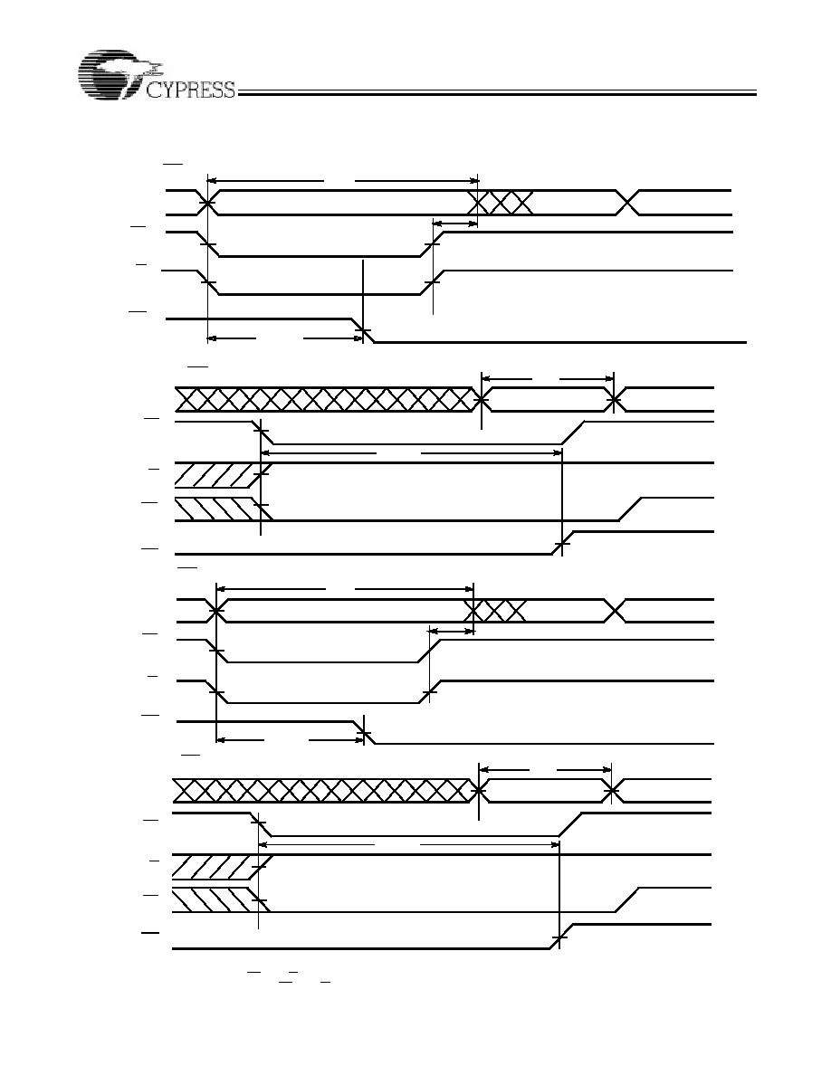
Read Cycle No. 1 (Either Port Address Access)
[15, 16]
Read Cycle No. 2 (Either Port CE/OE Access)
[15, 17, 18]
Read Timing with Port-to-Port Delay (M/S=L)
[19, 20]
Notes:
15. R/W is HIGH for read cycle.
16. Device is continuously selected CE = LOW and OE = LOW. This waveform cannot be used for semaphore reads.
17. Address valid prior to or coincident with CE transition LOW.
18. CE
L
= L, SEM = H when accessing RAM. CE = H, SEM = L when accessing semaphores.
19. BUSY = HIGH for the writing port.
20. CE
L
= CE
R
= LOW.
t
RC
t
AA
t
OHA
DATA VALID
PREVIOUS DATA VALID
DATA OUT
ADDRESS
C144-10
t
ACE
t
LZOE
t
DOE
t
HZOE
t
HZCE
DATA VALID
DATA OUT
SEM or CE
OE
t
LZCE
t
PU
I
CC
I
SB
t
PD
C144-11
VALID
t
DDD
t
WDD
MATCH
MATCH
R/W
R
DATAIN
R
DATA
OUTL
C144-12
t
WC
ADDRESS
R
t
PWE
VALID
t
SD
t
HD
ADDRESS
L
CY7C145
CY7C144
9
Write Cycle No. 1: OE Three-State Data I/Os (Either Port)
[21, 22, 23]
Write Cycle No. 2: R/W Three-State Data I/Os (Either Port)
[21, 23, 24]
Notes:
21. The internal write time of the memory is defined by the overlap of CE or SEM LOW and R/W LOW. Both signals must be LOW to initiate a write, and either
signal can terminate a write by going HIGH. The data input set-up and hold timing should be referenced to the rising edge of the signal that terminates
the write.
22. If OE is LOW during a R/W controlled write cycle, the write pulse width must be the larger of t
PWE
or (t
HZWE
+ t
SD
) to allow the I/O drivers to turn off and
data to be placed on the bus for the required t
SD
. If OE is HIGH during a R/W controlled write cycle (as in this example), this requirement does not apply
and the write pulse can be as short as the specified t
PWE
.
23. R/W must be HIGH during all address transitions.
24. Data I/O pins enter high impedance when OE is held LOW during write.
Switching Waveforms (continued)
C144-13
t
AW
t
WC
DATA VALID
HIGH IMPEDANCE
t
SCE
t
SA
t
PWE
t
HD
t
SD
t
HA
t
HZOE
t
LZOE
SEM OR CE
R/W
ADDRESS
OE
DATA OUT
DATA IN
t
AW
t
WC
t
SCE
t
SA
t
PWE
t
HD
t
SD
t
HZWE
t
HA
HIGH IMPEDANCE
SEM OR CE
R/W
ADDRESS
DATA OUT
DATA IN
t
LZWE
DATAVALID
C144-14
CY7C145
CY7C144
10
Semaphore Read After Write Timing, Either Side
[25]
Semaphore Contention
[26, 27, 28]
Notes:
25. CE = HIGH for the duration of the above timing (both write and read cycle).
26. I/O
0R
= I/O
0L
= LOW (request semaphore); CE
R
= CE
L
= HIGH
27. Semaphores are reset (available to both ports) at cycle start.
28. If t
SPS
is violated, the semaphore will definitely be obtained by one side or the other, but there is no guarantee which side will control the semaphore.
Switching Waveforms (continued)
t
SOP
t
AA
SEM
R/W
OE
I/O
0
C144-15
VALID ADDRESS
VALID ADDRESS
t
HD
DATA
IN
VALID
DATA
OUT
VALID
t
OHA
A
0
-
A
2
t
AW
t
HA
t
ACE
t
SOP
t
SCE
t
SD
t
SA
t
PWE
t
SWRD
t
DOE
WRITE CYCLE
READ CYCLE
MATCH
C144-16
t
SPS
A
0L
-
A
2L
MATCH
R/W
L
SEM
L
A
0R
-
A
2R
R/W
R
SEM
R
CY7C145
CY7C144
11
Read with BUSY (M/S=HIGH)
[20]
Write Timing with Busy Input (M/S=LOW)
Switching Waveforms (continued)
VALID
t
DDD
t
WDD
MATCH
MATCH
R/W
R
DATAIN
R
DATA
OUTL
C14417
t
WC
ADDRESS
R
t
PWE
VALID
t
SD
t
HD
ADDRESS
L
t
PS
t
BLA
t
BHA
t
BDD
BUSY
L
t
PWE
R/W
BUSY
t
WB
t
WH
C14418
CY7C145
CY7C144
12
Busy Timing Diagram No. 1 (CE Arbitration)
[29]
Busy Timing Diagram No. 2 (Address Arbitration)
[29]
Notes:
29. If t
PS
is violated, the busy signal will be asserted on one side or the other, but there is no guarantee on which side BUSY will be asserted
Switching Waveforms (continued)
ADDRESS MATCH
t
PS
t
BLC
t
BHC
ADDRESS MATCH
t
PS
t
BLC
t
BHC
CE
R
Valid First:
ADDRESS
L,R
BUSY
R
CE
L
CE
R
BUSY
L
CE
R
CE
L
ADDRESS
L,R
C144-19
C144-20
CE
L
Valid First:
ADDRESS MATCH
t
PS
ADDRESS
L
BUSY
R
ADDRESS MISMATCH
t
RC
or t
WC
t
BLA
t
BHA
ADDRESS
R
ADDRESS MATCH
ADDRESS MISMATCH
t
PS
ADDRESS
L
BUSY
L
t
RC
or t
WC
t
BLA
t
BHA
ADDRESS
R
Right Address Valid First:
C144-21
C144-22
Left Address Valid First:
CY7C145
CY7C144
13
Interrupt Timing Diagrams
Notes:
30. t
HA
depends on which enable pin (CE
L
or R/W
L
) is deasserted first.
31. t
INS
or t
INR
depends on which enable pin (CE
L
or R/W
L
) is asserted last.
Switching Waveforms (continued)
WRITE 1FFF
t
WC
t
HA
Left Side Sets INT
R
:
ADDRESS
L
R/W
L
CE
L
INT
R
t
INS
C144-23
[30]
[31]
Right Side Clears INT
R
:
READ 1FFF
t
RC
t
INR
WRITE 1FFE
t
WC
Right Side Sets INT
L
:
Left Side Clears INT
L
:
READ 1FFE
t
INR
t
RC
ADDRESS
R
CE
L
R/W
L
INT
L
OE
L
ADDRESS
R
R/W
R
CE
R
INT
L
ADDRESS
R
CE
R
R/W
R
INT
R
OE
R
t
HA
t
INS
C144-24
C144-25
C144-26
[31]
[30]
[31]
[31]

CY7C145
CY7C144
14
Architecture
The CY7C144/5 consists of a an array of 8K words of 8/9 bits
each of dual-port RAM cells, I/O and address lines, and control
signals (CE, OE, R/W). These control pins permit indepen-
dent access for reads or writes to any location in memory. To
handle simultaneous writes/reads to the same location, a
BUSY pin is provided on each port. Two interrupt (INT) pins
can be utilized for port-to-port communication. Two sema-
phore (SEM) control pins are used for allocating shared re-
sources. With the M/S pin, the CY7C144/5 can function as
a Master (BUSY pins are outputs) or as a slave (BUSY pins
are inputs). The CY7C144/5 has an automatic power-down
feature controlled by CE. Each port is provided with its own
output enable control (OE), which allows data to be read
from the device.
Functional Description
Write Operation
Data must be set up for a duration of t
SD
before the rising
edge of R/W in order to guarantee a valid write. A write op-
eration is controlled by either the OE pin (see Write Cycle
No.1 waveform) or the R/W pin (see Write Cycle No. 2 wave-
form). Data can be written to the device t
HZOE
after the OE
is deasserted or t
HZWE
after the falling edge of R/W. Re-
quired inputs for non-contention operations are summarized
in
Table 1.
If a location is being written to by one port and the opposite
port attempts to read that location, a port-to-port flowthrough
delay must be met before the data is read on the output; oth-
erwise the data read is not deterministic. Data will be valid on
the port t
DDD
after the data is presented on the other port.
Read Operation
When reading the device, the user must assert both the OE
and CE pins. Data will be available t
ACE
after CE or t
DOE
after
OE are asserted. If the user of the CY7C144/5 wishes to ac-
cess a semaphore flag, then the SEM pin must be asserted
instead of the CE pin.
Interrupts
The interrupt flag (INT) permits communications between
ports.When the left port writes to location 1FFF, the right port's inter-
rupt flag (INT
R
) is set. This flag is cleared when the right port reads
that same location. Setting the left port's interrupt flag (INT
L
) is accom-
plished when the right port writes to location 1FFE. This flag is cleared
when the left port reads location 1FFE. The message at 1FFF or
1FFE is user-defined. See
Table 2 for input requirements for INT.
INT
R
and INT
L
are push-pull outputs and do not require pull-up resis-
tors to operate.
Busy
The CY7C144/5 provides on-chip arbitration to alleviate simul-
taneous memory location access (contention). If both ports'
CEs are asserted and an address match occurs within t
PS
of each
other the Busy logic will determine which port has access. If t
PS
is
violated, one port will definitely gain permission to the location, but it
is not guaranteed which one. BUSY will be asserted t
BLA
after an
address match or t
BLC
after CE is taken LOW. BUSY
L
and BUSY
R
in master mode are push-pull outputs and do not require pull-up re-
sistors to operate.
Master/Slave
An M/S pin is provided in order to expand the word width by config-
uring the device as either a master or a slave. The BUSY output of
the master is connected to the BUSY input of the slave. This will allow
the device to interface to a master device with no external compo-
nents.Writing of slave devices must be delayed until after the BUSY
input has settled. Otherwise, the slave chip may begin a write cycle
during a contention situation.When presented a HIGH input, the M/S
pin allows the device to be used as a master and therefore the BUSY
line is an output. BUSY can then be used to send the arbitration out-
come to a slave.
Semaphore Operation
The CY7C144/5 provides eight semaphore latches which are
separate from the dual-port memory locations. Semaphores
are used to reserve resources that are shared between the two
ports.The state of the semaphore indicates that a resource is
in use. For example, if the left port wants to request a given
resource, it sets a latch by writing a 0 to a semaphore location.
The left port then verifies its success in setting the latch by
reading it. After writing to the semaphore, SEM or OE must be
deasserted for t
SOP
before attempting to read the semaphore. The
semaphore value will be available t
SWRD
+ t
DOE
after the rising edge
of the semaphore write. If the left port was successful (reads a 0), it
assumes control over the shared resource, otherwise (reads a 1) it
assumes the right port has control and continues to poll the sema-
phore.When the right side has relinquished control of the semaphore
(by writing a 1), the left side will succeed in gaining control of the
semaphore. If the left side no longer requires the semaphore, a 1 is
written to cancel its request.
Semaphores are accessed by asserting SEM LOW. The SEM
pin functions as a chip enable for the semaphore latches (CE must
remain HIGH during SEM LOW). A
02
represents the semaphore
address. OE and R/W are used in the same manner as a normal
memory access.When writing or reading a semaphore, the other ad-
dress pins have no effect.
When writing to the semaphore, only I/O
0
is used. If a 0 is written
to the left port of an unused semaphore, a 1 will appear at the same
semaphore address on the right port. That semaphore can now only
be modified by the side showing 0 (the left port in this case). If the left
port now relinquishes control by writing a 1 to the semaphore, the
semaphore will be set to 1 for both sides. However, if the right port
had requested the semaphore (written a 0) while the left port had
control, the right port would immediately own the semaphore as soon
as the left port released it.
Table 3 shows sample semaphore oper-
ations.
When reading a semaphore, all eight/nine data lines output the
semaphore value. The read value is latched in an output reg-
ister to prevent the semaphore from changing state during a
write from the other port. If both ports attempt to access the
semaphore within t
SPS
of each other, the semaphore will definitely
be obtained by one side or the other, but there is no guarantee which
side will control the semaphore.
Initialization of the semaphore is not automatic and must be
reset during initialization program at power-up. All Sema-
phores on both sides should have a one written into them at
initialization from both sides to assure that they will be free
when needed.
CY7C145
CY7C144
15
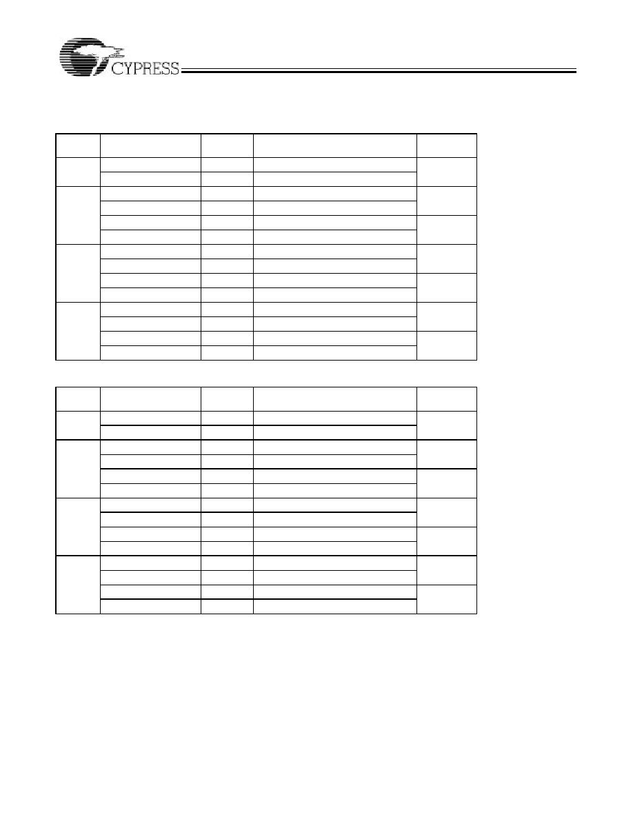
Table 1. Non-Contending Read/Write.
Inputs
Outputs
CE
R/W
OE
SEM
I/O
0
-
7/8
Operation
H
X
X
H
High Z
Power-Down
H
H
L
L
Data Out
Read Data in
Semaphore
X
X
H
X
High Z
I/O Lines Disabled
H
X
L
Data In
Write to Semaphore
L
H
L
H
Data Out
Read
L
L
X
H
Data In
Write
L
X
X
L
Illegal Condition
Table 2. Interrupt Operation Example (assumes BUSY
L
=BUSY
R
=HIGH).
Left Port
Right Port
Function
R/W
CE
OE
A
0
-
12
INT
R/W
CE
OE
A
0
-
12
INT
Set Left INT
X
X
X
X
L
L
L
X
1FFE
X
Reset Left INT
X
L
L
1FFE
H
X
L
L
X
X
Set Right INT
L
L
X
1FFF
X
X
X
X
X
L
Reset Right INT
X
X
X
X
X
X
L
L
1FFF
H
Table 3. Semaphore Operation Example.
Function
I/O
0-7/8
Left
I/O
0-7/8
Right
Status
No action
1
1
Semaphore free
Left port writes semaphore
0
1
Left port obtains semaphore
Right port writes 0 to semaphore
0
1
Right side is denied access
Left port writes 1 to semaphore
1
0
Right port is granted access to semaphore
Left port writes 0 to semaphore
1
0
No change. Left port is denied access
Right port writes 1 to semaphore
0
1
Left port obtains semaphore
Left port writes 1 to semaphore
1
1
No port accessing semaphore address
Right port writes 0 to semaphore
1
0
Right port obtains semaphore
Right port writes 1 to semaphore
1
1
No port accessing semaphore
Left port writes 0 to semaphore
0
1
Left port obtains semaphore
Left port writes 1 to semaphore
1
1
No port accessing semaphore
CY7C145
CY7C144
16
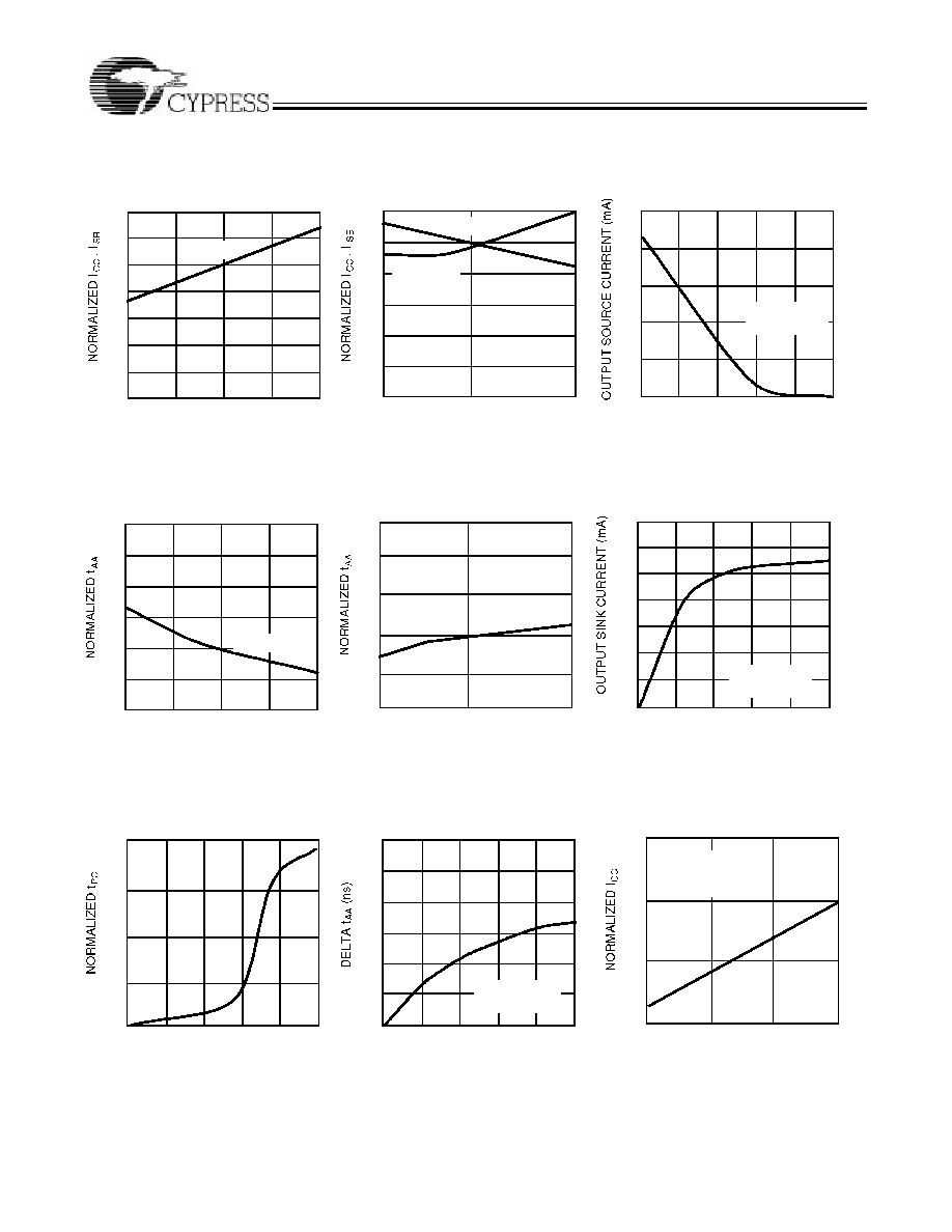
Typical DC and AC Characteristics
1.4
1.0
0.4
4.0
4.5
5.0
5.5
6.0
-
55
25
125
1.2
1.0
120
80
0
1.0
2.0
3.0
4.0
SUPPLY VOLTAGE (V)
NORMALIZED SUPPLY CURRENT
vs. SUPPLY VOLTAGE
NORMALIZED SUPPLY CURRENT
vs. AMBIENT TEMPERATURE
AMBIENT TEMPERATURE (°C)
OUTPUT VOLTAGE (V)
OUTPUT SOURCE CURRENT
vs. OUTPUT VOLTAGE
0.0
0.8
0.8
0.6
0.6
V
CC
=5.0V
V
IN
=5.0V
0
I
CC
I
CC
1.6
1.4
1.2
1.0
0.8
-
55
125
NORMALIZED ACCESS TIME
vs. AMBIENT TEMPERATURE
AMBIENT TEMPERATURE (°C)
1.4
1.3
1.2
1.0
0.9
4.0
4.5
5.0
5.5
6.0
SUPPLY VOLTAGE (V)
NORMALIZED ACCESS TIME
vs. SUPPLY VOLTAGE
120
140
100
60
40
20
0.0
1.0
2.0
3.0
4.0
0
80
OUTPUT VOLTAGE (V)
OUTPUT SINK CURRENT
vs. OUTPUT VOLTAGE
V
CC
=5.0V
T
A
=25°C
0.6
0.8
V
CC
=5.0V
T
A
=25°C
1.25
1.0
0.75
10
0.50
NORMALIZED I
CC
vs. CYCLE TIME
CYCLE FREQUENCY (MHz)
25.0
30.0
20.0
10.0
5.0
0
200
400
600
800
0
15.0
SUPPLY VOLTAGE (V)
TYPICAL POWER-ON CURRENT
vs. SUPPLY VOLTAGE
CAPACITANCE (pF)
TYPICAL ACCESS TIME CHANGE
vs. OUTPUT LOADING
1000
28
0.2
0.6
1.2
I
SB3
0.2
0.4
I
SB3
25
1.1
V
CC
=4.5V
T
A
=25°C
V
CC
=5.0V
T
A
=25°C
V
IN
=0.5V
5.0
V
CC
=5.0V
T
A
=25°C
40
160
200
5.0
40
66
1.00
0.25
0
1.0
2.0
3.0
5.0
0.0
4.0
0.50
0.75
CY7C145
CY7C144
17
8K x9 Dual-Port SRAM
Ordering Information
8K x8 Dual-Port SRAM
Speed
(ns)
Ordering Code
Package
Name
Package Type
Operating
Range
15
CY7C144-15AC
A65
64-Lead Thin Quad Flat Pack
Commercial
CY7C144-15JC
J81
68-Lead Plastic Leaded Chip Carrier
25
CY7C144-25AC
A65
64-Lead Thin Quad Flat Pack
Commercial
CY7C144-25JC
J81
68-Lead Plastic Leaded Chip Carrier
CY7C144-25AI
A65
64-Lead Thin Quad Flat Pack
Industrial
CY7C144-25JI
J81
68-Lead Plastic Leaded Chip Carrier
35
CY7C144-35AC
A65
64-Lead Thin Quad Flat Pack
Commercial
CY7C144-35JC
J81
68-Lead Plastic Leaded Chip Carrier
CY7C144-35AI
A65
64-Lead Thin Quad Flat Pack
Industrial
CY7C144-35JI
J81
68-Lead Plastic Leaded Chip Carrier
55
CY7C144-55AC
A65
64-Lead Thin Quad Flat Pack
Commercial
CY7C144-55JC
J81
68-Lead Plastic Leaded Chip Carrier
CY7C144-55AI
A65
64-Lead Thin Quad Flat Pack
Industrial
CY7C144-55JI
J81
68-Lead Plastic Leaded Chip Carrier
Speed
(ns)
Ordering Code
Package
Name
Package Type
Operating
Range
15
CY7C145-15AC
A80
80-Lead Thin Quad Flat Pack
Commercial
CY7C145-15JC
J81
68-Lead Plastic Leaded Chip Carrier
25
CY7C145-25AC
A80
80-Lead Thin Quad Flat Pack
Commercial
CY7C145-25JC
J81
68-Lead Plastic Leaded Chip Carrier
CY7C145-25AI
A80
80-Lead Thin Quad Flat Pack
Industrial
CY7C145-25JI
J81
68-Lead Plastic Leaded Chip Carrier
35
CY7C145-35AC
A80
80-Lead Thin Quad Flat Pack
Commercial
CY7C145-35JC
J81
68-Lead Plastic Leaded Chip Carrier
CY7C145-35AI
A80
80-Lead Thin Quad Flat Pack
Industrial
CY7C145-35JI
J81
68-Lead Plastic Leaded Chip Carrier
55
CY7C145-55AC
A80
80-Lead Thin Quad Flat Pack
Commercial
CY7C145-55JC
J81
68-Lead Plastic Leaded Chip Carrier
CY7C145-55AI
A80
80-Lead Thin Quad Flat Pack
Industrial
CY7C145-55JI
J81
68-Lead Plastic Leaded Chip Carrier
CY7C145
CY7C144
18
Package Diagrams
64-Pin Thin Plastic Quad Flat Pack A65
80-Pin Thin Plastic Quad Flat Pack A80
CY7C145
CY7C144
© Cypress Semiconductor Corporation, 1996. The information contained herein is subject to change without notice. Cypress Semiconductor Corporation assumes no responsibility for the use
of any circuitry other than circuitry embodied in a Cypress Semiconductor product. Nor does it convey or imply any license under patent or other rights. Cypress Semiconductor does not authorize
its products for use as critical components in life-support systems where a malfunction or failure may reasonably be expected to result in significant injury to the user. The inclusion of Cypress
Semiconductor products in life-support systems application implies that the manufacturer assumes all risk of such use and in doing so indemnifies Cypress Semiconductor against all charges.
Package Diagrams (continued)
68-Lead Plastic Leaded ChipCarrierJ81