LUPA
1.3 Mpixel @ 450 fps CMOS APS
04-Jul-03 14:22
1/27
LUPA1300
High speed CMOS image sensor
Data sheets

LUPA
1.3 Mpixel @ 450 fps CMOS APS
04-Jul-03 14:22
2/27
Table of contents
1 I
NTRODUCTION
.............................................................................................................3
2 G
ENERAL DESCRIPTION
................................................................................................3
2.1
CMOS
IMAGE SENSOR ARCHITECTURE
......................................................................................... 3
2.2
P
IXEL ARCHITECTURE
.................................................................................................................... 4
2.3
C
OLUMN READOUT AMPLIFIERS
..................................................................................................... 4
2.4
O
UTPUT AMPLIFIERS
...................................................................................................................... 5
2.5
X-Y
ADDRESSING AND WINDOWING
.............................................................................................. 6
2.6
T
EMPERATURE REFERENCE
........................................................................................................... 6
3 S
PECIFICATIONS
...........................................................................................................8
3.1
G
ENERAL SPECIFICATIONS
............................................................................................................. 8
3.2
E
LECTRICAL CHARACTERISTICS
.................................................................................................... 8
3.3
O
PTICAL CHARACTERISTICS
.......................................................................................................... 9
4 P
IN CONFIGURATION
...................................................................................................10
4.1
P
OWER SUPPLIES AND GROUNDS
.................................................................................................. 14
4.2
B
IASING AND ANALOG SIGNALS
................................................................................................... 14
4.3
P
IXEL ARRAY SIGNALS
................................................................................................................ 15
4.4
D
IGITAL SIGNALS
........................................................................................................................ 18
4.5
T
EST SIGNALS
.............................................................................................................................. 19
5 T
IMING
.......................................................................................................................20
5.1
T
IMING OF THE PIXEL ARRAY
....................................................................................................... 20
5.2
R
EADOUT OF THE PIXEL ARRAY
................................................................................................... 21
5.3
F
RAME RATE CALCULATION
........................................................................................................ 23
5.4
T
IMING OF THE
S
ERIAL
P
ARALLEL
I
NTERFACE
(SPI)................................................................... 23
6 A
PPLICATION NOTES
& FAQ......................................................................................26
APPENDIX A: LUPA-1300 E
VALUATION KIT
................................................................27
LUPA
1.3 Mpixel @ 450 fps CMOS APS
04-Jul-03 14:22
3/27
1 Introduction
This document describes the interfacing and the driving of the image sensor LUPA, which is a 1280 by
1024 CMOS pixel array working at 450 frames/sec. It allows the user to develop a camera system based
on the described timing and interfacing.
2 General
description
The LUPA sensor is a 1280 by 1024 active pixel sensor with synchronous shutter, processed in the Tower
in TS50 process. The pixel size is 14 * 14 um2 and the sensor is designed to achieve a fame rate of 450
frames/sec at full resolution. This high frame rate can be achieved by 16 parallel output amplifiers each
working at 40MHz pixel rate. In the following sections the different modules of the image sensor are
discussed more into detail.
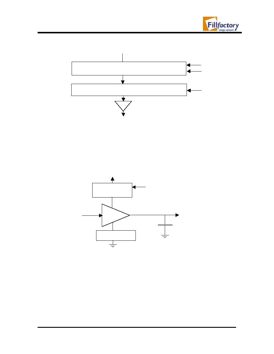
2.1 CMOS image sensor architecture
The image sensor consists of the pixel array, the column readout electronics, X-and Y addressing, on chip
drivers, the output amplifiers and some logic.
Figure 1 : architecture of the LUPA sensor
Figure 1 shows a schematic representation of the image sensor on which the different modules are
displayed.
The image core is a pixel array of 1280 * 1024 pixels each of 14 *14 �m2 in size. The readout is from
bottom left to top right. To obtain a frame rate of 450 frames/sec for this resolution, we have chosen 16
U
p
loadable Y-start
p
osi
t
i
on
LOGIC
Column readout
Y-address
X-address
Uploadable X- startposition
1280 * 1024
Pixel array
1 2 3
14 15 16
Output amplifiers
Drivers for the pixel array signals
LUPA
1.3 Mpixel @ 450 fps CMOS APS
04-Jul-03 14:22
4/27
output amplifiers each capable of driving an output capacitance of 20 pF at 40MHz.
The column readout amplifiers bring the pixel data to the output amplifiers. The logic and the x- and y
addressing controls the image sensor so that progressive scan and windowing is possible. Extra pixel array
drivers are foreseen at the top of the image sensor to control the global pixel array signals.
2.2 Pixel
architecture
The active pixels allow synchronous shutter "i.e. all pixels are illuminated during the same integration
time, starting from the same moment in time. After a certain integration time, the pixels are readout
sequentially. Readout and integration are in parallel, which means that when the image sensor is readout,
the integration time for the next frame is ongoing. This feature requires a memory element inside the pixel,
which affects the maximum fill factor. A schematic representation of the pixel is given in figure 2.
precharge
reset
sample
Row
select
C
o
l
u
m
n
out
Vpix
Mem
Figure 2 : schematic representation of the synchronous pixel as used in the LUPA design
The signals mentioned in figure 2 are the internal signals, generated by the internal drivers, required to
have the synchronous shutter feature.
The photodiode is designed to obtain a sensitivity as high as possible for a dynamic range of at least 60dB.
Consequently the photodiode capacitance is 10fF @ the output, resulting in a S/N of more than 60dB as the
rms noise level is within the expectation of 45 noise electrons.
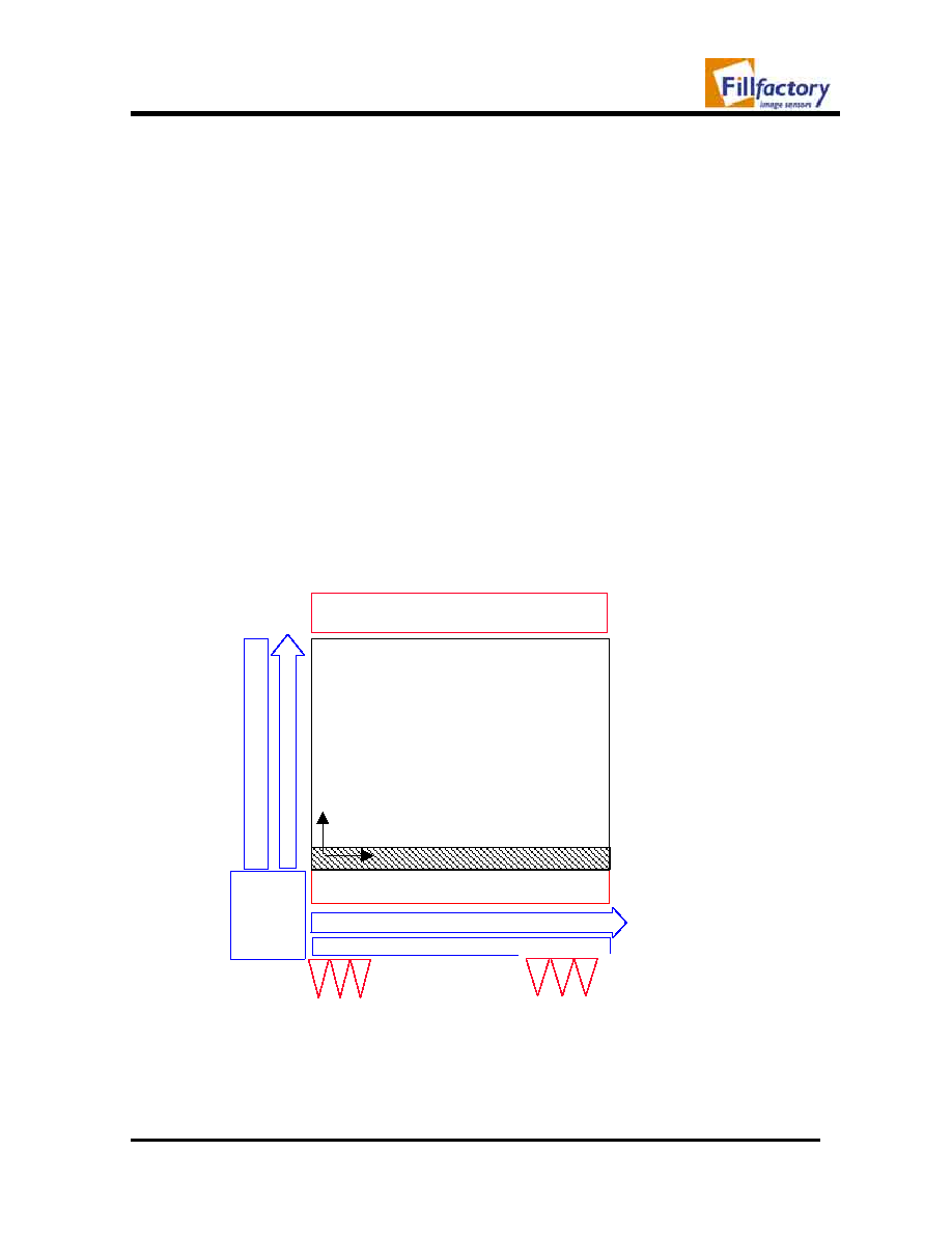
2.3 Column readout amplifiers
The column readout amplifiers are the interface between the pixels and the output amplifiers. The pixels in
the array are selected line by line and the pixels of the selected line are connected to the column readout
amplifiers, which bring the pixel data in the correct format to the output amplifiers.
To obtain a high frame rate, the complexity and the number of stages in the column readout amplifiers
must be minimized, so that the power dissipation remains as low as possible, but also to minimize the row
blanking time. Figure 3 is a schematic representation of the column readout structure. It consists of 2
parts. The first part is a module that reduces the row blanking time. The second part shifts the signal to the
correct level for the output amplifiers and allows multiplexing in the x-direction.
From the moment that a new row is selected, the pixel data of that row is placed onto the columns of the
pixel array. These columns are long lines and have a large parasitic capacitance. As the pixel is small, it is
not possible to match the transistor inside the pixel, which drives this column. Consequently, the first
module in the column readout amplifiers must solve the mismatch between the pixel driver and the large
column capacitance. In this image sensor we have implemented 2 methods to obtain a short line blanking
time. The first baseline method is a straight forward track and hold method. The second method is based
on a new technique, which brings the columns to a reference level before the row is selected. This
technique results in a shorter row blanking time (< 200nsec), reduced power dissipation and an increase
voltage swing.
LUPA
1.3 Mpixel @ 450 fps CMOS APS
04-Jul-03 14:22
5/27
Figure 3 : Schematic representation of the column readout structure.
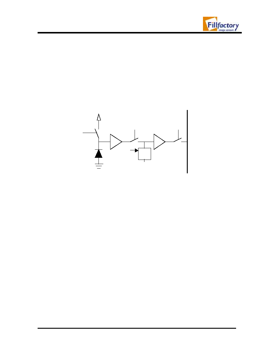
2.4 Output
amplifiers
16 output amplifiers each capable of working at 40MHz pixel rate are placed equidistant on the bottom of
the image sensor. These output amplifiers are required to obtain a frame rate of 450 frames/sec. A single
output stage, not only to reduce power, but also to achieve the required pixel rate is designed. Figure 4 is a
schematic representation of this module and figure 5 shows output curves one can expect from these output
amplifiers.
Figure 4 : schematic representation of a single output stage.
Each output stage is designed to drive a load of 20pF at a pixel rate of 40MHz. The load in the output
stage determines this pixel rate. In case the load capacitance is less than 20pF, the load in the output stage
can increase, resulting in less power dissipation of the output stages and consequently of the whole sensor.
Additionally, decreasing the load of the output stage allows having more current available for the output
stage to charge or discharge the load capacitance to obtain a higher pixel rate.
To avoid variations on the supply voltage to be seen on the output signal, a special module to stabilize the
power supply is required. This module that requires an additional supply voltage (Vstable) allows variation
on the supply voltage Voo without being seen on the output signal.
One can also choose to have a passive load of chip instead of the active output stage load. This
deteriorates the linearity of the output stages, but decreases the power dissipation, as the dissipation in the
load is external.
Output stage
column
Module1 : Track & hold or reference set method
Module 2 : signal conditioning and multiplexing
X-mux
Sh kol
Norow sel
Stabilize power
supply
Vstable
Voo
In
Out
Output stage load
Cload 20 pF