 | –≠–ª–µ–∫—Ç—Ä–æ–Ω–Ω—ã–π –∫–æ–º–ø–æ–Ω–µ–Ω—Ç: DS1236A | –°–∫–∞—á–∞—Ç—å:  PDF PDF  ZIP ZIP |

1 of 20
111899
FEATURES
Holds microprocessor in check during power
transients
Halts and restarts an out-of-control
microprocessor
Monitors pushbutton for external override
Warns microprocessor of an impending power
failure
Converts CMOS SRAM into nonvolatile
memory
Unconditionally write protects memory when
power supply is out of tolerance
Consumes less than 100 nA of battery current
at 25∞C
Controls external power switch for high
current applications
Accurate 10% power supply monitoring
Optional 5% power supply monitoring
designated DS1236A-5
Provides orderly shutdown in nonvolatile
microprocessor applications
Supplies necessary control for low-power
"stop mode" in battery operated hand-held
applications
Standard 16-pin DIP or space-saving 16-pin
SOIC
Optional industrial temperature range -40∞C
to +85∞C
PIN ASSIGNMENT
PIN DESCRIPTION
V
BAT
- +3-Volt Battery Input
V
CCO
- Switched SRAM Supply Output
V
CC
- +5-Volt Power Supply Input
GND -
Ground
PF
- Power-Fail (Active High)
PF
- Power-Fail (Active Low)
WC/
SC
- Wake-Up Control (Sleep)
RC
- Reset Control
IN
- Early Warning Input
NMI
-
Non-Maskable
Interrupt
ST
- Strobe Input
CEO
- Chip Enable Output
CEI
- Chip Enable Input
PBRST
- Pushbutton Reset Input
RST
- Reset Output (Active Low)
RST
- Reset Output (Active High)
DESCRIPTION
The DS1236A MicroManager Chip provides all the necessary functions for power supply monitoring,
reset control, and memory backup in microprocessor-based systems. A precise internal voltage reference
and comparator circuit monitor power supply status. When an out-of-tolerance condition occurs, the
microprocessor reset and power-fail outputs are forced active, and static RAM control unconditionally
write protects external memory. The DS1236A also provides early warning detection of a user-defined
threshold by driving a non-maskable interrupt. External reset control is provided by a pushbutton reset
DS1236A
MicroManager Chip
www.dalsemi.com
16-Pin SOIC (300-mil)
See Mech. Drawings Section
VBAT
VCCO
VCC
RST
RST
PBRST
1
2
3
16
15
14
GND
CEI
4
13
PF
PF
WC/SC
CEO
ST
NMI
5
6
7
12
11
10
RC
IN
8
9
16-Pin DIP (300-mil)
See Mech. Drawings Section
VBAT
VCCO
VCC
RST
RST
PBRST
1
2
3
16
15
14
GND
CEI
4
13
PF
PF
WC/SC
CEO
ST
NMI
5
6
7
12
11
10
RC
IN
8
9

DS1236A
2 of 20
input which is debounced and activates reset outputs. An internal watchdog timer can also force the reset
outputs to the active state if the strobe input is not driven low prior to watchdog timeout. Reset control
and wake-up/sleep control inputs also provide the necessary signals for orderly shutdown and start-up in
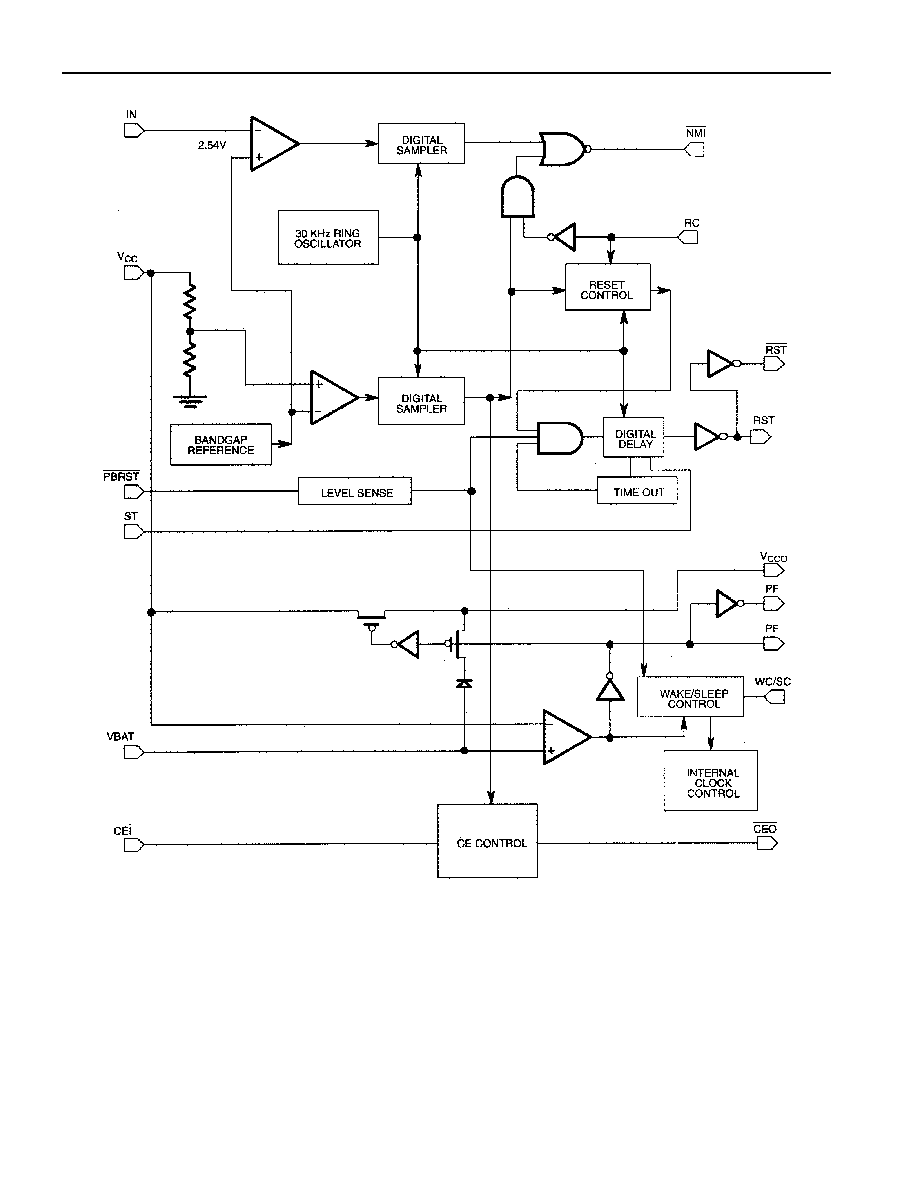
battery backup and battery operated applications. A block diagram of the DS1236A is shown in NO TAG.
PIN DESCRIPTION
PIN NAME
DESCRIPTION
V
BAT
+3V battery input provides nonvolatile operation of control functions.
V
CCO
V
CC
output for nonvolatile SRAM applications.
V
CC
+5V primary power input.
PF
Power-fail indicator, active high, used for external power switching as shown in NO
TAG.
PF
Power-fail indicator, active low.
WC/
SC
Wake-up and Sleep control. Invokes low-power mode.
RC
Reset control input. Determines reset output . Normally low for NMOS processors and
high for battery backed CMOS processors.
IN
Early warning power-fail input. This voltage sense point can be tied (via resistor
divider) to a user-selected voltage.
NMI
Non-maskable interrupt. Used in conjunction with the IN pin to indicate an impending
power failure.
ST
Strobe input. A high-to-low transition will reset the watchdog timer, indicating that
software is still in control.
CEO
Chip enable output. Used with nonvolatile SRAM applications.
CEI
Chip enable input.
PBRST
Pushbutton reset input.
RST
Active low reset output.
RST
Active high reset output.
PROCESSOR MODE
A distinction is often made between CMOS and NMOS processor systems. In a CMOS system, power
consumption may be a concern, and nonvolatile operation is possible by battery backing both the SRAM
and the CMOS processor. All resources would be maintained in the absence of V
CC
. A power-down reset
is not issued since the low-power mode of most CMOS processors (Stop) is terminated with a Reset. A
pulsed interrupt (
NMI
) is issued to allow the CMOS processor to invoke a sleep mode to save power. For
this case, a power-on reset is desirable to wake up and initialize the processor. The CMOS mode is
invoked by connecting RC to V
CCO
.
An NMOS processor consumes more power, and consequently may not be battery backed. In this case, it
is desirable to notify the processor of a power-fail, then keep it in reset during the loss of V
CC
. This avoids
intermittent or aberrant operation. On power-up, the processor will continue to be reset until V
CC
reaches
an operational level to provide an orderly start. The NMOS mode is invoked by connecting RC to ground.

DS1236A
3 of 20
POWER MONITOR
The DS1236A employs a band gap voltage reference and a precision comparator to monitor the 5-volt
supply (V
CC
) in microprocessor-based systems. When an out-of-tolerance condition occurs, the RST and
RST
outputs are driven to the active state. The V
CC
trip point (V
CCTP
) is set for 10% operation so that the
RST and
RST
outputs will become active as V
CC
falls below 4.5 volts (4.37 typical). The V
CCTP
for the
5% operation option (DS1236A-5) is set for 4.75 volts (4.62 typical). The RST and
RST
signals are
excellent for microprocessor reset control, as processing is stopped at the last possible moment of in-
tolerance V
CC
. On power-up, the RST and
RST
signals are held active for a minimum of 25 ms (100 ms
typical) after V
CCTP
is reached to allow the power supply and microprocessor to stabilize. Note: The
operation described above is obtained with the reset control pin (RC) connected to GND (NMOS mode).
Please review the reset control section for more information.
WATCHDOG TIMER
The DS1236A provides a watchdog timer function which forces the RST and
RST
signals to the active
state when the strobe input (
ST
) is not stimulated for a predetermined time period. This time period is 400
ms typically with a maximum timeout of 600 ms. The watchdog timeout period begins as soon as RST
and
RST
are inactive. If a high-to-low transition occurs at the
ST
input prior to timeout, the watchdog
timer is reset and begins to time out again. The
ST
input timing is shown in NO TAG. To guarantee the
watchdog timer does not time out, a high-to-low transition on
ST
must occur at or less than 100 ms
(minimum timeout) from a reset. If the watchdog timer is allowed to time out, the RST and
RST
outputs
are driven to the active state for 25 ms minimum. The
ST
input can be derived from microprocessor
address, data, and/or control signals. Under normal operating conditions, these signals would routinely
reset the watchdog timer prior to timeout. If the watchdog timer is not required, two methods have been
provided to disable it.
Permanently grounding the IN pin in the CMOS mode (RC=1) will disable the watchdog. In normal
operation with RC=1, the watchdog is disabled as soon as the IN pin is below V
TP
. With IN grounded, an
NMI
output will occur only at power-up, or when the
ST
pin is strobed. As shown in the NO TAG, a
falling edge on
ST
will generate an
NMI
when IN is below V
TP
. This allows the processor to verify that
power is between V
TP
and V
CCTP
, as an
NMI
will be returned immediately after the
ST
strobe. The
watchdog timer is not affected by the IN pin when in NMOS mode (RC=0).
If the
NMI
signal is required to monitor supply voltages, the watchdog may also be disabled by leaving
the
ST
input open. Independent of the state of the RC pin, the watchdog is also disabled as soon as V
CC
falls to V
CCTP
.
PUSHBUTTON RESET
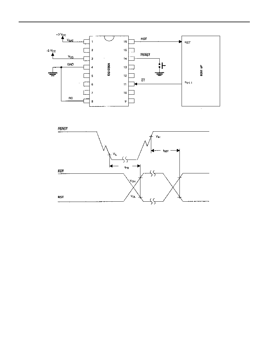
An input pin is provided on the DS1236A for direct connection to a pushbutton. The pushbutton reset
input requires an active low signal. Internally, this input is pulled high by a 10k resistor whenever V
CC
is
greater than V
BAT
. The
PBRST
pin is also debounced and timed such that the RST and
RST
outputs are
driven to the active state for 25 ms minimum. This 25 ms delay begins as the pushbutton is released from
a low level. A typical example of the power monitor, watchdog timer, and pushbutton reset connections
are shown in NO TAG. The
PBRST
input is disabled whenever the IN pin voltage level is less than V
TP
and the reset control (RC) is tied high (CMOS mode). The
PBRST
input is also disabled whenever V
CC
is
below V
BAT
. Timing of the
PBRST
-generated RST is illustrated in Figure 1.

DS1236A
4 of 20
NON-MASKABLE INTERRUPT
The DS1236A generates a non-maskable interrupt
NMI
for early warning of power failure to a
microprocessor. A precision comparator monitors the voltage level at the IN pin relative to a reference
generated by the internal band gap. The IN pin is a high-impedance input allowing for a user-defined
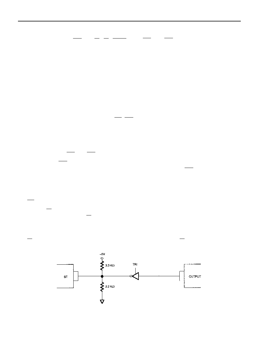
sense point. An external resistor voltage divider network (NO TAG) is used to interface with high voltage
signals. This sense point may be derived from the regulated 5-volt supply or from a higher DC voltage
level closer to the main system power input. Since the IN trip point V
TP
is 2.54 volts, the proper values
for R1 and R2 can be determined by the equation as shown in NO TAG. Proper operation of the
DS1236A requires that the voltage at the IN pin be limited to V
IN
. Therefore, the maximum allowable
voltage at the supply being monitored (V
MAX
) can also be derived as shown in NO TAG. A simple
approach to solving this equation is to select a value for R2 high enough to keep power consumption low,
and solve for R1. The flexibility of the IN input pin allows for detection of power loss at the earliest point
in a power supply system, maximizing the amount of time for microprocessor shutdown between
NMI
and RST or
RST
.
When the supply being monitored decays to the voltage sense point, the DS1236A pulses the
NMI
output
to the active state for a minimum of 200
µ
s. The
NMI
power-fail detection circuitry also has built-in time
domain hysteresis. That is, the monitored supply is sampled periodically at a rate determined by an
internal ring oscillator running at approximately 30 kHz (33
µ
s/cycle). Three consecutive samplings of
out-of-tolerance supply (below V
SENSE
) must occur at the IN pin to activate
NMI
. Therefore, the supply
must be below the voltage sense point for approximately 100
µ
s or the comparator will reset. In this way,
power supply noise is removed from the monitoring function, preventing false trips. During a power-up,
any detected IN pin levels be low V
TP
by the comparator are disabled from reaching the
NMI
pin until
V
CC
rises to V
CCTP
. As a result, any potential
NMI
pulse will not be initiated until V
CC
reaches V
CCTP
.
Removal of an active low level on the
NMI
pin is controlled by either an internal timeout (when IN pin is
less than V
TP
) or by the subsequent rise of the IN pin above V
TP
. The initiation and removal of the
NMI
signal during power-up results in an
NMI
pulse of from 0
µ
s minimum to 500
µ
s maximum, depending
on the relative voltage relationship between V
CC
and the IN pin voltage. As an example, when the IN pin
is tied to ground during power-up, the internal timeout will result in a pulse of 200
µ
s minimum to 500
µ
s
maximum. In contrast, if the IN pin is tied to V
CCO
during power-up,
NMI
will not produce a pulse on
power-up. Note that a fast-slewing power supply may cause the
NMI
to be virtually nonexistent on
power-up. This is of no consequence, however, since an RST will be active.
DS1236A
5 of 20
DS1236A FUNCTIONAL BLOCK DIAGRAM Figure 1

DS1236A
6 of 20
If the IN pin is connected to V
CCO
, the
NMI
output will pulse low as V
CC
decays to V
CCTP
in the NMOS
mode (RC=0). In the CMOS mode (RC=V
CCO
) the power-down of V
CC
out of tolerance at V
CCTP
will not
produce a pulse on the
NMI
pin. Given that any
NMI
pulse has been completed by the time V
CC
decays
to V
CCTP
, the
NMI
pin will remain high. The
NMI
voltage will follow V
CC
down until V
CC
decays to
V
BAT
. Once V
CC
decays to V
BAT
, the
NMI
pin will either remain at V
OHL
or enter tri-state mode as
determined by the RC pin (see "Reset Control" section).
MEMORY BACKUP
The DS1236A provides all of the necessary functions required to battery back a static RAM. First, a
switch is provided to direct SRAM power from the incoming 5-volt supply (V
CC
) or from an external
battery (V
BAT
), whichever is greater. This switched supply (V
CCO
) can also be used to battery back a
CMOS microprocessor. For more information about nonvolatile processor applications, review the "Reset
Control" and "Wake Control" sections. Second, the same power-fail detection described in the power
monitor section is used to hold the chip enable output (
CEO
) to within 0.3 volts of V
CC
or to within 0.7
volts of V
BAT
. This write protection mechanism occurs as V
CC
falls below V
CCTP
as specified. If
CEI
is
low at the time power-fail detection occurs,
CEO
is held in its present state until
CEI
is returned high or
the period t
CE
expires. This delay of write protection until the current memory cycle is completed prevents
the corruption of data. If
CEO
is in an inactive state at the time of V
CC
-fail detection,
CEO
will be
unconditionally disabled within t
CF
. During nominal supply conditions
CEO
will follow
CEI
with a
maximum propagation delay of 20 ns. NO TAG shows a typical nonvolatile SRAM application. The
DS1236A unlike the DS1236 can be operated without a battery. In this method of operation the V
BAT
, pin
1, must be grounded. In general, it would also be expected to have the RC, pin 8, grounded (NMOS
mode) since no battery backup is available.
FRESHNESS SEAL
In order to conserve battery capacity during initial construction of an end system, the DS1236A provides
a freshness seal that electrically disconnects the battery. This means that upon battery attach, the V
CCO
output will remain inactive until V
CC
is applied. This prevents V
CCO
from powering other devices when
the battery is first attached, and V
CC
is not present. Once V
CC
is applied, the freshness seal is broken and
cannot be invoked again without subsequent removal and reattachment of the battery.
POWER SWITCHING
When larger operating currents are required in a battery backed system, the 5-volt supply and battery
supply switches internal to the DS1236A may not be large enough to support the required load through
V
CCO
with a reasonable voltage drop. For these applications, the PF and
PF
outputs are provided to gate
external power switching devices. As shown in Figure 8, power to the load is switched from V
CC
to
battery on power-down, and from battery to V
CC
on power-up. The DS1336 is designed to use the
PF
output to switch between V
BAT
and V
CC
It provides better leakage and switchover performance than
currently available discrete components. The transition threshold for PF and
PF
is set to the external
battery voltage V
BAT
, allowing a smooth transition between sources. The load applied to the PF pin from
the external switch will be supplied by the battery. Therefore, if a discrete switch is used, this load should
be taken into consideration when sizing the battery.
RESET CONTROL
As mentioned above, the DS1236A supports two modes of operation. The CMOS mode is used when the
system incorporates a CMOS microprocessor which is battery backed. The NMOS mode is used when a
non-battery backed processor is incorporated. The mode is selected by the RC (Reset Control) pin. The
level of this pin distinguishes timing and level control on RST,
RST
, and
NMI
outputs for volatile
processor operation versus nonvolatile battery backup or battery-operated processor applications.

DS1236A
7 of 20
ST/INPUT TIMING Figure 2
NMI/FROM ST/INPUT Figure 3
DS1236A
8 of 20
POWER MONITOR, WATCHDOG Figure 4
PUSHBUTTON RESET TIMING Figure 5
DS1236A
9 of 20
NON-MASKABLE INTERRUPT Figure 6
EXAMPLE 1: 5-VOLT SUPPLY, R2 = 10k OHM, V
SENSE
= 4.80 VOLTS
4.80 =
10k
10k
R1
+
X 2.54
R1 = 8.9k OHM
EXAMPLE 2: 12-VOLT SUPPLY, R2 = 10k OHM, V
SENSE
= 9.00 VOLTS
9.00 =
10k
10k
R1
+
X 2.54
R1 = 25.4k OHM
V
MAX
=
2.54
9.00 X 5.00 = 17.7 VOLTS
NONVOLATILE SRAM Figure 7

DS1236A
10 of 20
When the RC pin is tied to ground, the DS1236A is designed to interface with NMOS processors which
do not have the microamp currents required during a battery backed mode. Grounding the RC pin does,
however, continue to support nonvolatile backup of system SRAM memory. Nonvolatile systems
incorporating NMOS processors generally require that only the SRAM memory and/or timekeeping
functions be battery backed. When the processor is not battery backed (RC = 0), all signals connected
from the processor to the DS1236A are disconnected from the backup battery supply, or grounded when
system V
CC
decays below V
BAT
. In the NMOS processor system, the principal emphasis is placed on
giving early warnings with
NMI
, then providing a continuously active RST and
RST
signal during
power-down while isolating the backup battery from the processor during a loss of V
CC
.
During power-down,
NMI
will pulse low for a minimum of 200
µ
s, and then return high. If RC is tied
low (NMOS mode), the voltage on
NMI
will follow V
CC
until V
CC
supply decays to V
BAT
, at which point
NMI
will enter tri-state (see timing diagram). Also, upon V
CC
out of tolerance at V
CCTP
, the RST and
RST
outputs are driven active and RST will follow V
CC
as the supply decays. On power-up, RST follows
V
CC
up,
RST
is held low, and both remain active for t
RST
after valid V
CC
. During a power-up from a V
CC
voltage below V
BAT
, any detected IN pin levels below V
TP
are disabled from reaching the
NMI
pin until
V
CC
rises to V
CCTP
. As a result, any potential
NMI
pulse will not be initiated until V
CC
reaches V
CCTP
.
Removal of an active low level on the
NMI
pin is controlled by either an internal timeout (when the IN
pin is less than V
TP
), or by the subsequent rise of the IN pin above V
TP
. The initiation and removal of the
NMI
signal results in an
NMI
pulse of 0
µ
s minimum to 500
µ
s maximum during power-up, depending
on the relative voltage relationship between V
CC
and the IN pin. As an example, when the IN pin is tied to
ground, the internal timeout will result in a pulse of 200
µ
s minimum to 500
µ
s maximum. In contrast, if
the IN pin is tied to V
CCO
,
NMI
will not produce a pulse on power-up.
Connecting the RC pin to a high (V
CCO
) invokes CMOS mode and provides nonvolatile support to both
the system SRAM as well as a low power CMOS processor. When using CMOS microprocessors, it is
possible to place the microprocessor into a very low-power mode termed the "stop" or "halt" mode. In
this state the CMOS processor requires only microamp currents and is fully capable of being battery
backed. This mode generally allows the CMOS microprocessor to maintain the contents of internal RAM
as well as state control of I/O ports during battery backup. The processor can subsequently be restarted by
any of several different signals. To maintain this low-power state, the DS1236A issues no
NMI
and/or
reset signals to the processor until it is time to bring the processor back into full operation. To support the
low-power processor battery backed mode (RC = 1), the DS1236A provides a pulsed
NMI
for early
power failure warning. Waiting to initiate a Stop mode until after the
NMI
pin has returned high will
guarantee the processor that no other active
NMI
or RST/
RST
will be issued by the DS1236A until one
of two conditions occurs: 1) Voltage on the pin rises above V
TP
, which activates the watchdog, or 2) V
CC
cycles below then above V
BAT
, which also results in an active RST and
RST
. If V
CC
does not fall below
V
CCTP
, the processor will be restarted by the reset derived from the watchdog timer as the IN pin rises
above V
TP
.
With the RC pin tied to V
CCO
, RST and
RST
are not forced active as V
CC
collapses to V
CCTP
. The
RST
is
held at a high level via the external battery as V
CC
falls below battery potential. This mode of operation is
intended for applications in which the processor is made nonvolatile with an external source, and allows
the processor to power down into a Stop mode as signaled from
NMI
at an earlier voltage level. The
NMI
output pin will pulse low for t
NMI
following a low voltage detect at the IN pin of V
TP
. Following t
NMI
,
however,
NMI
will also be held at a high level (V
BAT
) by the battery as V
CC
decays below V
BAT
. On
power-up, RST and
RST
are held inactive until V
CC
reaches V
BAT
, then RST and
RST
are driven active
for t
RST
. If the IN pin falls below V
TP
during an active reset, the reset outputs will be forced inactive by

DS1236A
11 of 20
the
NMI
output. In addition, as long as the IN pin is less than V
TP
, stimulation of the ST pin will result in
additional
NMI
pulses. In this way, the
ST
pin can be used to allow the CMOS processor to determine if
the supply voltage, as monitored by the IN pin, is above or below a selected operating value. This is
illustrated in NO TAG. As discussed above, the RC pin determines the timing relationships and levels of
several signals. The following section describes the power-up and power-down timing diagrams in more
detail.
TIMING DIAGRAMS
This section provides a description of the timing diagrams shown in Figure 9, Figure 10, Figure 11, and
Figure 12. These diagrams show the relative timing and levels in both the NMOS and the CMOS mode
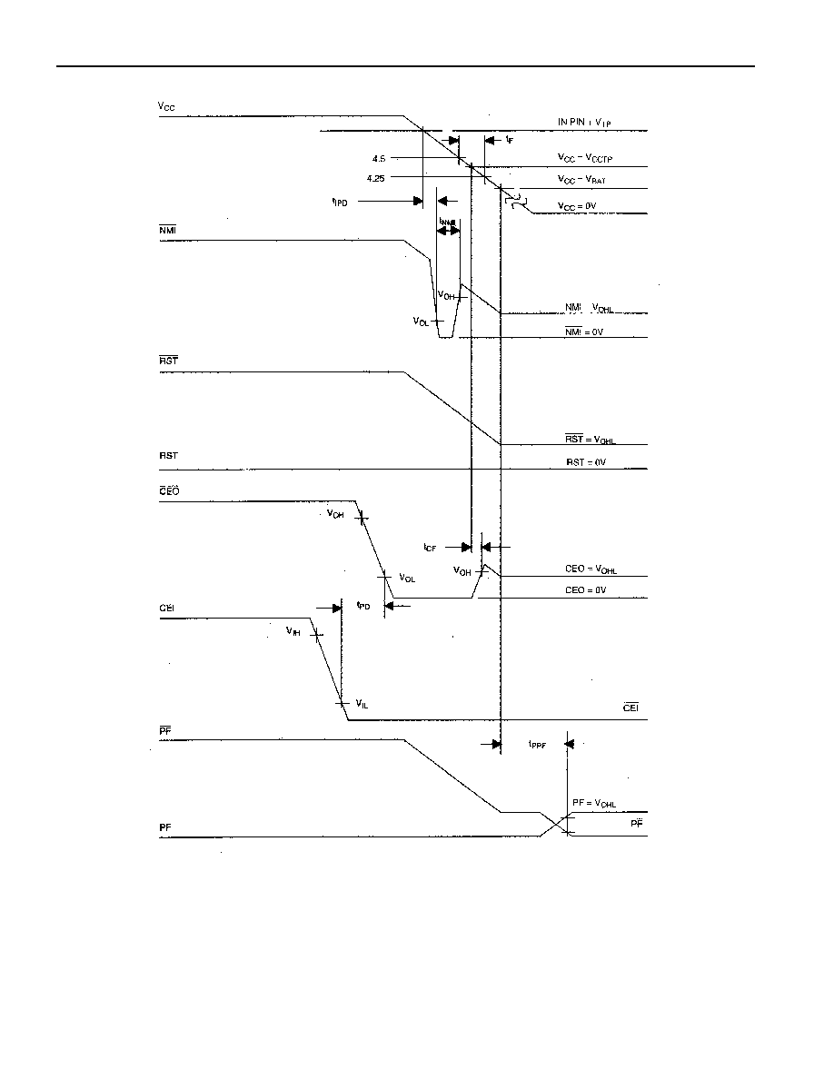
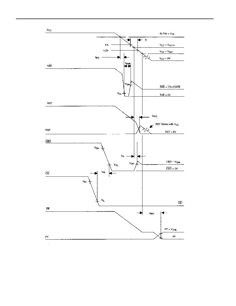
for power-up and down. Figure 9 illustrates the relationship for power-down in CMOS mode. As V
CC
falls, the IN pin voltage drops below V
TP
. As a result, the processor is notified of an impending power
failure via an active
NMI
, which allows it to enter a sleep mode. As the power falls further, V
CC
crosses
V
CCTP
, the power monitor trip point. Since the DS1236A is in CMOS mode, no reset is generated. The
RST
voltage will follow V
CC
down, but will fall no further than V
BAT
. At this time,
CEO
is brought high
to write protect the RAM. When the V
CC
reaches V
BAT
, a power-fail is issued via the PF and
PF
pins.
Figure 10 illustrates operation of the power-down sequence in NMOS mode. Once again, as power falls,
an
NMI
is issued. This gives the processor time to save critical data in nonvolatile SRAM. When V
CC
reaches V
CCTP
, an active RST and
RST
are given. The RST voltage will follow V
CC
as it falls.
CEO
, PF,
and
PF
will operate in a similar manner to CMOS mode. Notice that the
NMI
will tri-state to prevent a
loss of battery power.
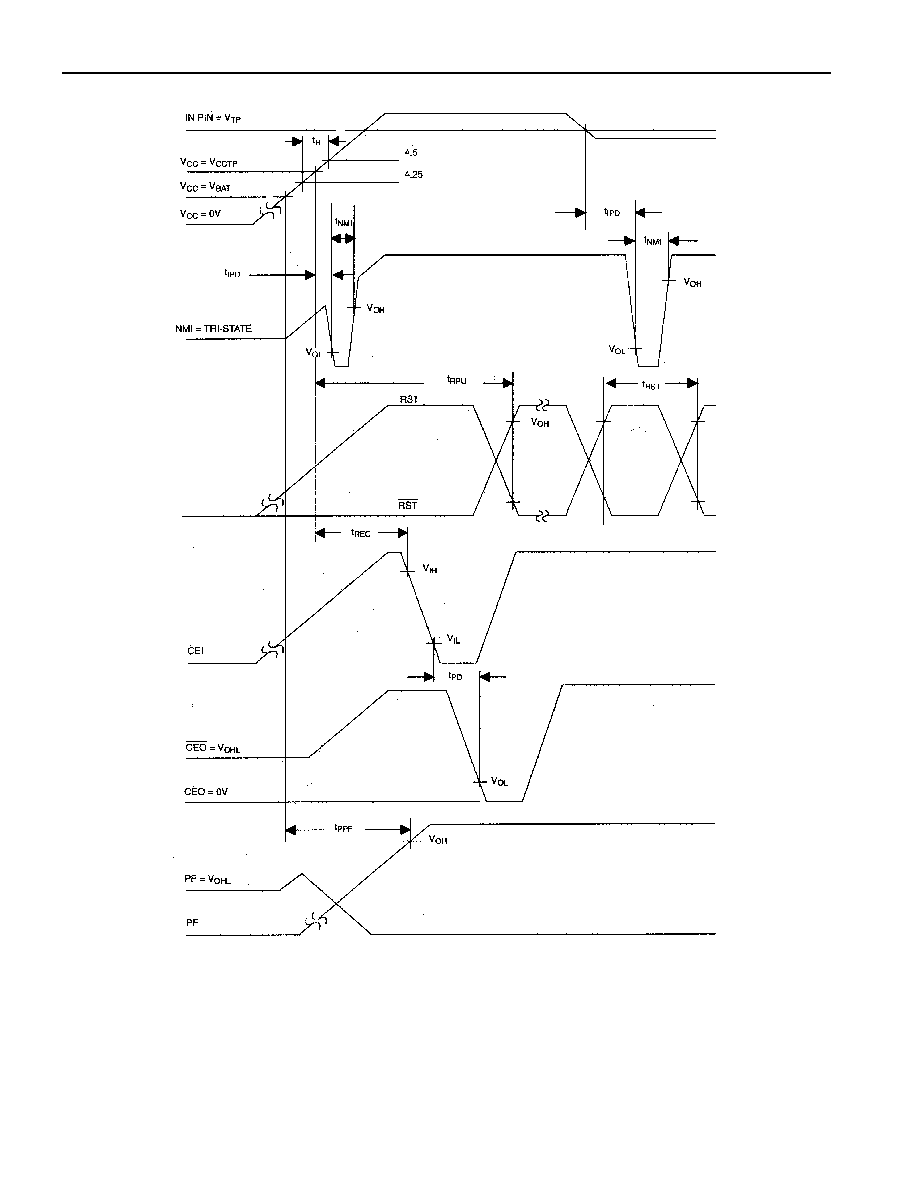
Figure 11 shows the power-up sequence for the NMOS mode. As V
CC
slews above V
BAT
, the PF and
PF
pins are deactivated. An active reset occurs as well as an
NMI
. Although the
NMI
may be short due to
slew rates, reset will be maintained for the standard t
RST
timeout period. At a later time, if the IN pin falls
below V
TP
, a new
NMI
will occur. If the processor does not issue a
ST
, a watchdog reset will also occur.
The second
NMI
and RST are provided to illustrate these possibilities.
Figure 12 illustrates the power-up timing for CMOS mode. The principal difference is that the DS1236A
issues a reset immediately in the NMOS mode. In CMOS mode, a reset is issued when IN rises above
V
TP
. Depending on the processor type, the
NMI
may terminate the Stop mode in the processor.
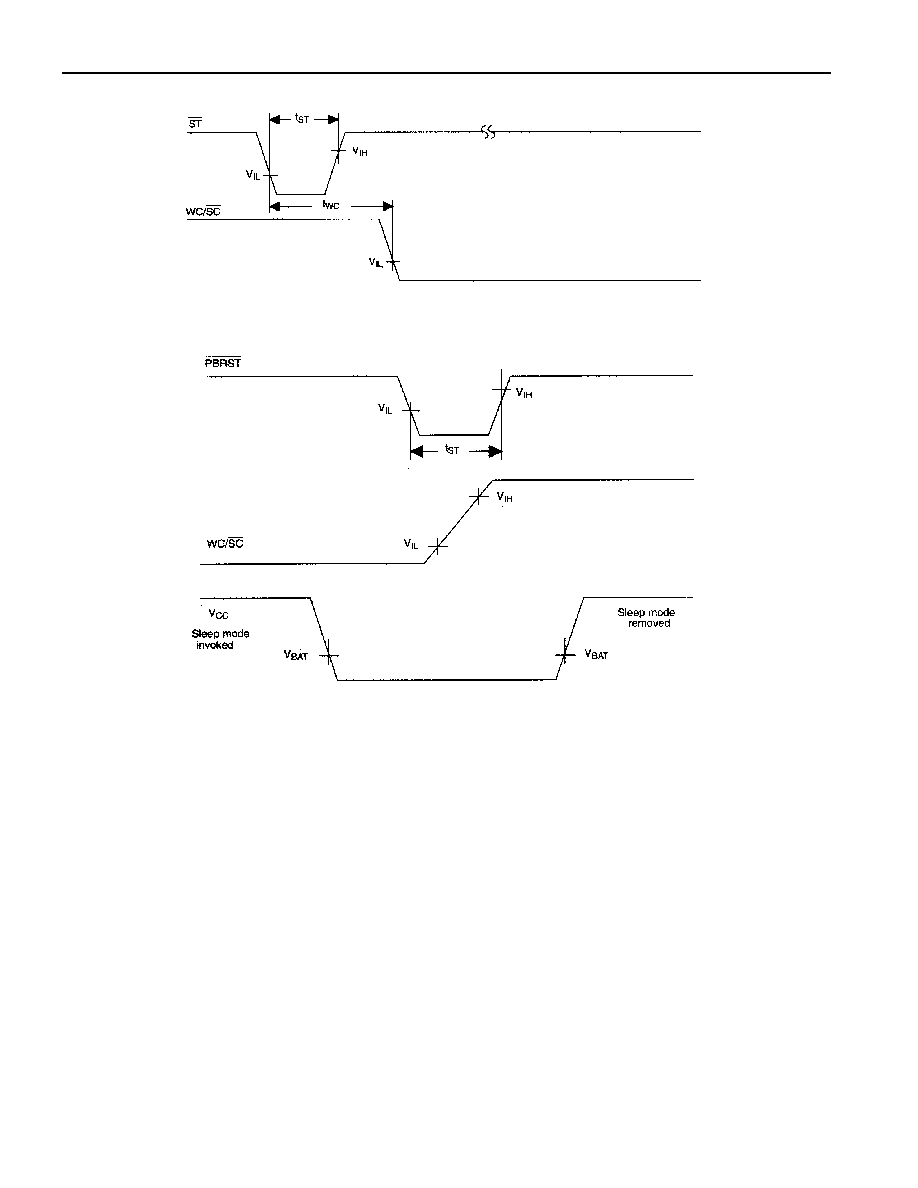
WAKE CONTROL/SLEEP CONTROL
The Wake/Sleep Control input (WC/
SC
) allows the processor to disable all comparators on the DS1236A
before entering the Stop mode. This feature allows the DS1236A, processor, and static RAM to maintain
nonvolatility in the lowest power mode possible. The processor may invoke the sleep mode in battery-
operated applications to conserve battery capacity when an absence of activity is detected. The operation
of this signal is shown in Figure 13. The DS1236A may subsequently be restarted by a high-to-low
transition on the
PBRST
input through human interface via a keyboard, touchpad, etc. The processor will
then be restarted as the watchdog times out and drives RST and
RST
active. The DS1236A can also be
started up by forcing the WC/
SC
pin high from an external source. Also, if the DS1236A is placed in a
sleep mode by the processor and system power is lost, the DS1236A will wake up the next time V
CC
rises
above V
BAT
. These possibilities are illustrated in Figure 14.
When the sleep mode is invoked during normal power-valid conditions, all operation on the DS1236A is
disabled, thus leaving the
NMI
, RST, and
RST
outputs disabled as well as the
ST
and IN inputs.
However, a loss of power during a sleep mode will result in an active RST and
RST
when the RC pin is

DS1236A
12 of 20
grounded (NMOS mode). If the RC pin is tied high, the RST and
RST
pins will remain inactive during
power-down in a sleep mode. Removal of the sleep mode by the
PBRST
input is not affected by the IN
pin threshold at V
TP
when the RC pin is tied high (CMOS mode). Subsequent power-up of the V
CC
supply
with the RC pin tied high will activate the RST and
RST
outputs as the main supply rises above V
BAT
. A
high-to-low transition on the WC/
SC
pin must follow a high-to-low transition on the ST pin by t
WC
to
invoke a Sleep mode for the DS1236A.
POWER SWITCHING Figure 8
DS1236A
13 of 20
CMOS MODE POWER-DOWN (RC = V
CCO
) Figure 9
DS1236A
14 of 20
NMOS MODE POWER-DOWN (RC = GND) Figure 10
DS1236A
15 of 20
NMOS MODE POWER-UP (RC = GND) Figure 11

DS1236A
16 of 20
CMOS MODE POWER-UP (RC = V
CCO
) Figure 12
DS1236A
17 of 20
WAKE/SLEEP CONTROL Figure 13
OPTIONS FOR INVOKING WAKEUP Figure 14

DS1236A
18 of 20
ABSOLUTE MAXIMUM RATINGS*
Voltage on V
CC
Pin Relative to Ground
-0.5V to +7.0V
Voltage on I/O Relative to Ground
-0.5V to V
CC
+ 0.5V
Operating Temperature
0∞C to 70∞C
Operating Temperature (Industrial Version)
-40∞C to +85∞C
Storage Temperature
-55∞C to +125∞C
Soldering Temperature
260∞C for 10 seconds
*
This is a stress rating only and functional operation of the device at these or any other conditions
above those indicated in the operation sections of this specification is not implied. Exposure to
absolute maximum rating conditions for extended periods of time may affect reliability.
RECOMMENDED DC OPERATING CONDITIONS (0
∞
C to 70
∞
C)
PARAMETER
SYMBOL
MIN
TYP
MAX
UNITS NOTES
Supply Voltage
V
CC
4.5
5.0
5.5
V
1
Supply Voltage (5% Option)
V
CC
4.75
5.0
5.5
V
1
Input High Level
V
IH
2.0
V
CC
+0.3
V
1
Input Low Level
V
IL
-0.3
+0.8
V
1
IN Input Pin
V
IN
-0.3
V
CC
+0.3
V
1
Battery Input
V
BAT
0
4.0
V
1
DC ELECTRICAL CHARACTERISTICS (0
∞
C to 70
∞
C; V
CC
= 4.5V to 5.5V)
PARAMETER
SYMBOL
MIN
TYP
MAX
UNITS NOTES
Supply Current
I
CC
4
mA
2
Sleep Supply Current in Sleep
Mode
I
CC
20
µ
A
Battery Current
I
BAT
0.1
µ
A
2
Supply Output Current
(V
CCO
=V
CC
- 0.3V)
I
CC01
100
mA
3
Supply Output Current in Data
Retention (V
CC
< V
BAT
)
I
CC02
1
mA
4
Supply Output Voltage
V
CCO
V
CC
-0.3
V
1
Battery Backup Voltage
V
CCO
V
BAT
-0.7
V
1, 6
Low Level @ RST
V
OL
0.4
V
1
Output Voltage @ -500
µ
A
V
OH
V
CC
-0.5V V
CC
-0.1V
V
1
CEO
and PF Output
V
OHL
V
BAT
-0.7
V
1, 6, 19
PBRST
Pull-up Resistor
R
PBRST
10k
Input Leakage Current
I
LI
-1.0
+1.0
µ
A
18
Output Leakage
I
LO
-1.0
+1.0
µ
A
18
Output Current @ 0.4V
I
OL
4.0
mA
12
Output Current @ 2.4V
I
OH
-1.0
mA
13

DS1236A
19 of 20
PARAMETER
SYMBOL
MIN
TYP
MAX
UNITS NOTES
Power Sup. Trip Point
V
CCTP
4.25
4.37
4.50
V
1
Power Supply Trip (5% Option)
V
CCTP
4.50
4.62
4.75
V
1
IN Input Pin Current
I
CCIN
-1.0
+1.0
µ
A
IN Input Trip Point
V
TP
2.5
2.54
2.6
V
1
AC ELECTRICAL CHARACTERISTICS (0
∞
C to 70
∞
C; V
CC
= 4.5V to 5.5V)
PARAMETER
SYMBOL
MIN
TYP
MAX
UNITS NOTES
V
CC
Fail Detect to RST,
RST
t
RPD
40
100
175
µ
s
V
TP
to
NMI
t
IPD
40
100
175
µ
s
RESET Active Time
t
RST
25
100
150
ms
NMI
Pulse Width
t
NMI
200
300
500
µ
s
14
ST
Pulse Width
t
ST
20
ns
20
PBRST
@ V
IL
t
PB
30
ms
V
CC
Slew Rate 4.75 to 4.25
t
F
300
µ
s
Chip Enable Propagation Delay
t
PD
20
ns
V
CC
Fail to Chip Enable High
t
CF
7
12
44
µ
s
17
V
CC
Valid to RST,
RST
(RC=1)
t
FPU
100
ns
V
CC
Valid to RST &
RST
t
RPU
25
100
150
ms
5
V
CC
Slew to 4.24 to V
BAT
t
FB1
10
µ
s
7
V
CC
Slew 4.25 to 4.75 V
BAT
t
FB2
100
µ
s
8
Chip Enable Output Recovery
Time
t
REC
.1
µ
s
9
V
CC
Slew 4.25 to 4.75
t
R
0
µ
s
Chip Enable Pulse Width
t
CE
5
s
10
Watchdog Time Delay
t
TD
100
400
600
ms
ST
to WC/
SC
t
WC
0.1
50
µ
s
V
BAT
Detect to PF,
PF
t
PPF
2
µ
s
7
ST
to
NMI
t
STN
30
ns
11
NMI
to RST &
RST
t
NRT
30
ns
V
BAT
Detect to RST &
RST
t
ARST
200
µ
s
15
V
CC
Valid to RST,
RST
t
BRST
30
100
150
µ
s
16
CAPACITANCE (t
A
=25
∞
C)
PARAMETER
SYMBOL
MIN
TYP
MAX
UNITS NOTES
Input Capacitance
C
IN
5
pF
Output Capacitance
C
OUT
7
pF
DS1236A
20 of 20
NOTES:
1.
All voltages referenced to ground. A 0.1
µ
F capacitor is recommended between V
CC
and GND.
2.
Measured with V
CCO
,
CEO
, PF,
PF
,
ST
,
PBRST
, RST,
RST
, and
NMI
pin open. I
BAT
specified at
25
∞
C.
3.
I
CCO1
is the maximum average load which the DS1236A can supply at V
CC
-0.3V through the V
CCO
pin
during normal 5-volt operation.
4.
I
CCO2
is the maximum average load which the DS1236A can supply through the V
CCO
pin during data
retention battery supply operation, with a maximum drop of 0.8 volts.
5.
With t
R
= 5
µ
s.
6.
V
CCO
is approximately V
BAT
-0.5V at 1
µ
A load.
7.
Sleep mode is not invoked.
8.
Sleep mode is invoked.
9.
t
REC
is the minimum time required before
CEI
/
CEO
memory access is allowed.
10.
t
CE
maximum must be met to ensure data integrity on power loss.
11.
IN input is less than V
TP
but V
CC
greater than V
CCTP
.
12.
All outputs except RST which is 25
µ
A maximum.
13.
All outputs except
RST
and
NMI
, which is 25
µ
A minimum.
14.
Pulse width of
NMI
requires that the IN pin remain below V
TP
. If the IN pin returns to a level above
V
TP
for a period longer than t
IPD
and before the t
NMI
period has elapsed, the
NMI
pin will immediately
return to a high.
15.
IN pin greater than V
TP
when V
CC
supply rises to V
BAT
. Example: IN tied to GND.
16.
IN pin less than V
TP
when V
CC
supply rises to V
BAT
.
17.
CEI
low.
18.
The WC/
SC
pin contains an internal latch which drives back on to the pin. This latch requires +200
µ
amps to switch states. The
ST
pin will sink
±
50
µ
amps in normal operation and
±
1
µ
amp in the
sleep mode.
19.
If no battery is attached (i.e., V
BAT
=GND) then V
OHL
will track V
CC
.
20.
ST
should be active low before the watchdog is disabled (i.e., before the
ST
input is tristated).