 | –≠–ª–µ–∫—Ç—Ä–æ–Ω–Ω—ã–π –∫–æ–º–ø–æ–Ω–µ–Ω—Ç: DS1238A | –°–∫–∞—á–∞—Ç—å:  PDF PDF  ZIP ZIP |
1 of 13
111899
FEATURES
Holds microprocessor in check during power
transients
Halts and restarts an out-of-control
microprocessor
Warns microprocessor of an impending power
failure
Converts CMOS SRAM into nonvolatile
memory
Unconditionally write protects memory when
power supply is out of tolerance
Delays write protection until completion of
the current memory cycle
Consumes less than 200 nA of battery current
Controls external power switch for high
current applications
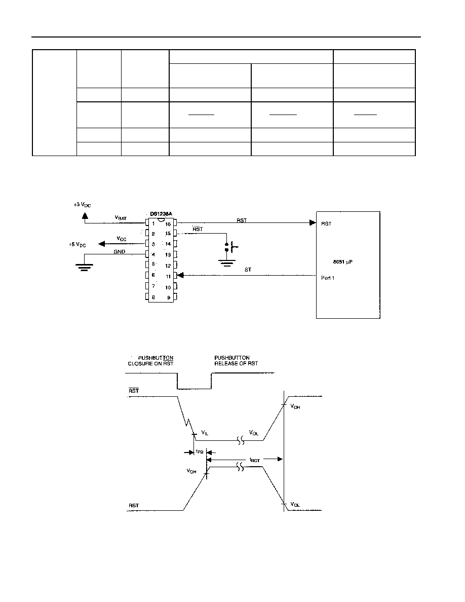
Debounces pushbutton reset
Accurate 10% power supply monitoring
Optional 5% power supply monitoring
designated DS1238A-5
Provides orderly shutdown in microprocessor
applications
Pin-for-pin compatible with MAX691
Standard 16-pin DIP or space-saving 16-pin
SOIC
Optional industrial temperature range -40
∞
C
to +85
∞
C
PIN ASSIGNMENT
PIN DESCRIPTION
V
BAT
- +3-Volt Battery Input
V
CCO
- Switched SRAM Supply Output
V
CC
- +5-Volt Power Supply Input
GND -
Ground
PF -
Power-Fail
RVT
- Reset Voltage Threshold
OSCIN -
Oscillator
In
OSCSEL
- Oscillator Select
IN
- Early Warning Input
NMI
-
Non-Maskable
Interrupt
ST
- Strobe Input
CEO
- Chip Enable Output
CEI
- Chip Enable Input
WDS
- Watchdog Status
RST
- Reset Output (active low)
RST
- Reset Output (active high)
DESCRIPTION
The DS1238A MicroManager provides all the necessary functions for power supply monitoring, reset
control, and memory backup in microprocessor-based systems. A precise internal voltage reference and
comparator circuit monitor power supply status. When an out-of-tolerance condition occurs, the
microprocessor reset and power-fail outputs are forced active, and static RAM control unconditionally
write protects external memory. The DS1238A also provides early warning detection of a user-defined
threshold by driving a non-maskable interrupt. External reset control is provided by a pushbutton reset
DS1238A
MicroManager
www.dalsemi.com
16-Pin SOIC (300-mil)
See Mech. Drawings Section
VBAT
VCCO
VCC
RST
RST
WDS
1
2
3
16
15
14
GND
CEI
4
13
PF
RVT
OSCIN
CEO
ST
NMI
5
6
7
12
11
10
OSCSEL
IN
8
9
16-Pin DIP (300-mil)
See Mech. Drawings Section
VBAT
VCCO
VCC
RST
RST
WDS
1
2
3
16
15
14
GND
CEI
4
13
PF
RVT
OSCIN
CEO
ST
NMI
5
6
7
12
11
10
OSCSEL
IN
8
9

DS1238A
2 of 13
debounce circuit connected to the
RST
pin. An internal watchdog timer can also force the reset outputs to
the active state if the strobe input is not driven low prior to watchdog timeout. Oscillator control pins
OSCSEL and OSCIN provide either external or internal clock timing for both the reset pulse width and
the watchdog timeout period. The Watchdog Status and Reset Voltage Threshold are provided via
WDS
and
RVT
, respectively. A block diagram of the DS1238A is shown in NO TAG.
PIN DESCRIPTION
PIN NAME
DESCRIPTION
V
BAT
+3V battery input provides nonvolatile operation of control functions.
V
CCO
V
CC
output for nonvolatile SRAM applications.
V
CC
+5V primary power input.
PF
Power-fail indicator, active high, used for external power switching as shown in NO
TAG.
RVT
Reset Voltage Threshold. Indicates that V
CC
is below the reset voltage threshold.
OSCIN
Oscillator input or timing capacitor. See NO TAG.
OSCSEL
Oscillator Select. Selects internal or external clock functions. See NO TAG.
IN
Early warning power-fail input. This voltage sense point can be tied (via resistor
divider) to a user-selected voltage.
NMI
Non-maskable interrupt. Used in conjunction with the IN pin to indicate an impending
power failure.
ST
Strobe input. A high-to-low transition will reset the watchdog timer, indicating that
software is still in control.
CEO
Chip enable output. Used with nonvolatile SRAM applications.
CEI
Chip enable input.
WDS
Watchdog Status. Indicates that a watchdog timeout has occurred.
RST
Active low reset output.
RST
Active high reset output.
POWER MONITOR
The DS1238A employs a bandgap voltage reference and a precision comparator to monitor the 5-volt
supply (V
CC
) in microprocessor-based systems. When an out-of-tolerance condition occurs, the
RVT
,
RST, and
RST
outputs are driven to the active state. The V
CC
trip point (V
CCTP
) is set for 10% operation
so that the
RVT
, RST and
RST
outputs will become active as V
CC
falls below 4.5 volts (4.37 typical).
The V
CCTP
for the 5% operation option (DS1238A-5) is set for 4.75 volts (4.62 typical). The RST and
RST
signals are excellent for microprocessor reset control, as processing is stopped at the last possible
moment of in-tolerance V
CC
. On power-up,
RVT
will become inactive as soon as V
CC
rises above V
CCTP
.
However, the RST and
RST
signals remain active for a minimum of 50 ms (100 ms typical) after V
CCTP
is
reached to allow the power supply and microprocessor to stabilize.

DS1238A
3 of 13
DS1238A FUNCTIONAL BLOCK DIAGRAM Figure 1
WATCHDOG TIMER
The DS1238A provides a watchdog timer function which forces the
WDS
, RST, and
RST
signals to the
active state when the strobe input (
ST
) is not stimulated for a predetermined time period. This time period
is described below in NO TAG. The watchdog timeout period begins as soon as RST and
RST
are
inactive. If a high-to-low transition occurs at the
ST
input prior to timeout, the watchdog timer is reset
and begins to timeout again. The
ST
input timing is shown in NO TAG. In order to guarantee that the
watchdog timer does not timeout, a high-to-low transition on
ST
must occur at or less than the minimum
timeout of the watchdog as described in the AC Electrical Characteristics. If the watchdog timer is
allowed to time out, the
WDS
, RST, and
RST
outputs are driven to the active state.
WDS
is a latched
signal which indicates the watchdog status, and is activated as soon as the watchdog timer completes a

DS1238A
4 of 13
full period as outlined in NO TAG. The
WDS
pin will remain low until one of three operations occurs.
The first is to strobe the
ST
pin with a falling edge, which will both set the
WDS
as well as the watchdog
timer count. The second is to leave the
ST
pin open, which disables the watchdog. Lastly, the
WDS
pin is
active low whenever V
CC
falls below V
CCTP
and activates the
RVT
signal. The
ST
input can be derived
from microprocessor address, data, or control signals, as well as microcontroller port pins. Under normal
operating conditions, these signals would routinely reset the watchdog timer prior to timeout. The
watchdog is disabled by leaving the
ST
input open, or as soon as V
CC
falls to V
CCTP
.
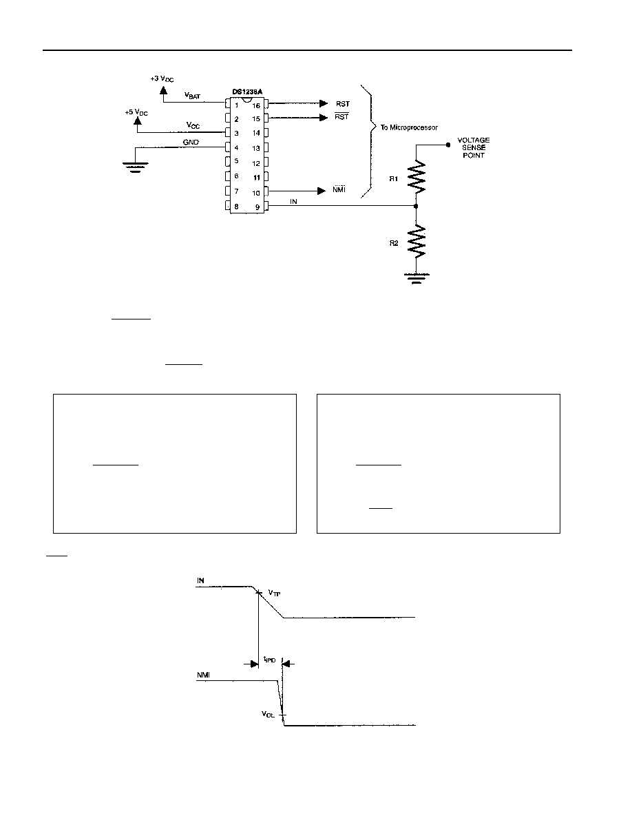
NON-MASKABLE INTERRUPT
The DS1238A generates a non-maskable interrupt (
NMI
) for early warning of a power failure to the
microprocessor. A precision comparator monitors the voltage level at the IN pin relative to an on-chip
reference generated by an internal band gap. The IN pin is a high-impedance input allowing for a user-
defined sense point. An external resistor voltage divider network (NO TAG) is used to interface with high
voltage signals. This sense point may be derived from the regulated 5-volt supply, or from a higher DC
voltage level closer to the main system power input. Since the IN trip point V
TP
is 1.27 volts, the proper
values for R1 and R2 can be determined by the equation as shown in NO TAG. Proper operation of the
DS1238A requires that the voltage at the IN pin be limited to V
IH
. Therefore, the maximum allowable
voltage at the supply being monitored (V
MAX
) can also be derived as shown in NO TAG. A simple
approach to solving this equation is to select a value for R2 of high enough value to keep power
consumption low, and solve for R1. The flexibility of the IN input pin allows for detection of power loss
at the earliest point in a power supply system, maximizing the amount of time for microprocessor
shutdown between
NMI
and RST or
RST
.
When the supply being monitored decays to the voltage sense point, the DS1238A will force the
NMI
output to an active state. Noise is removed from the
NMI
power-fail detection circuitry using built-in
time domain hysteresis. That is, the monitored supply is sampled periodically at a rate determined by an
internal ring oscillator running at approximately 30 kHz (33
µ
s/cycle). Three consecutive samplings of
out-of-tolerance supply (below V
SENSE
) must occur at the IN pin to active
NMI
. Therefore, the supply
must be below the voltage sense point for approximately 100
µ
s or the comparator will reset. In this way,
power supply noise is removed from the monitoring function preventing false trips. During a power-up,
any IN pin levels below V
TP
detected by the comparator are disabled from reaching the
NMI
pin until
V
CC
rises to V
CCTP
. As a result, any potential active
NMI
will not be initiated until V
CC
reaches V
CCTP
.
Removal of an active low level on the
NMI
pin is controlled by the subsequent rise of the IN pin above
V
TP
. The initiation and removal of the
NMI
signal during power up depends on the relative voltage
relationship between V
CC
and the IN pin voltage. Note that a fast-slewing power supply may cause the
NMI
to be virtually nonexistent on power-up. This is of no consequence, however, since an RST will be
active. The
NMI
voltage will follow V
CC
down until V
CC
decays to V
BAT
. Once V
CC
decays to V
BAT
, the
NMI
pin will enter a tri-state mode.
ST INPUT TIMING Figure 2
DS1238A
5 of 13
OSCILLATOR CONTROLS Table 1
Watchdog Timeout Period (typ)
OSCIN
OSCSEL
First Period
Following a Reset
Other Timeout
Reset Active
Duration
Ext Clk
Low
20480 Clks
5120 Clocks
641 Clks
Ext Cap
Low
pf
47
sec
2.2
X Cpf
pf
47
ms
550
X Cpf
pf
47
ms
69
X Cpf
Low
Hi/Open
2.7 sec
170 ms
85 ms
External
Internal
Hi/Open
Hi/Open
2.7 sec
2.7 sec
85 ms
Note that the OSCIN and OSCSEL pins are tri-stated when V
CC
is below V
BAT
.
POWER MONITOR, WATCHDOG TIMER, AND PUSHBUTTON RESET Figure 3
PUSHBUTTON RESET TIMING Figure 4
DS1238A
6 of 13
NON-MASKABLE INTERRUPT Figure 5
V
SENSE
=
R2
R2
R1
+
x 1.27
MAXVOLTAGE =
1.27
V
SENSE
x 5.0 = VMAX
Example 1: 5-Volt Supply, R2 = 10k Ohms,
V
SENSE
= 4.8 Volts
4.8 =
10k
10k
R1
+
x 1.27
R1 = 27.8k Ohm
Example 2: 12-Volt Supply, R2 = 10k Ohms,
V
SENSE
= 9.0 Volts
9.0 =
10k
10k
R1
+
x 1.27
R1 = 60.9k Ohm
V
MAX
=
1.27
9.00
x 5.0 = 35.4 Volts
NMI
FROM IN INPUT Figure 6

DS1238A
7 of 13
MEMORY BACKUP
The DS1238A provides all of the necessary functions required to battery back a static RAM. First, an
internal switch is provided to supply SRAM power from the primary 5-volt supply (V
CC
) or from an
external battery (V
BAT
), whichever is greater. Second, the same power-fail detection described in the
power monitor section is used to hold the chip enable output (
CEO
) to within 0.3 volts of V
CC
or to within
0.7 volts of V
BAT
. The output voltage diode drop from V
BAT
(0.7V) is necessary to prevent charging of the
battery in violation of UL standards. Write protection occurs as V
CC
falls below V
CCTP
as specified. If
CEI
is low at the time power-fail detection occurs,
CEO
is held in its present state until
CEI
is returned
high, or the period t
CE
expires. This delay of write protection until the current memory cycle is completed
prevents the corruption of data. If
CEO
is in an inactive state at the time of V
CC
fail detection,
CEO
will
be unconditionally disabled within t
CF
. During nominal supply conditions
CEO
will follow
CEI
with a
maximum propagation delay of 20 ns. NO TAG shows a typical nonvolatile SRAM application.
FRESHNESS SEAL
In order to conserve battery capacity during initial construction of an end system, the DS1238A provides
a freshness seal that electrically disconnects the battery. This means that upon battery attachment, the
V
CCO
output will remain inactive until V
CC
is applied. This prevents V
CCO
from powering other devices
when the battery is first attached, and V
CC
is not present. Once V
CC
is applied, the freshness seal is broken
and cannot be invoked again without subsequent removal and reattachment of the battery.
POWER SWITCHING
When larger operating currents are required in a battery-backed system, the internal switching devices of
the DS1238A may be too small to support the required load through V
CCO
with a reasonable voltage drop.
For these applications, the PF output is provided to gate external power switching devices. As shown in
Figure 8, power to the load is switched from V
CC
to battery on power-down, and from battery to V
CC
on
power-up. The DS1336 is designed to use the PF output to switch between V
BAT
and V
CC
. It provides
better leakage and switchover performance than currently available discrete components. The transition
threshold for PF is set to the external battery voltage V
BAT
, allowing a smooth transition between sources.
Any load applied to the PF pin by an external switch will be supplied by the battery. Therefore, if a
discrete switch is used, this load should be taken into consideration when sizing the battery.
NONVOLATILE SRAM Figure 7
DS1238A
8 of 13
POWER SWITCHING Figure 8
Note: If freshness on the DS1238A is not used,
PF
on the DS1336 may be tied to OUT1. This will free IN4, OUT4,
and V
BAT01
for system use.
TIMING DIAGRAMS
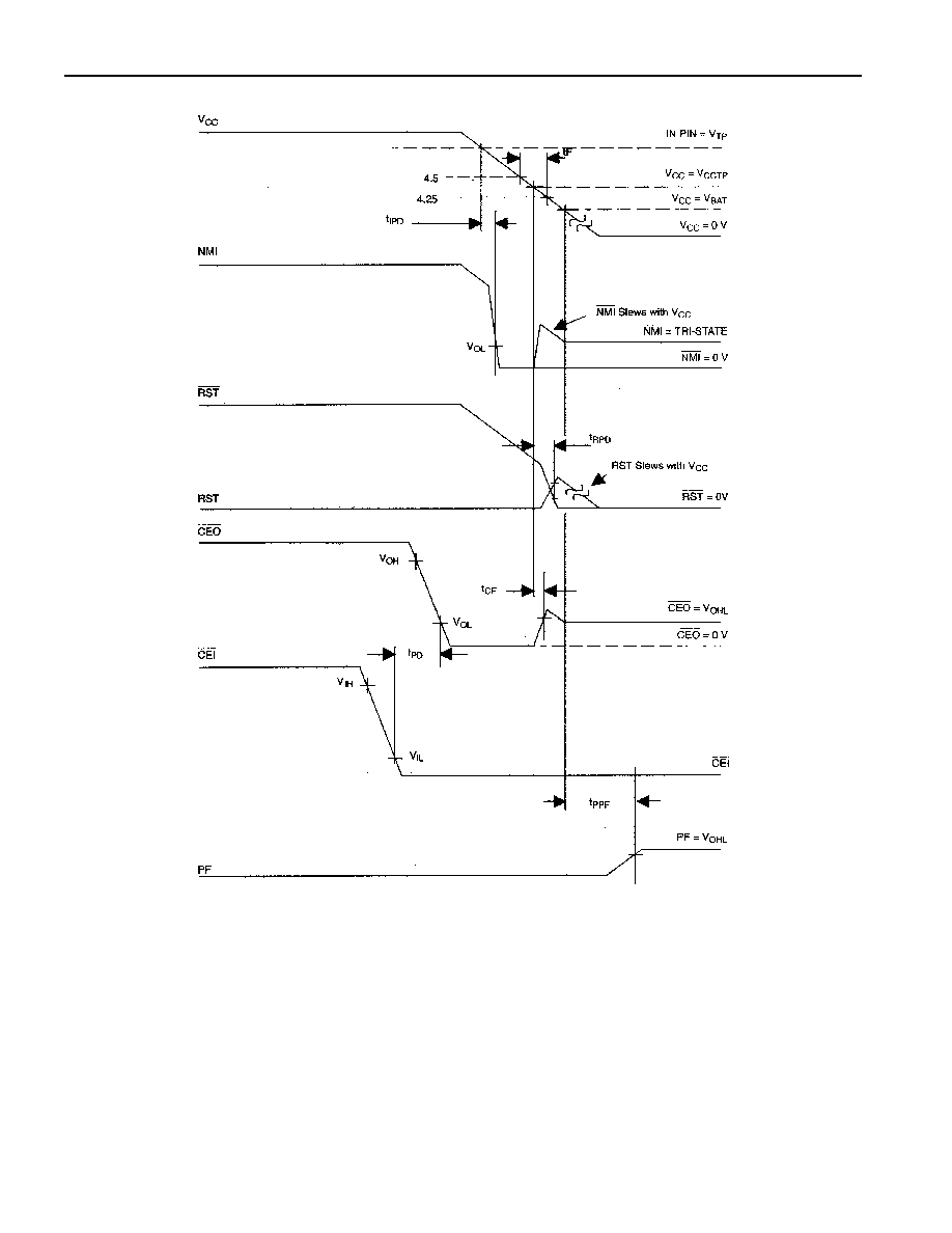
This section provides a description of the timing diagrams shown in Figure 9 and Figure 10. Figure 9
illustrates the relationship for power down. As V
CC
falls, the IN pin voltage drops below V
TP
. As a result,
the processor is notified of an impending power failure via an active
NMI
. This gives the processor time
to save critical data in nonvolatile SRAM. As the power falls further, V
CC
crosses V
CCTP
, the power
monitor trip point. When V
CC
reaches V
CCTP
, and active RST and
RST
are given. At this time,
CEO
is
brought high to write-protect the RAM. When the V
CC
reaches V
BAT
, a power-fail is issued via the PF
pin.
Figure 10 shows the power-up sequence. As V
CC
slews above V
BAT
, the PF pin is deactivated. An active
reset occurs as well as an
NMI
. Although the
NMI
may be short due to slew rates, reset will be
maintained for the standard t
RPU
timeout period . At a later time, if the IN pin falls below V
TP
, a new
NMI
will occur. If the processor does not issue an
ST
, a watchdog reset will also occur. The second
NMI
and
RST are provided to illustrate these possibilities.
DS1238A
9 of 13
POWER-DOWN TIMING Figure 9

DS1238A
10 of 13
POWER-UP TIMING Figure 10

DS1238A
11 of 13
ABSOLUTE MAXIMUM RATINGS*
Voltage on V
CC
Pin Relative to Ground
-0.5V to +7.0V
Voltage on I/O Relative to Ground
-0.5V to V
CC
+ 0.5V
Operating Temperature
0∞C to 70∞C
Operating Temperature (Industrial Version)
-40∞C to +85∞C
Storage Temperature
-55∞C to +125∞C
Soldering Temperature
260∞C for 10 seconds
*
This is a stress rating only and functional operation of the device at these or any other conditions
above those indicated in the operation sections of this specification is not implied. Exposure to
absolute maximum rating conditions for extended periods of time may affect reliability.
RECOMMENDED DC OPERATING CONDITIONS (0
∞
C to 70
∞
C)
PARAMETER
SYMBOL
MIN
TYP
MAX
UNITS NOTES
Supply Voltage
V
CC
4.5
5.0
5.5
V
1
Supply Voltage (5% Option)
V
CC
4.75
5.0
5.5
V
1
Input High Level
V
IH
2.0
V
CC
+0.3
V
1
Input Low Level
V
IL
-0.3
+0.8
V
1
IN Input Pin
V
IN
0
V
CC
V
1
Battery Input
V
BAT
0
4.0
V
1
DC ELECTRICAL CHARACTERISTICS (0
∞
C to 70
∞
C; V
DD
= 5V
±
10%)
PARAMETER
SYMBOL
MIN
TYP
MAX
UNITS NOTES
Supply Current
I
CC
4
mA
2
Battery Current
I
BAT
0
200
nA
2, 12
Supply Output Current
(V
CCO
= V
CC
- 0.3V)
I
CC01
100
mA
3
Supply Out Current (V
CC
< V
BAT
)
I
CC02
1
mA
4
Supply Output Voltage
V
CCO
V
CC
-0.3
V
1
Battery Back Voltage
V
CCO
V
BAT
-0.8
V
6
Low Level @ RST
V
OL
0.4
V
1
Output Voltage @ -500
µ
A
V
OH
V
CC
-0.5V V
CC
-0.1V
V
1
CEO
and PF Output
V
OHL
V
BAT
-0.8
V
6
Input Leakage Current
I
LI
-1.0
+1.0
µ
A
2
Output Leakage Current
I
LO
-1.0
+1.0
µ
A
11
Output Current @ 0.4V
I
OL
4.0
mA
9
Output Current @ 2.4V
I
OH
-1.0
mA
10
Power Sup. Trip Point
V
CCTP
4.25
4.37
4.50
V
1
Power Supply Trip (5% Option)
V
CCTP
4.50
4.62
4.75
V
IN Input Pin Current
I
CCIN
-1.0
+1.0
µ
A
IN Input Trip Point
V
TP
1.15
1.27
1.35
V
1

DS1238A
12 of 13
AC ELECTRICAL CHARACTERISTICS (0
∞
C to 70
∞
C; V
CC
= 5V
±
10%)
PARAMETER
SYMBOL
MIN
TYP
MAX
UNITS NOTES
V
CC
Fail Detect to RST,
RST
t
RPD
40
100
175
µ
s
V
TP
to
NMI
t
IPD
40
100
175
µ
s
RESET Active OSCSEL=high
t
RST
40
85
150
ms
ST
Pulse Width
t
ST
20
ns
13
PBRST @ V
IL
t
PB
30
ms
V
CC
Slew Rate 4.75 to 4.25
t
F
300
µ
s
Chip Enable Prop Delay
t
PD
20
ns
V
CC
Fail to Chip Enable High
t
CF
7
12
144
µ
s
11
V
CC
Valid to RST (RC=1)
t
FPU
100
ns
V
CC
Valid to RST
t
RPU
40
100
150
ms
5
V
CC
Slew to 4.25 to V
BAT
t
FB1
10
µ
s
Chip Enable Output Recovery
Time
t
REC
0.1
µ
s
7
V
CC
Slew 4.25 to 4.75
t
R
0
µ
s
Chip Enable Pulse Width
t
CE
5
µ
s
8
Watchdog Time Delay Int Clock
Long period
t
TD
1.7
2.7
s
Short period
110
170
ms
Watchdog Time Delay, Ext
Clock, after Reset
t
TD
20480
clocks
Normal
5120
clocks
V
BAT
Detect to PF
t
PPF
2
µ
s
OSC IN Frequency
f
OSC
0
250
kHz
CAPACITANCE (t
A
=25
∞
C)
PARAMETER
SYMBOL
MIN
TYP
MAX
UNITS NOTES
Input Capacitance
C
IN
5
pF
Output Capacitance
C
OUT
7
pF
DS1238A
13 of 13
NOTES:
1.
All voltages referenced to ground.
2.
Measured with V
CCO
,
CEO
, PF,
ST
, RST,
RST
, and
NMI
pin open.
3.
I
CCO1
is the maximum average load which the DS1238A can supply at V
CC
-.3V through the V
CCO
pin
during normal 5-volt operation.
4.
I
CCO2
is the maximum average load which the DS1238A can supply through the V
CCO
pin during data
retention battery supply operation, with a maximum drop of 0.8 volts for commercial, 1.0V for
industrial.
5.
With t
R
= 5
µ
s.
6.
V
CCO
is approximately V
BAT
-0.5V at 1
µ
A load.
7.
t
REC
is the minimum time required before
CEI
/
CEO
memory access is allowed.
8.
t
CE
maximum must be met to insure data integrity on power loss.
9.
All outputs except RST which is 25
µ
A max.
10.
All outputs except
RST
,
RTV
, and
NMI
which is 25
µ
A min.
11.
The
ST
pin will sink
±
50
µ
A in normal operation. The OSCIN pin will sink
±
5
µ
A in normal
operation. The OSCSEL pin will sink
±
10
µ
A in normal operation.
12.
I
BAT
is measured with V
BAT
=3.0V.
13.
ST
should be active low before the watchdog is disabled (i.e., before the
ST
input is tristated).