 | –≠–ª–µ–∫—Ç—Ä–æ–Ω–Ω—ã–π –∫–æ–º–ø–æ–Ω–µ–Ω—Ç: DS1306 | –°–∫–∞—á–∞—Ç—å:  PDF PDF  ZIP ZIP |
1 of 20
070900
FEATURES
Real time clock counts seconds, minutes,
hours, date of the month, month, day of the
week, and year with leap year compensation
valid up to 2100
96-byte nonvolatile RAM for data storage
Two Time of Day Alarms - programmable on
combination of seconds, minutes, hours, and
day of the week
1 Hz and 32.768 kHz clock outputs
Serial interface supports Motorola Serial
Peripheral Interface (SPI) serial data ports or
standard 3-wire interface
Burst Mode for reading/writing successive
addresses in clock/RAM
Dual power supply pins for primary and
backup power supplies
Optional trickle charge output to backup
supply
2.0 - 5.5V operation
Optional industrial temperature range
-40∞C to +85∞C
Available in space-efficient 20-pin TSSOP
package
Recognized by Underwriters Laboratory
ORDERING INFORMATION
DS1306 16-Pin
DIP
DS1306N
16-Pin DIP (Industrial)
DS1306E 20-Pin
TSSOP
DS1306EN
20-Pin TSSOP (Industrial)
PIN ASSIGNMENT
PIN DESCRIPTION
V
CC1
≠ Primary Power Supply
V
CC2
≠ Backup Power Supply
V
BAT
≠ +3V Battery Input
V
CCIF
≠ Interface Logic Power Supply
Input
GND ≠
Ground
X1, X2
≠ 32.768 kHz Crystal Connection
INT0
≠ Interrupt 0 Output
INT1
≠ Interrupt 1 Output
SDI
≠ Serial Data In
SDO
≠ Serial Data Out
CE
≠ Chip Enable
SCLK
≠ Serial Clock
SERMODE ≠ Serial Interface Mode
1 Hz
- 1 Hz Output
32 kHz
- 32.768 kHz Output
DS1306
Serial Alarm Real Time Clock (RTC)
www.dalsemi.com
DS1306 20-Pin TSSOP (173 mil)
V
CC2
V
BAT
X1
NC
X2
NC
INT0
INT1
1 Hz
GND
V
CC1
NC
32 kHz
V
CCIF
SDO
SDI
SCLK
NC
CE
SERMODE
20
19
18
17
16
15
14
13
12
11
1
2
3
4
5
6
7
8
9
10
V
CC2
DS1306 16-Pin DIP (300 mil)
15
X1
INT0
1 Hz
GND
V
CC1
SDO
SDI
SCLK
CE
SERMODE
1
2
3
4
5
6
7
8
16
14
13
12
11
10
9
V
BAT
X2
INT1
32 kHz
V
CCIF
DS1306
2 of 20
DESCRIPTION
The DS1306 Serial Alarm Real Time Clock provides a full BCD clock calendar which is accessed via a
simple serial interface. The clock/calendar provides seconds, minutes, hours, day, date, month, and year
information. The end of the month date is automatically adjusted for months with less than 31 days,
including corrections for leap year. The clock operates in either the 24-hour or 12-hour format with
AM/PM indicator. In addition 96 bytes of nonvolatile RAM are provided for data storage.
An interface logic power supply input pin (V
CCIF
) allows the DS1306 to drive SDO and 32 kHz pins to a
level that is compatible with the interface logic. This allows an easy interface to 3-volt logic in mixed
supply systems. The DS1306 offers dual power supplies as well as a battery input pin. The dual power
supplies support a programmable trickle charge circuit which allows a rechargeable energy source (such
as a super cap or rechargeable battery) to be used for a backup supply. The V
BAT
pin allows the device to
be backed up by a non-rechargeable battery. The DS1306 is fully operational from 2.0 to 5.5 volts.
Two programmable time of day alarms are provided by the DS1306. Each alarm can generate an
interrupt on a programmable combination of seconds, minutes, hours, and day. "Don't care" states can be
inserted into one or more fields if it is desired for them to be ignored for the alarm condition. A 1 Hz and
a 32 kHz clock output are also available.
The DS1306 supports a direct interface to Motorola SPI serial data ports or standard 3-wire interface. An
easy-to-use address and data format is implemented in which data transfers can occur 1 byte at a time or
in multiple-byte burst mode.
OPERATION
The block diagram in Figure 1 shows the main elements of the Serial Alarm RTC. The following
paragraphs describe the function of each pin.
DS1306 BLOCK DIAGRAM Figure 1

DS1306
3 of 20
SIGNAL DESCRIPTIONS
V
CC1
- DC power is provided to the device on this pin. V
CC1
is the primary power supply.
V
CC2
- This is the secondary power supply pin. In systems using the trickle charger, the rechargeable
energy source is connected to this pin.
V
BAT
- Battery input for any standard 3-volt lithium cell or other energy source.
V
CCIF
(Interface Logic Power Supply Input) - The V
CCIF
pin allows the DS1306 to drive SDO and
32 kHz output pins to a level that is compatible with the interface logic, thus allowing an easy interface to
3-volt logic in mixed supply systems. This pin is physically connected to the source connection of the p-
channel transistors in the output buffers of the SDO and 32 kHz pins.
SERMODE (Serial Interface Mode Input) - The SERMODE pin offers the flexibility to choose
between two serial interface modes. When connected to GND, standard 3-wire communication is
selected. When connected to V
CC
, Motorola SPI communication is selected.
SCLK (Serial Clock Input) - SCLK is used to synchronize data movement on the serial interface for
either the SPI or 3-wire interface.
SDI (Serial Data Input) - When SPI communication is selected, the SDI pin is the serial data input for
the SPI bus. When 3-wire communication is selected, this pin must be tied to the SDO pin (the SDI and
SDO pins function as a single I/O pin when tied together).
SDO (Serial Data Output) - When SPI communication is selected, the SDO pin is the serial data output
for the SPI bus. When 3-wire communication is selected, this pin must be tied to the SDI pin (the SDI
and SDO pins function as a single I/O pin when tied together).
CE (Chip Enable) - The Chip Enable signal must be asserted high during a read or a write for both
3-wire and SPI communication. This pin has an internal 55k pull-down resistor (typical).
INT0
(Interrupt 0 Output) - The
INT0
pin is an active low output of the DS1306 that can be used as an
interrupt input to a processor. The
INT0
pin can be programmed to be asserted by Alarm 0. The
INT0
pin remains low as long as the status bit causing the interrupt is present and the corresponding interrupt
enable bit is set. The
INT0
pin operates when the DS1306 is powered by V
CC1
, V
CC2
, or V
BAT
. The
INT0
pin is an open drain output and requires an external pullup resistor.
1 Hz (1 Hz Clock Output) - The 1 Hz pin provides a 1 Hz squarewave output. This output is active
when the 1 Hz bit in the control register is a logic 1.
Both
INT0
and 1 Hz pins are open drain outputs. The interrupt, 1 Hz signal, and the internal clock
continue to run regardless of the level of V
CC
(as long as a power source is present).
INT1 (Interrupt 1 Output) - The INT1 pin is an active high output of the DS1306 that can be used as an
interrupt input to a processor. The INT1 pin can be programmed to be asserted by alarm 1. When an
alarm condition is present, the INT1 pin generates a 62.5 ms active high pulse. The INT1 pin operates
only when the DS1306 is powered by V
CC2
or V
BAT
. When active, the INT1 pin is internally pulled up to
V
CC2
or V
BAT
. When inactive, the INT1 pin is internally pulled low.

DS1306
4 of 20
32 kHz (32.768 kHz Clock Output) - The 32 kHz pin provides a 32.768 kHz output. This signal is
always present.
X1, X2 - Connections for a standard 32.768 kHz quartz crystal. The internal oscillator is designed for
operation with a crystal having a specified load capacitance of 6 pF. For more information on crystal
selection and crystal layout considerations, please consult Application Note 58, "Crystal Considerations
with Dallas Real Time Clocks." The DS1306 can also be driven by an external 32.768 kHz oscillator. In
this configuration, the X1 pin is connected to the external oscillator signal and the X2 pin is floated.
RTC AND RAM ADDRESS MAP
The address map for the RTC and RAM registers of the DS1306 is shown in Figure 2. Data is written to
the RTC by writing to address locations 80h to 9Fh and is written to the RAM by writing to address
locations A0h to FFh. RTC data is read by reading address locations 00h to 1Fh and RAM data is read by
reading address locations 20h to 7Fh.
ADDRESS MAP Figure 2
00H
1FH
CLOCK/CALENDAR
READ ADDRESSES ONLY
20H
7FH
96-BYTES USER RAM
READ ADDRESSES ONLY
80H
9FH
CLOCK/CALENDAR
WRITE ADDRESSES ONLY
A0H
FFH
96-BYTES USER RAM
WRITE ADDRESSES ONLY
DS1306
5 of 20
CLOCK, CALENDAR, AND ALARM
The time and calendar information is obtained by reading the appropriate register bytes. The real time
clock registers are illustrated in Figure 3. The time, calendar, and alarm are set or initialized by writing
the appropriate register bytes. Note that some bits are set to 0. These bits will always read 0 regardless
of how they are written. Also note that registers 12h to 1Fh (read) and registers 92h to 9Fh are reserved.
These registers will always read 0 regardless of how they are written. The contents of the time, calendar,
and alarm registers are in the Binary-Coded Decimal (BCD) format.
RTC REGISTERS Figure 3
RTC REGISTERS DS1306
HEX ADDRESS
READ WRITE
Bit7
Bit6
Bit5
Bit4
Bit3
Bit2
Bit1
Bit0
RANGE
00H
80H
0
10 SEC
SEC
00-59
01H
81H
0
10 MIN
MIN
00-59
10
01-12 + P/A
02H
82H
0
12/2
4
P/A
10 HR
HOURS
00-23
03H
83H
0
0
0
0
0
DAY
01-07
04H
84H
0
0
10 DATE
DATE
1-31
05H
85H
0
0
10 MONTH
MONTH
01-12
06H
86H
10 YEAR
YEAR
00-99
Alarm 0
07H
87H
M
10 SEC ALARM
SEC ALARM
00-59
08H
88H
M
10 MIN ALARM
MIN ALARM
00-59
10
01-12 + P/A
09H
89H
M
12/2
4
P/A
10 HR
HOUR ALARM
00-23
0AH
8AH
M
0
0
0
0
DAY ALARM
01-07
Alarm 1
0BH
8BH
M
10 SEC ALARM
SEC ALARM
00-59
0CH
8CH
M
10 MIN ALARM
MIN ALARM
00-59
10
01-12 + P/A
0DH
8DH
M
12/2
4
P/A
10 HR
HOUR ALARM
00-23
0EH
8EH
M
0
0
0
0
DAY ALARM
01-07
0FH
8FH
CONTROL REGISTER
10H
90H
STATUS REGISTER
11H
91H
TRICKLE CHARGER REGISTER
12-1FH
92-9FH
RESERVED
NOTE:
Range for alarm registers does not include mask'm' bits.
DS1306
6 of 20
The DS1306 can be run in either 12-hour or 24-hour mode. Bit 6 of the hours register is defined as the
12- or 24-hour mode select bit. When high, the 12-hour mode is selected. In the 12-hour mode, bit 5 is
the AM/PM bit with logic high being PM. In the 24-hour mode, bit 5 is the second 10-hour bit (20-23
hours).
The DS1306 contains two time of day alarms. Time of Day Alarm 0 can be set by writing to registers
87h to 8Ah. Time of Day Alarm 1 can be set by writing to registers 8Bh to 8Eh. Bit 7 of each of the time
of day alarm registers are mask bits (Table 1). When all of the mask bits are logic 0, a time of day alarm
will only occur once per week when the values stored in timekeeping registers 00h to 03h match the
values stored in the time of day alarm registers. An alarm will be generated every day when bit 7 of the
day alarm register is set to a logic 1. An alarm will be generated every hour when bit 7 of the day and
hour alarm registers is set to a logic 1. Similarly, an alarm will be generated every minute when bit 7 of
the day, hour, and minute alarm registers is set to a logic 1. When bit 7 of the day, hour, minute, and
seconds alarm registers is set to a logic 1, an alarm will occur every second.
TIME OF DAY ALARM MASK BITS Table 1
ALARM REGISTER MASK BITS (BIT 7)
SECONDS MINUTES
HOURS
DAYS
1
1
1
1
Alarm once per second
0
1
1
1
Alarm when seconds match
0
0
1
1
Alarm when minutes and seconds match
0
0
0
1
Alarm when hours, minutes, and seconds match
0
0
0
0
Alarm when day, hours, minutes, and seconds
match
SPECIAL PURPOSE REGISTERS
The DS1306 has three additional registers (Control Register, Status Register, and Trickle Charger
Register) that control the real time clock, interrupts, and trickle charger.
CONTROL REGISTER (READ 0FH, WRITE 8FH)
BIT7
BIT6
BIT5
BIT4
BIT3
BIT2
BIT1
BIT0
0
WP
0
0
0
1 Hz
AIE1
AIE0
WP (Write Protect) - Before any write operation to the clock or RAM, this bit must be logic 0. When
high, the write protect bit prevents a write operation to any register, including bits 0, 1, and 2 of the
control register. Upon initial power up, the state of the WP bit is undefined. Therefore the WP bit should
be cleared before attempting to write to the device.
1 Hz (1 Hz output enable) - This bit controls the 1 Hz output. When this bit is a logic 1, the 1 Hz output
is enabled. When this bit is a logic 0, the 1 Hz output is high Z.
AIE0 (Alarm Interrupt Enable 0) - When set to a logic 1, this bit permits the Interrupt 0 Request Flag
(IRQF0) bit in the status register to assert
INT0
. When the AIE0 bit is set to logic 0, the IRQF0 bit does
not initiate the
INT0
signal.
AIE1 (Alarm Interrupt Enable 1) - When set to a logic 1, this bit permits the Interrupt 1 Request Flag
(IRQF1) bit in the status register to assert INT1. When the AIE1 bit is set to logic 0, the IRQF1 bit does
not initiate an interrupt signal, and the INT1 pin is set to a logic 0 state.

DS1306
7 of 20
STATUS REGISTER (READ 10H)
BIT7
BIT6
BIT5
BIT4
BIT3
BIT2
BIT1
BIT0
0
0
0
0
0
0
IRQF1
IRQF0
IRQF0 (Interrupt 0 Request Flag) - A logic 1 in the Interrupt Request Flag bit indicates that the current
time has matched the Alarm 0 registers. If the AIE0 bit is also a logic 1, the
INT0
pin will go low.
IRQF0 is cleared when any of the Alarm 0 registers are read or written.
IRQF1 (Interrupt 1 Request Flag) - A logic 1 in the Interrupt Request Flag bit indicates that the current
time has matched the Alarm 1 registers. If the AIE1 bit is also a logic 1, the INT1 pin will generate a
62.5- ms active high pulse. IRQF1 is cleared when any of the Alarm 1 registers are read or written.
TRICKLE CHARGE REGISTER (READ 11H, WRITE 91H)
This register controls the trickle charge characteristics of the DS1306. The simplified schematic of
Figure 4 shows the basic components of the trickle charger. The trickle charge select (TCS) bits (bits
4-7) control the selection of the trickle charger. In order to prevent accidental enabling, only a pattern of
1010 will enable the trickle charger. All other patterns will disable the trickle charger. The DS1306
powers up with the trickle charger disabled. The diode select (DS) bits (bits 2-3) select whether one
diode or two diodes are connected between V
CC1
and V
CC2
. If DS is 01, one diode is selected. If DS is
10, two diodes are selected. If DS is 00 or 11, the trickle charger is disabled independently of TCS. The
RS bits select the resistor that is connected between V
CC1
and V
CC2
. The resistor is selected by the
resistor select (RS) bits as shown in Table 2.
PROGRAMMABLE TRICKLE CHARGER Figure 4

DS1306
8 of 20
TRICKLE CHARGER RESISTOR SELECT Table 2
RS BITS
RESISTOR
TYPICAL VALUE
00
None
None
01
R1
2 k
10
R2
4 k
11
R3
8 k
If RS is 00, the trickle charger is disabled independently of TCS.
Diode and resistor selection is determined by the user according to the maximum current desired for
battery or super cap charging. The maximum charging current can be calculated as illustrated in the
following example. Assume that a system power supply of 5 volts is applied to V
CC1
and a super cap is
connected to V
CC2
. Also assume that the trickle charger has been enabled with one diode and resister R1
between V
CC1
and V
CC2
. The maximum current I MAX would therefore be calculated as follows:
I
MAX
= (5.0V - diode drop)/R1
~ (5.0V - 0.7V)/2 k
~ 2.2 mA
Obviously, as the super cap charges, the voltage drop between V
CC1
and V
CC2
will decrease and therefore
the charge current will decrease.
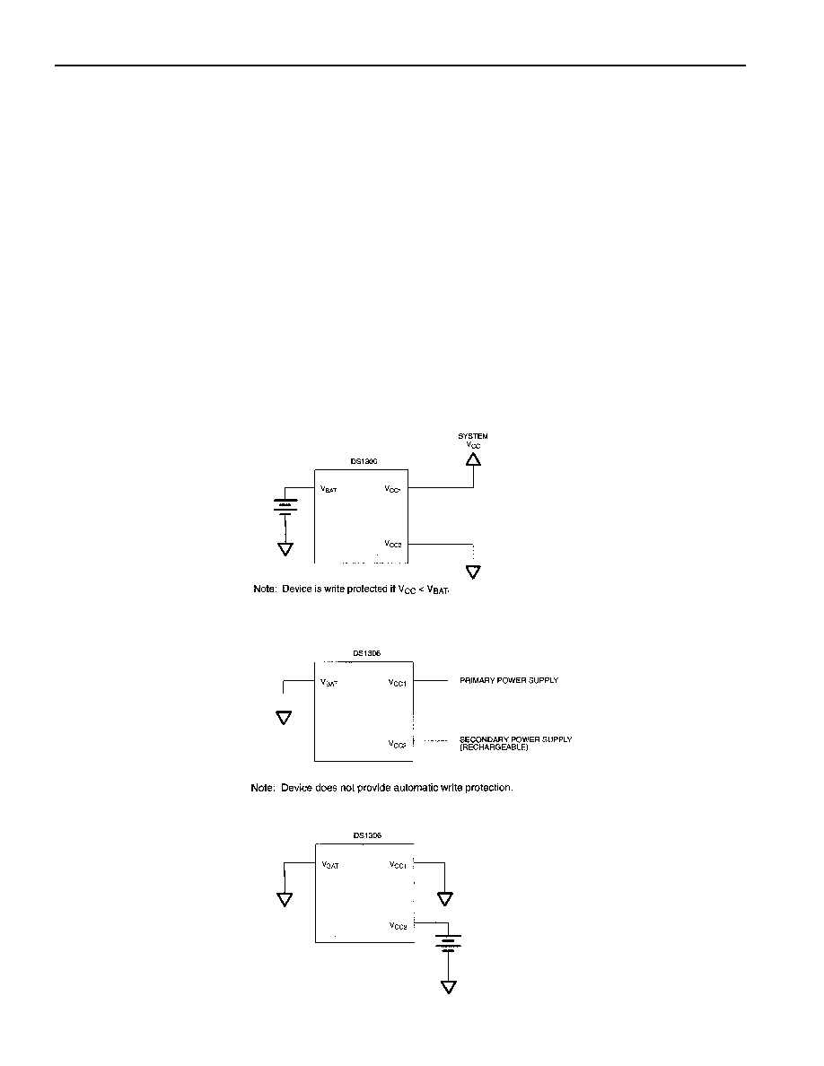
POWER CONTROL
Power is provided through the V
CC1
, V
CC2
, and V
BAT
pins. Three different power supply configurations
are illustrated in Figure 5. Configuration 1 shows the DS1306 being backed up by a non-rechargeable
energy source such as a lithium battery. In this configuration, the system power supply is connected to
V
CC1
and V
CC2
is grounded. The DS1306 will be write-protected if V
CC1
is less than V
BAT
.
Configuration 2 illustrates the DS1306 being backed up by a rechargeable energy source. In this case, the
V
BAT
pin is grounded, V
CC1
is connected to the primary power supply, and V
CC2
is connected to the
secondary supply (the rechargeable energy source). The DS1306 will operate from the larger of V
CC1
or
V
CC2
. When V
CC1
is greater than V
CC2
+ 0.2 volt (typical), V
CC1
will power the DS1306. When V
CC1
is
less than V
CC2
, V
CC2
will power the DS1306. The DS1306 does not write-protect itself in this
configuration.
Configuration 3 shows the DS1306 in battery operate mode where the device is powered only by a single
battery. In this case, the V
CC1
and V
BAT
pins are grounded and the battery is connected to the V
CC2
pin.
Only these three configurations are allowed. Unused supply pins must be grounded.
SERIAL INTERFACE
The DS1306 offers the flexibility to choose between two serial interface modes. The DS1306 can
communicate with the SPI interface or with a standard 3-wire interface. The interface method used is
determined by the SERMODE pin. When this pin is connected to V
CC
, SPI communication is selected.
When this pin is connected to ground, standard 3-wire communication is selected.
SERIAL PERIPHERAL INTERFACE (SPI)
The serial peripheral interface (SPI) is a synchronous bus for address and data transfer and is used when
interfacing with the SPI bus on specific Motorola microcontrollers such as the 68HC05C4 and the
68HC11A8. The SPI mode of serial communication is selected by tying the SERMODE pin to V
CC
.
DS1306
9 of 20
Four pins are used for the SPI. The four pins are the SDO (Serial Data Out), SDI (Serial Data In), CE
(Chip Enable), and SCLK (Serial Clock). The DS1306 is the slave device in an SPI application, with the
microcontroller being the master.
The SDI and SDO pins are the serial data input and output pins for the DS1306, respectively. The CE
input is used to initiate and terminate a data transfer. The SCLK pin is used to synchronize data
movement between the master (microcontroller) and the slave (DS1306) devices.
The shift clock (SCLK), which is generated by the microcontroller, is active only during address and data
transfer to any device on the SPI bus. The inactive clock polarity is programmable in some
microcontrollers. The DS1306 offers an important feature in that the level of the inactive clock is
determined by sampling SCLK when CE becomes active. Therefore either SCLK polarity can be
accommodated. Input data (SDI) is latched on the internal strobe edge and output data (SDO) is shifted
out on the shift edge (see Table 3 and Figure 6). There is one clock for each bit transferred. Address and
data bits are transferred in groups of eight.
POWER SUPPLY CONFIGURATIONS FOR THE DS1306 Figure 5
Configuration 1: Backup Supply is a Non-Rechargeable Lithium Battery
Configuration 2: Backup Supply is a Rechargeable Battery or Super Capacitor
Configuration 3: Battery Operate Mode

DS1306
10 of 20
FUNCTION TABLE Table 3
MODE
CE
SCLK
SDI
SDO
Disable Reset
L
Input Disabled
Input Disabled
High Z
Write
H
CPOL=1*
CPOL=0
Data Bit Latch
High Z
Read
H
CPOL=1
CPOL=0
X
Next data bit
shift**
* CPOL is the "Clock Polarity" bit that is set in the control register of the microcontroller.
** SDO remains at High Z until 8 bits of data are ready to be shifted out during a read.
NOTE:
CPHA bit polarity (if applicable) may need to be set accordingly.
SERIAL CLOCK AS A FUNCTION OF MICROCONTROLLER
CLOCK POLARITY (CPOL) Figure 6

DS1306
11 of 20
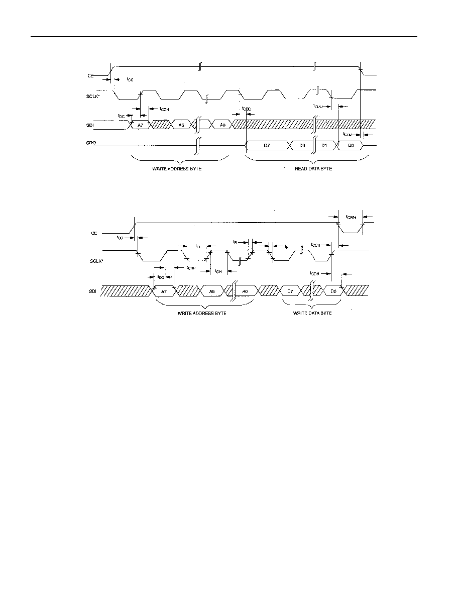
ADDRESS AND DATA BYTES
Address and data bytes are shifted MSB first into the serial data input (SDI) and out of the serial data
output (SDO). Any transfer requires the address of the byte to specify a write or read to either a RTC or
RAM location, followed by 1 or more bytes of data. Data is transferred out of the SDO for a read
operation and into the SDI for a write operation (see figures 7 and 8).
SPI SINGLE-BYTE WRITE Figure 7
SPI SINGLE-BYTE READ Figure 8
* SCLK can be either polarity.
The address byte is always the first byte entered after CE is driven high. The most significant bit (A7) of
this byte determines if a read or write will take place. If A7 is 0, one or more read cycles will occur. If
A7 is 1, one or more write cycles will occur.
Data transfers can occur 1 byte at a time or in multiple-byte burst mode. After CE is driven high an
address is written to the DS1306. After the address, 1 or more data bytes can be written or read. For a
single-byte transfer 1 byte is read or written and then CE is driven low. For a multiple-byte transfer,
however, multiple bytes can be read or written to the DS1306 after the address has been written. Each
read or write cycle causes the RTC register or RAM address to automatically increment. Incrementing
continues until the device is disabled. When the RTC is selected, the address wraps to 00h after
incrementing to 1Fh (during a read) and wraps to 80h after incrementing to 9Fh (during a write). When
the RAM is selected, the address wraps to 20h after incrementing to 7Fh (during a read) and wraps to
A0h after incrementing to FFh (during a write).

DS1306
12 of 20
SPI MULTIPLE-BYTE BURST TRANSFER Figure 9
3-WIRE INTERFACE
The 3-wire interface mode operates similar to the SPI mode. However, in 3-wire mode there is one I/O
instead of separate data in and data out signals. The 3-wire interface consists of the I/O (SDI and SDO
pins tied together), CE, and SCLK pins. In 3-wire mode, each byte is shifted in LSB first unlike SPI
mode where each byte is shifted in MSB first.
As is the case with the SPI mode, an address byte is written to the device followed by a single data byte
or multiple data bytes. Figure 10 illustrates a read and write cycle. In 3-wire mode, data is input on the
rising edge of SCLK and output on the falling edge of SCLK.
3-WIRE SINGLE BYTE TRANSFER Figure 10
SINGLE BYTE READ
SINGLE BYTE WRITE
I/O is SDI and SDO tied together
In burst mode, RST is kept high and additional SCLK cycles are sent until the end of the burst.
RST
SCLK
I/O
A0 A1
A2
A3 A4
A5 A6 A7
RST
SCLK
I/O
D0
D1
D2
D3
D4 D5 D6 D7
A0 A1
A2
A3
A4
A5 A6 A7

DS1306
13 of 20
ABSOLUTE MAXIMUM RATINGS*
Voltage on Any Pin Relative to Ground
-0.5V to +7.0V
Operating Temperature
0
∞
C to 70
∞
C or ≠40∞C to +85∞C for Industrial (IND)
Storage Temperature
-55
∞
C to +125
∞
C
Soldering Temperature
260
∞
C for 10 seconds (DIP)
See IPC/JEDEC Standard J-STD-020A for
Surface Mount Devices
* This is a stress rating only and functional operation of the device at these or any other conditions above
those indicated in the operation sections of this specification is not implied. Exposure to absolute
maximum rating conditions for extended periods of time may affect reliability.
RECOMMENDED DC OPERATING CONDITIONS
(0
∞
C to 70
∞
C or ≠40∞ to +85∞C)
PARAMETER
SYMBOL
MIN TYP
MAX
UNITS NOTES
Supply Voltage V
CC1
, V
CC2
V
CC1
,
V
CC2
2.0
5.5
V
1, 8
Logic 1 Input
V
IH
2.0
V
CC
+0.3
V
1
V
CC
=2.0V
-0.3
+0.3
Logic 0 Input
V
IL
V
CC
=5V
-0.3
+0.8
V
1
V
BAT
Battery Voltage
V
BAT
2.0
5.5
V
1
V
CCIF
Supply Voltage
V
CCIF
2.0
5.5
V
14
DC ELECTRICAL CHARACTERISTICS
(0
∞
C to 70
∞
C or ≠40∞C to +85∞C; V
CC
= 2.0 to 5.5V*)
PARAMETER
SYMBOL
MIN TYP
MAX
UNITS NOTES
Input Leakage
I
LI
-100
+500
µ
A
Output Leakage
I
LO
-1
1
µ
A
V
CC
=2.0
0.4
Logic 0 Output
V
OL
V
CC
=5V
0.4
V
2
V
CCIF
=2.0V
1.6
Logic 1 Output
V
OH
V
CCIF
=5V
2.4
V
12
Logic 1 Output Current (INT1 pin)
I
OH
,
INT1
(V
CC2
, V
BAT
)
-0.3V
-100
µ
A
V
CC1
=2.0V
0.425
V
CC1
Active Supply Current
I
CC1A
V
CC1
=5V
1.28
mA
4, 9
V
CC1
=2.0V
25.3
V
CC1
Timekeeping Current
I
CC1T
V
CC1
=5V
81
µ
A
3,9
V
CC2
=2.0V
0.4
V
CC2
Active Supply Current
I
CC2A
V
CC2
=5V
1.2
mA
4, 10
V
CC2
=2.0V
0.4
V
CC2
Timekeeping Current
I
CC2T
V
CC2
=5V
1
µ
A
3, 10
*Unless otherwise noted.
DS1306
14 of 20
DC ELECTRICAL CHARACTERISTICS (cont'd)
(0
∞
C to 70
∞
C or ≠40∞C to +85∞C; V
CC
= 2.0 to 5.5V*)
PARAMETER
SYMBOL
MIN TYP
MAX
UNITS NOTES
Battery Timekeeping Current
I
BATT
V
BAT
=3V
550
nA
12
Battery Timekeeping Current
(IND)
I
BATT
V
BAT
=3V
800
nA
12
Trickle Charge Resistors
R1
R2
R3
2
4
8
k
k
k
Trickle Charger Diode Voltage
Drop
V
TD
0.7
V
CAPACITANCE (t
A
= 25
∞
C)
PARAMETER
SYMBOL CONDITION
TYP
MAX
UNITS NOTES
Input Capacitance
C
I
10
pF
Output Capacitance
C
O
15
pF
Crystal Capacitance
C
X
6
pF
3-WIRE AC ELECTRICAL CHARACTERISTICS
(0
∞
C to 70
∞
C or ≠40∞C to +85∞C; V
CC
= 2.0V to 5.5V*)
PARAMETER
SYMBOL
MIN TYP
MAX
UNITS NOTES
V
CC
=2.0V
200
Data to CLK Setup
t
DC
V
CC
=5V
50
ns
5, 6
V
CC
=2.0V
280
CLK to Data Hold
t
CDH
V
CC
=5V
70
ns
5, 6
V
CC
=2.0V
800
CLK to Data Delay
t
CDD
V
CC
=5V
200
ns
5, 6, 7
V
CC
=2.0V
1000
CLK Low Time
t
CL
V
CC
=5V
250
ns
6
V
CC
=2.0V
1000
CLK High Time
t
CH
V
CC
=5V
250
ns
6
V
CC
=2.0V
0.6
CLK Frequency
t
CLK
V
CC
=5V
DC
2.0
MHz
6
V
CC
=2.0V
2000
CLK Rise and Fall
t
R
, t
F
V
CC
=5V
500
ns
V
CC
=2.0V
4
CE to CLK Setup
t
CC
V
CC
=5V
1
µ
s
6
V
CC
=2.0V
240
CLK to CE Hold
t
CCH
V
CC
=5V
60
ns
6
V
CC
=2.0V
4
CE Inactive Time
t
CWH
V
CC
=5V
1
µ
s
6
V
CC
=2.0V
280
CE to Output High Z
t
CDZ
V
CC
=5V
70
ns
5, 6
V
CC
=2.0V
280
SCLK to Output High Z
t
CCZ
V
CC
=5V
70
ns
5, 6
*Unless otherwise noted.
DS1306
15 of 20
TIMING DIAGRAM: 3-WIRE READ DATA TRANSFER Figure 12
TIMING DIAGRAM: 3-WIRE WRITE DATA TRANSFER Figure 13

DS1306
16 of 20
SPI AC ELECTRICAL CHARACTERISTICS
(0
∞
C to 70
∞
C or ≠40∞C to +85∞C; V
CC
= 2.0 to 5.5V*)
PARAMETER
SYMBOL
MIN TYP
MAX
UNITS NOTES
V
CC
=2.0V
200
Data to CLK Setup
t
DC
V
CC
=5V
50
ns
5, 6
V
CC
=2.0V
280
CLK to Data Hold
t
CDH
V
CC
=5V
70
ns
5, 6
V
CC
=2.0V
800
CLK to Data Delay
t
CDD
V
CC
=5V
200
ns
5, 6, 7
V
CC
=2.0V
1000
CLK Low Time
t
CL
V
CC
=5V
250
ns
6
V
CC
=2.0V
1000
CLK High Time
t
CH
V
CC
=5V
250
ns
6
V
CC
=2.0V
0.6
CLK Frequency
t
CLK
V
CC
=5V
DC
2.0
MHz
6
V
CC
=2.0V
2000
CLK Rise and Fall
t
R
, t
F
V
CC
=5V
500
ns
V
CC
=2.0V
4
CE to CLK Setup
t
CC
V
CC
=5V
1
µ
s
6
V
CC
=2.0V
240
CLK to CE Hold
t
CCH
V
CC
=5V
60
ns
6
V
CC
=2.0V
4
CE Inactive Time
t
CWH
V
CC
=5V
1
µ
s
6
V
CC
=2.0V
280
CE to Output High Z
t
CDZ
V
CC
=5V
70
ns
5, 6
*Unless otherwise noted.
DS1306
17 of 20
TIMING DIAGRAM: SPI READ DATA TRANSFER Figure 14
TIMING DIAGRAM: SPI WRITE DATA TRANSFER Figure 15
SCLK can be either polarity, timing shown for CPOL = 1.

DS1306
18 of 20
NOTES:
1.
All voltages are referenced to ground.
2.
Logic 0 voltages are specified at a sink current of 4 mA at V
CC
=5V and 1.5 mA at V
CC
=2.0V,
V
OL
=GND for capacitive loads.
3.
I
CC1T
and I
CC2T
are specified with CE set to a logic 0.
4.
I
CC1A
and I
CC2A
are specified with CE= V
CC
, SCLK=2 MHz (0-V
CC
) at V
CC
=5V; SCLK=500 kHz
(0-V
CC
) at V
CC
=2.0V.
5.
Measured at V
IH
=2.0V or V
IL
=0.8V and 10 ms maximum rise and fall time.
6.
Measured with 50 pF load.
7.
Measured at V
OH
=2.4V or V
OL
=0.4V.
8.
V
CC
=V
CC1
, when V
CC1
>V
CC2
+0.2V (typical); V
CC
=V
CC2
, when V
CC2
>V
CC1
.
9.
V
CC2
=0V.
10.
V
CC1
=0V.
11.
V
CC1
<V
BAT
.
12.
Logic 1 voltages are specified at a source current of 1 mA at V
CC
=5V and 0.4 mA at 2.0V,
V
OH
=V
CC
for capacitive loads.
13.
V
CCIF
must be less than or equal to the largest of V
CC1
, V
CC2
, and V
BAT
.

DS1306
19 of 20
DS1306 16-PIN DIP (300-mil)
PKG
16-PIN
DIM
MIN
MAX
A IN.
MM
0.740
18.80
0.780
19.81
B IN.
MM
0.240
6.10
0.260
6.60
C IN.
MM
0.120
3.05
0.140
3.56
D IN.
MM
0.300
7.62
0.325
8.26
E IN.
MM
0.015
0.38
0.040
1.02
F IN.
MM
0.120
3.04
0.140
3.56
G IN.
MM
0.090
2.29
0.110
2.79
H IN.
MM
0.320
8.13
0.370
9.40
J IN.
MM
0.008
0.20
0.012
0.30
K IN.
MM
0.015
0.38
0.021
0.53
DS1306
20 of 20
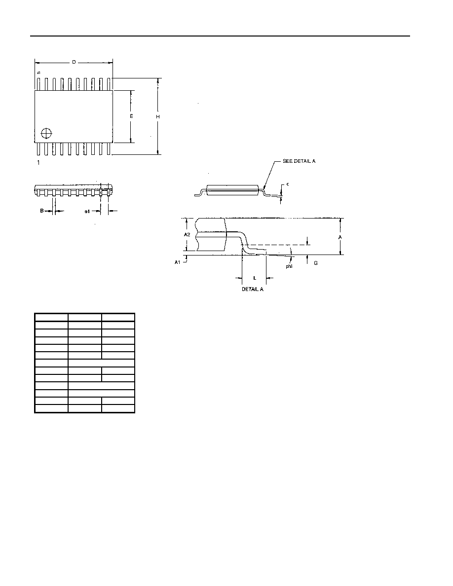
DS1306 20-PIN TSSOP
DIM
MIN
MAX
A MM
-
1.10
A1 MM
0.05
-
A2 MM
0.75
1.05
C MM
0.09
0.18
L MM
0.50
0.70
e1 MM
0.65 BSC
B MM
0.18
0.30
D MM
6.40
6.90
E MM
4.40 NOM
G MM
0.25 REF
H MM
6.25
6.55
phi
0
∞
8
∞