 | –≠–ª–µ–∫—Ç—Ä–æ–Ω–Ω—ã–π –∫–æ–º–ø–æ–Ω–µ–Ω—Ç: DS1482 | –°–∫–∞—á–∞—Ç—å:  PDF PDF  ZIP ZIP |
1 of 7
032103
DS1482
1-Wire Level Shifter and Line Driver
with Load Sensor
www.maxim-ic.com
FEATURES
ß Works with All iButtons
Æ
and 1-Wire
Æ
Devices
ß Communicates at Regular and Overdrive 1-
Wire Speed (Host-Dependent)
ß Separate Interface Power Supply to Level
Shift to Non-5V Systems
ß External Strong-Pullup Control Pin can be
Used to Provide Low-On-Resistance-High
Current Power Source
ß Load Sensor to Detect when Strong-Pullup
Power Delivery is no Longer Needed
ß Power Delivery DONE Signal can be
Connected to Host Interrupt
ß Low-Cost 16-Pin SO Surface-Mount Package
ß Operating Temperature Range: -40∞C to
+85∞C
PIN ASSIGNMENT
1
2
3
4
5
6
7
8
16
15
14
13
12
11
10
9
V
CCQ
N.C.
SPU
START
TXD
N.C.
GND
N.C.
V
CC
N.C.
PCTLZ
DONE
RXD
N.C.
I/O
N.C.
ORDERING INFORMATION
DS1482S
SO-16
DS1482S/T&R
SO-16, Tape-and-Reel
Contact the factory for versions with different
signal polarities.
DESCRIPTION
The DS1482 is a simple 1-Wire line driver with load sensor and level shifter, designed to function as an
interface between a 3V host system and a 1-Wire system that runs on 5V. Two supplies are provided, a
5V supply for the 1-Wire operations (V
CC
) and an interface supply (V
CCQ
). The DS1482 can connect
directly to a synchronous serial port if it supports the appropriate bit rates to generate 1-Wire timing.
Figure 1 shows the DS1482 block diagram. TXD is buffered and controls an N-channel transistor, which
drives the 1-Wire pin I/O low, e.g., to initiate a time slot. The logic level of the I/O pin is returned
through a level-shifting buffer to the RXD pin for the host processor to read. Figure 3 shows the
relationship of these signals in case of a 1-Wire read time slot.
The SPU input generates a control signal (PCTLZ) for an external low-impedance PMOS transistor
(Figure 2) that bypasses the 1-Wire pullup resistor (R
PUP
) to provide power for 1-Wire devices with a
high-load current. PCTLZ is gated by the inverted TXD signal. This prevents a high through-current in
case TXD and SPU are high at the same time.
The DS1482 contains a high-precision comparator because it is important for the host micro to know
when the high load on the 1-Wire side is no longer active. As shown in Figure 4, the high current load
causes a small drop of the voltage on the I/O pin. The comparator detects when the high current phase
ends, and enables DONE after the deglitching time t
CF
is over. The START signal allows the host micro
to selectively enable DONE.
iButton and 1-Wire are registered trademarks of Dallas Semiconductor.

DS1482
2 of 7
PIN
NAME
FUNCTION
1
V
CCQ
Operating voltage for all circuitry that connects to the controlling
microprocessor (TXD, RXD, START, SPU, DONE pins).
3
SPU
This line is used to control the external strong pullup function. When SPU is
low, the strong pullup (PCTLZ) is high. When SPU is high and TXD is low,
PCTLZ is low.
4
START
This line acts as an enable control for the DONE pin. If START is high, then
DONE reflects the filtered digital output of the current-sense comparator. If
START is low, then DONE is low.
5
TXD
When TXD is low, the I/O pin is pulled resistively to V
CC
. When TXD is
high, the 1-Wire bus is pulled to GND (for write-0, write-1, read, and reset
low times).
7
GND
Ground Reference for V
CCQ
, V
CC
, 1-Wire
10
I/O
1-Wire Data
12
RXD
This line returns the digital state of the 1-Wire bus, level-shifted to swing
between V
CCQ
and GND.
13
DONE
This line is high only when the buffered, filtered digital output from the
current-sense comparator indicates that the downstream 1-Wire slave device
is no longer sinking high current. This signal is enabled if START is high.
14
PCTLZ
Active-low control pin for an external low-on-resistance, high-current
supply. This signal typically controls the gate of a P-channel MOSFET. This
signal is low when SPU is high and TXD is low.
16
V
CC
Operating voltage for all circuitry that connects to the 1-Wire environment
(I/O and PCTLZ pins).
2, 6, 8, 9,
11, 15
N.C.
Not Connected
Figure 1. Block Diagram
V
CCQ
V
CC
RXD
TXD
DONE
I/O
PCTLZ
SPU
LEVEL-SHIFT BOUNDARY
START
Vref
+
-
R
PUP
GND
DS1482
3 of 7
Figure 2. Typical Operating Circuit
(21)
V
CCQ
SH7622
µC
(164)
TxD0
(171)
RxD0
(32)
PTA0
(31)
PTA1
(178)
IRQ7
V
CC
PCTLZ
V
CCQ
DS1482
TXD
I/O
RXD
SPU
START
DONE
GND
IRLMS6702
RS
V
CC
= 5V
1-Wire
NETWORK
V
CCQ
= 3.3V
Selecting RS
Assuming that the series resistance of the FET in
on-condition can be neglected, the value of RS is
limited as follows:
RSmax = 0.0015 x VCCmin/I(standby,max)
RSmin = 0.01 x VCCmax/I(active,min)
Example:
VCCmin = 4.5V, VCCmax = 5.5V
I(standby,max) = 0.15mA
I(active,min) = 12mA
RSmax = 45
W, RSmin = 4.58W
To maximize available power on the 1-Wire line,
RS should be close to the lowest permissible
value, in this example 5.1
W ±5%. The effect of the
on-chip pullup resistor is negligible.
Figure 3. DS1482 Application Signals, Normal Communication
TXD
SPU, START, DONE ALL LOW
I/O
RXD
H
L
H
L
H
L
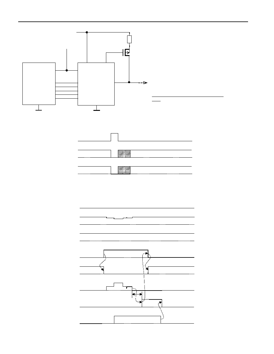
Figure 4. DS1482 Application Signals, Strong Pullup Case
TXD
SPU
RXD
I/O
START
CURRENT
t
CF
1
DONE
2
3
4
H
L
H
L
H
L
PCTLZ
H
L
H
L
H
L
H
L

DS1482
4 of 7
Point 1:
The 1-Wire slave device starts drawing current (internal micro or numeric processor is
running). The strong pullup (SPU) must be activated before the high current phase begins.
Point 2:
The 1-Wire slave device no longer draws current. After the deglitching time (t
CF
) is over, the
DONE signal turns high. The START signal must be activated no later than t
SD
before t
CF
is
over. Typically START is activated shortly after SPU, but not before the 1-Wire slave device
has started drawing high current.
Point 3:
As soon as the DONE signal is high, the host micro ends the strong pullup by changing SPU
to low.
Point 4:
While the DONE signal is high, the host micro changes START to low; this may occur
simultaneously with the state change of SPU or later. When START changes to low, DONE
becomes low.
Figure 5. Timing References TXD to I/O
TXD
I/O
0.7 x V
CCQ
0.2 x V
CCQ
0.9 x V
CC
0.1 x V
CC
t
FIO
t
TI
t
TI
Figure 6. Timing References I/O to RXD
I/O
RXD
0.7 x V
CC
0.2 x V
CC
0.9 x V
CCQ
0.1 x V
CCQ
t
F
t
R
t
IR
t
IR

DS1482
5 of 7
Figure 7. Timing References SPU to PCTLZ
SPU
PCTLZ
0.7 x V
CCQ
0.2 x V
CCQ
0.9 x V
CC
0.1 x V
CC
t
SP
t
SP
t
F
t
R
Figure 8. Timing References START to DONE
START
DONE
0.2 x V
CCQ
0.9 x V
CCQ
0.1 x V
CCQ
t
SD
t
R
t
F