 | –≠–ª–µ–∫—Ç—Ä–æ–Ω–Ω—ã–π –∫–æ–º–ø–æ–Ω–µ–Ω—Ç: DS1609 | –°–∫–∞—á–∞—Ç—å:  PDF PDF  ZIP ZIP |

DS1609
Dual Port RAM
DS1609
020499 1/7
FEATURES
∑
Totally asynchronous 256≠byte dual port memory
∑
Multiplexed address and data bus keeps pin count
low
∑
Dual port memory cell allows random access with
minimum arbitration
∑
Each port has standard independent RAM control sig-
nals
∑
Fast access time
∑
Low power CMOS design
∑
24≠pin DIP or 24≠pin SOIC surface mount package
∑
Both CMOS and TTL compatible
∑
Operating temperature of ≠40
∞
C to +85
∞
C
∑
Standby current of 100 nA @ 25
∞
C makes the device
ideal for battery backup or battery operate applica-
tions.
PIN ASSIGNMENT
DS1609S
24≠PIN SOIC (300 MIL)
V
CC
OE
B
CE
B
WE
B
AD0
B
AD1
B
AD2
B
AD3
B
AD4
B
AD5
B
AD6
B
AD7
B
AD7
A
AD6
A
AD5
A
AD4
A
AD3
A
AD2
A
AD1
A
AD0
A
WE
A
CE
A
OE
A
GND
PORT A
DS1609
24≠PIN DIP (600 MIL)
PORT A
PORT B
V
CC
OE
B
CE
B
WE
B
AD0
B
AD1
B
AD2
B
AD3
B
AD4
B
AD5
B
AD6
B
AD7
B
AD7
A
AD6
A
AD5
A
AD4
A
AD3
A
AD2
A
AD1
A
AD0
A
WE
A
CE
A
OE
A
GND
1
2
3
4
5
6
7
8
9
10
11
12
24
23
22
21
20
19
18
17
16
15
14
13
1
2
3
4
5
6
7
8
9
10
11
12
24
23
22
21
20
19
18
17
16
15
14
13
See Mech. Drawings
Section
See Mech. Drawings
Section
PORT B
PIN DESCRIPTION
AD0≠AD7
≠ Port address/data
CE
≠ Port enable
WE
≠ Write enable
OE
≠ Output enable
V
CC
≠ +5 volt supply
GND
≠ Ground
DESCRIPTION
The DS1609 is a random access 256≠byte dual port
memory designed to connect two asyncronous ad-
dress/data buses together with a common memory ele-
ment. Both ports have unrestricted access to all
256 bytes of memory, and with modest system disci-
pline no arbitration is required. Each port is controlled
by three control signals: output enable, write enable,
and port enable. The device is packaged in plastic
24≠pin DIP and 24≠pin SOIC. Output enable access
time of 50 ns is available when operating at 5 volts.

DS1609
020499 2/7
OPERATION ≠ READ CYCLE
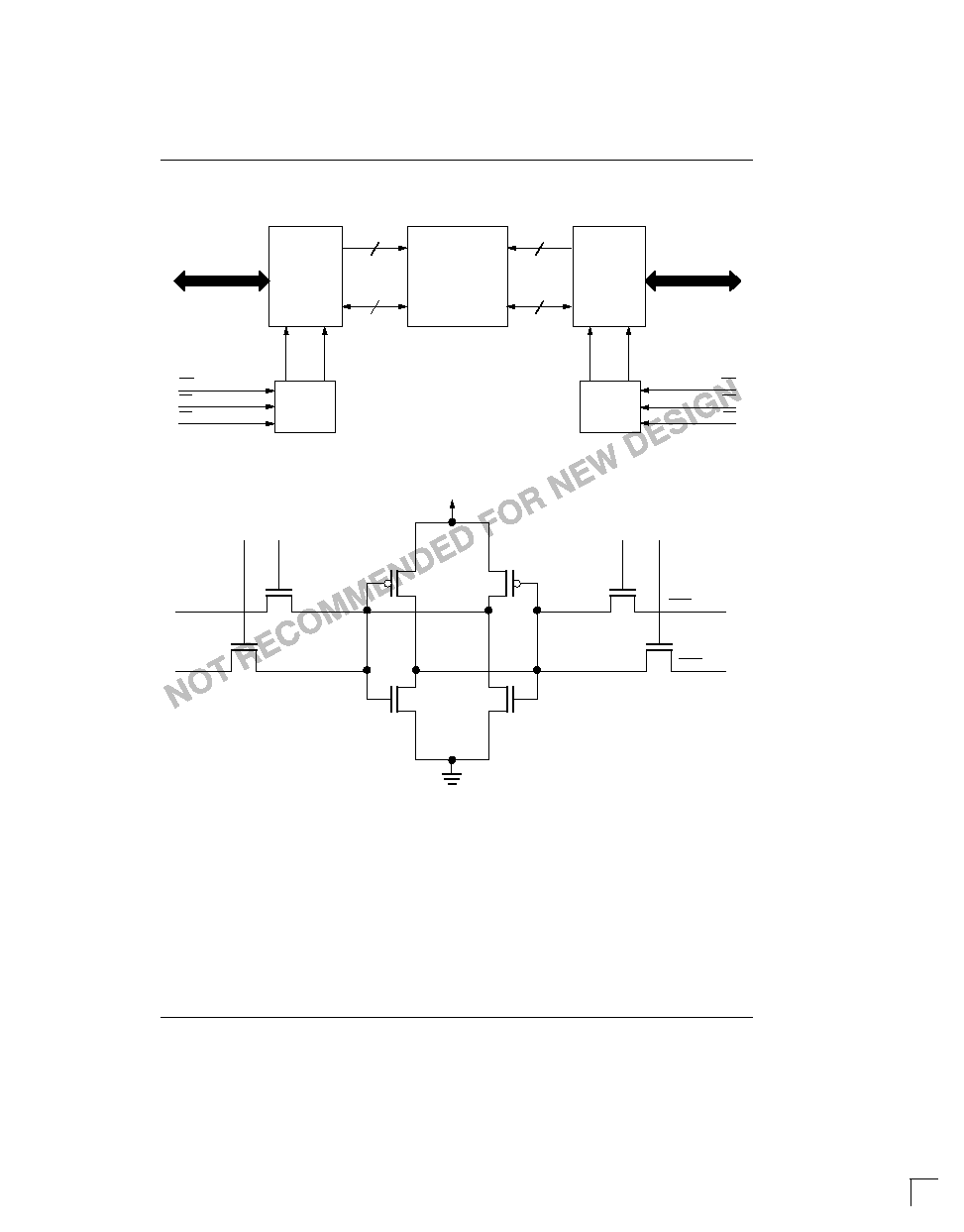
The main elements of the dual port RAM are shown in
Figure 1.
A read cycle to either port begins by placing an address
on the multiplexed bus pins AD0 ≠ AD7. The port enable
control (CE) is then transitioned low. This control signal
causes address to be latched internally. Addresses can
be removed from the bus provided address hold time is
met. Next, the output enable control (OE) is transitioned
low, which begins the data access portion of the read
cycle. With both CE and OE active low, data will appear
valid after the output enable access time t
OEA
. Data will
remain valid as long as both port enable and output en-
able remains low. A read cycle is terminated with the
first occurring rising edge of either CE or OE. The ad-
dress/data bus will return to a high impedance state af-
ter time t
CEZ
or t
OEZ
as referenced to the first occurring
rising edge. WE must remain high during read cycles.
OPERATION ≠ WRITE CYCLE
A write cycle to either port begins by placing an address
on the multiplexed bus pins AD0 ≠ AD7. The port enable
control (CE) is then transitioned low. This control signal
causes address to be latched internally. As with a read
cycle, the address can be removed from the bus pro-
vided address hold time is met. Next the write enable
control signal (WE) is transitioned low which begins the
write data portion of the write cycle. With both CE and
WE active low the data to be written to the selected
memory location is placed on the multiplexed bus. Pro-
vided that data setup (t
DS
) and data hold (t
DH
) times are
met, data is written into the memory and the write cycle
is terminated on the first occurring rising edge of either
CE or WE. Data can be removed from the bus as soon
as the write cycle is terminated. OE must remain high
during write cycles.
ARBITRATION
The DS1609 dual port RAM has a special cell design
that allows for simultaneous accesses from two ports
(see Figure 2). Because of this cell design, no arbitra-
tion is required for read cycles occurring at the same in-
stant. However, an argument for arbitration can be
made for reading and writing the cell at the exact same
instant or for writing from both ports at the same instant.
A simple way to assure that read/write conflicts don't oc-
cur is to perform redundant read cycles. Write/write ar-
bitration needs can be avoided by assigning groups of
addresses for write operation to one port only. Groups
of data can be assigned check sum bytes which would
guarantee correct transmission. A software arbitration
system using a "mail box" to pass status information can
also be employed. Each port could be assigned a
unique byte for writing status information which the oth-
er port would read. The status information could tell the
reading port if any activity is in progress and indicate
when activity is going to occur.

DS1609
020499 3/7
BLOCK DIAGRAM: DUAL PORT RAM Figure 1
PORT A
MUX ADDRESS/DATA
ADDRESS/
DATA MUX
LATCH
DECODE
256 BYTE DUAL
PORT MEMORY
MATRIX
8 ADDRESS
8 DATA
8 ADDRESS
8 DATA
PORT B
ADDRESS/
DATA MUX
LATCH
DECODE
MUX ADDRESS/DATA
WE
OE
CE
CONTROL
LOGIC
CONTROL
LOGIC
WE
OE
CE
DUAL PORT MEMORY CELL Figure 2
V
CC
DATA≠PORT A
DATA≠PORT B
DATA≠PORT A
DATA≠PORT B

DS1609
020499 4/7
ABSOLUTE MAXIMUM RATINGS*
Voltage on Any Pin Relative to Ground
≠0.5V to +7.0V
Operating Temperature
≠40
∞
C to +85
∞
C
Storage Temperature
≠55
∞
C to +125
∞
C
Soldering Temperature
260
∞
C for 10 seconds
* This is a stress rating only and functional operation of the device at these or any other conditions above those
indicated in the operation sections of this specification is not implied. Exposure to absolute maximum rating
conditions for extended periods of time may affect reliability.
RECOMMENDED DC OPERATING CONDITIONS
(≠40
∞
C to +85
∞
C)
PARAMETER
SYMBOL
MIN
TYP
MAX
UNITS
NOTES
Power Supply
V
CC
4.5
5.0
5.5
V
1
Input Logic 1
V
IH
2.0
V
CC
+ 0.3
V
1
Input Logic 0
V
IL
≠0.3
+0.8
V
1
DC ELECTRICAL CHARACTERISTICS
(≠40
∞
C to +85
∞
C; V
CC
= 5V
±
10%)
PARAMETER
SYMBOL
MIN
TYP
MAX
UNITS
NOTES
Input Impedance
Z
IN
50K
2
CE, WE, OE Leakage
I
LO
≠1.0
+1.0
µ
A
Standby Current
I
CCS1
3.0
5.0
mA
3, 4, 13
Standby Current
I
CCS2
50
300
µ
A
3, 5, 13
Standby Current
I
CCS3
100
nA
3, 6, 13
Operating Current
I
CC
18
30
mA
7, 13
Logic 1 Output
V
OH
2.4
V
8
Logic 0 Output
V
OL
0.4
V
9
CAPACITANCE
(t
A
= 25
∞
C)
PARAMETER
SYMBOL
MIN
TYP
MAX
UNITS
NOTES
Input Capacitance
C
IN
5
10
pF
I/O Capacitance
C
I/O
5
10
pF

DS1609
020499 5/7
AC ELECTRICAL CHARACTERISTICS
(≠40
∞
C to +85
∞
C; V
CC
= 5V
±
10%)
PARAMETER
SYMBOL
MIN
TYP
MAX
UNITS
NOTES
Address Setup Time
t
AS
5
ns
Address Hold Time
t
AH
25
ns
Output Enable Access
t
OEA
0
50
ns
10
OE to High Z
t
OEZ
0
20
ns
CE to High Z
t
CEZ
0
20
ns
Data Setup Time
t
DS
0
ns
Data Hold Time
t
DH
10
ns
Write Pulse Width
t
WP
50
ns
11
CE Recovery Time
t
CER
20
ns
12
WE Recovery Time
t
WER
20
ns
12
OE Recovery Time
t
OER
20
ns
12
CE to OE Setup Time
t
COE
25
ns
CE to WE Setup Time
t
CWE
25
ns
AC ELECTRICAL CHARACTERISTICS
(≠40
∞
C to +85
∞
C; V
CC
= 2.5V ≠ 4.5V)
PARAMETER
SYMBOL
MIN
TYP
MAX
UNITS
NOTES
Address Setup Time
t
AS
5
ns
Address Hold Time
t
AH
25
ns
Output Enable Access
t
OEA
0
100
ns
10
OE to High Z
t
OEZ
0
20
ns
CE to High Z
t
CEZ
0
20
ns
Data Setup Time
t
DS
0
ns
Data Hold Time
t
DH
10
ns
Write Pulse Width
t
WP
100
ns
11
CE Recovery Time
t
CER
20
ns
12
WE Recovery Time
t
WER
20
ns
12
OE Recovery Time
t
OER
20
ns
12
CE to OE Setup Time
t
COE
25
ns
CE to WE Setup Time
t
CWE
25
ns

DS1609
020499 6/7
DUAL PORT RAM TIMING: READ CYCLE
AD0 ≠ AD7
DURING READ CYCLE WE = V
IH
ADDRESS VALID
DON'T CARE
DATA OUT VALID
t
AS
t
AH
t
COE
t
OEA
t
OEZ
t
CEZ
CE
OE
NOTES:
1. During read cycle the address must be off the bus prior to t
OEA
minimum to avoid bus contention.
2. Read cycles are terminated by the first occurring rising edge of OE or CE.
DUAL PORT RAM TIMING: WRITE CYCLE
AD0 ≠ AD7
DURING WRITE CYCLE OE = V
IH
ADDRESS VALID
DON'T CARE
DATA IN VALID
t
AS
t
AH
t
CWE
t
DH
CE
WE
t
DS
t
WP
NOTE:
1. Write cycles are terminated by the first occurring edge of WE or CE.

DS1609
020499 7/7
NOTES:
1. All Voltages are referenced to ground.
2. All pins other than CE, WE, OE, V
CC
and ground are continuously driven by a feedback latch in order to hold the
inputs at one power supply rail or the other when an input is tristated. The minimum driving impedance presented
to any pin is 50K
. If a pin is at a logic low level, this impedance will be pulling the pin to ground. If a pin is at a
logic high level, this impedance will be pulling the pin to V
CC
.
3. Standby current is measured with outputs open circuited.
4. I
CCS1
is measured with all pins within 0.3V of V
CC
or GND and with CE at a logic high or logic low level.
5. I
CCS2
is measured with all pins within 0.3V of V
CC
or ground and with CE within 0.3V of V
CC
.
6. I
CCS3
is measured with all pins at V
CC
or ground potential and with CE = V
CC
. Note that if a pin is floating, the
internal feedback latches will pull all the pins to one power supply rail or the other.
7. Active current is measured with outputs open circuited, and inputs swinging full supply levels with one port reading
and one port writing at 100 ns cycle time. Active currents are a DC average with respect to the number of 0's and
1's being read or written.
8. Logic one voltages are specified at a source current of 1 mA.
9. Logic zero voltages are specified at a sink current of 4 mA.
10. Measured with a load as shown in Figure 3.
11. t
WP
is defined as the time from WE going low to the first of the rising edges of WE and CE.
12. Recovery time is the amount of time control signals must remain high between successive cycles.
13. Typical values are at 25
∞
C.
LOAD SCHEMATIC Figure 3
+5 VOLTS
30 pF
D.U.T.
1.1K
680


