 | –≠–ª–µ–∫—Ç—Ä–æ–Ω–Ω—ã–π –∫–æ–º–ø–æ–Ω–µ–Ω—Ç: DS1644 | –°–∫–∞—á–∞—Ç—å:  PDF PDF  ZIP ZIP |
E
Copyright 1995 by Dallas Semiconductor Corporation.
All Rights Reserved. For important information regarding
patents and other intellectual property rights, please refer to
Dallas Semiconductor data books.
DS1644LPM
Nonvolatile Timekeeping RAM
DS1644LPM
041697 1/11
FEATURES
∑
Upward compatible with the DS1643AL Timekeeping
RAM to achieve higher RAM density
∑
Integrated NV SRAM, real time clock, crystal, power≠
fail control circuit and lithium energy source
∑
Low profile socketable module
≠ 255 mil package height
∑
Clock registers are accessed identical to the static
RAM. These registers are resident in the eight top
RAM locations.
∑
Totally nonvolatile with over 10 years of operation in
the absence of power
∑
Access time of 120 ns and 150 ns
∑
Quartz accuracy
±
1 minute a month @ 25
∞
C, factory
calibrated
∑
BCD coded year, month, date, day, hours, minutes,
and seconds with leap year compensation valid up to
2100
∑
Power≠fail write protection allows for
±
10% V
CC
pow-
er supply tolerance
ORDERING INFORMATION
DS1644L≠XXX
≠120
120 ns access
150 ns access
≠150
Low Profile Module
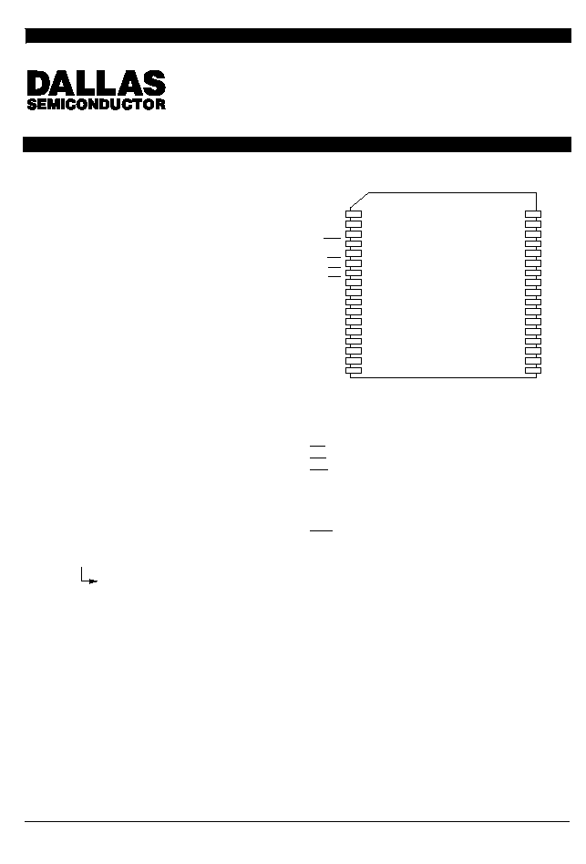
PIN ASSIGNMENT
OE
CE
WE
PFO
V
CC
1
2
3
4
5
6
7
8
9
10
11
12
13
34
33
32
31
30
29
28
27
26
25
24
23
22
14
15
16
17
21
20
19
18
NC
NC
A14
A13
A12
A11
A10
A9
A8
A7
A6
A5
A4
A3
A2
A1
A0
NC
NC
NC
DQ7
DQ6
DQ5
DQ4
DQ3
DQ2
DQ1
DQ0
GND
34≠PIN LOW PROFILE MODULE
PIN DESCRIPTION
A0≠A14
≠ Address Input
CE
≠ Chip Enable
OE
≠ Output Enable
WE
≠ Write Enable
V
CC
≠ +5 Volts
GND
≠ Ground
DQ0-DQ7
≠ Data Input/Output
NC
≠ No Connection
PFO
≠ Power Fail Output
DESCRIPTION
The DS1644L is a low profile module that requires a
PLCC surface mountable socket and is functionally
equivalent to the DS1644. The DS1644L is a 32K x 8
nonvolatile static RAM with a full function real time clock
which are both accessible in a Byte≠wide format. The
real time clock information resides in the eight upper-
most RAM locations. The RTC registers contain year,
month, date, day, hours, minutes, and seconds data in
24 hour BCD format. Corrections for the day of the
month and leap year are made automatically. The RTC
clock registers are double buffered to avoid access of in-
correct data that can occur during clock update cycles.
The double buffered system also prevents time loss as
the timekeeping countdown continues unabated by ac-
cess to time register data. The DS1644L also contains
its own power≠fail circuitry which deselects the device
when the V
CC
supply is in an out≠of≠tolerance condi-
tion. This feature prevents loss of data from unpredict-
able system operation brought on by low V
CC
as errant
access and update cycles are avoided.

DS1644LPM
041697 2/11
CLOCK OPERATIONS ≠
READING THE CLOCK
While the double buffered register structure reduces the
chance of reading incorrect data, internal updates to the
DS1644L clock registers should be halted before clock
data is read to prevent reading of data in transition.
However, halting the internal clock register updating
process does not affect clock accuracy. Updating is
halted when a one is written into the read bit, the seventh
most significant bit in the control register. As long as a
one remains in that position, updating is halted. After a
halt is issued, the registers reflect the count, that is day,
date, and time that was current at the moment the halt
command was issued. However, the internal clock reg-
isters of the double buffered system continue to update
so that the clock accuracy is not affected by the access
of data. All of the DS1644L registers are updated simul-
taneously after the clock status is reset. Updating is
within a second after the read bit is written to zero.
DS1644L BLOCK DIAGRAM Figure 1
OSCILLATOR AND
CLOCK COUNTDOWN
CHAIN
POWER MONITOR,
SWITCHING, AND
WRITE PROTECTION
V
CC
POWER GOOD
CLOCK
REGISTERS
CE
WE
A0≠A14
DQ0≠DQ7
32.768 KHz
+
OE
32K X 8
NV SRAM
PFO
V
BAT

DS1644LPM
041697 3/11
DS1644L TRUTH TABLE Table 1
V
CC
CE
OE
WE
MODE
DQ
POWER
5 VOLTS
10%
V
IH
X
X
DESELECT
HIGH≠Z
STANDBY
5 VOLTS
10%
X
X
X
DESELECT
HIGH≠Z
STANDBY
5 VOLTS
±
10%
V
IL
X
V
IL
WRITE
DATA IN
ACTIVE
V
IL
V
IL
V
IH
READ
DATA OUT
ACTIVE
V
IL
V
IH
V
IH
READ
HIGH≠Z
ACTIVE
<4.5 VOLTS
>V
BAT
X
X
X
DESELECT
HIGH≠Z
CMOS STANDBY
<V
BAT
X
X
X
DESELECT
HIGH≠Z
DATA RETENTION
MODE
SETTING THE CLOCK
The eighth bit of the control register is the write bit. Set-
ting the write bit to a one, like the read bit, halts updates
to the DS1644L registers. The user can then load them
with the correct day, date and time data in 24 hour BCD
format. Resetting the write bit to a zero then transfers
those values to the actual clock counters and allows
normal operation to resume.
STOPPING AND STARTING THE CLOCK
OSCILLATOR
The clock oscillator may be stopped at any time. To in-
crease the shelf life, the oscillator can be turned off to
minimize current drain from the battery. The OSC bit is
the MSB for the seconds registers. Setting it to a one
stops the oscillator.
FREQUENCY TEST BIT
Bit 6 of the day byte is the frequency test bit. When the
frequency test bit is set to logic "1" and the oscillator is
running, the LSB of the seconds register will toggle at
512 Hz. When the seconds register is being read, the
DQ0 line will toggle at the 512 Hz frequency as long as
conditions for access remain valid (i.e., CE low, OE low,
and address for seconds register remain valid and
stable).
CLOCK ACCURACY
The DS1644L is guaranteed to keep time accuracy to
within
±
1 minute per month at 25
∞
C. The clock is cali-
brated at the factory by Dallas Semiconductor using
special calibration nonvolatile tuning elements. The
DS1644L does not require additional calibration, and
temperature deviations will have a negligible effect in
most applications. For this reason, methods of field
clock calibration are not available and not necessary.
Attempts to calibrate the clock that may be used with
similar device types (MK48T08 family) will not have any
effect even though the DS1644L appears to accept cal-
ibration data.

DS1644LPM
041697 4/11
DS1644L REGISTER MAP ≠ BANK1 Table 2
ADDRESS
DATA
FUNCTION
ADDRESS
B
7
B
6
B
5
B
4
B
3
B
2
B
1
B
0
FUNCTION
7FFF
≠
≠
≠
≠
≠
≠
≠
≠
YEAR
00≠99
7FFE
X
X
X
≠
≠
≠
≠
≠
MONTH
01≠12
7FFD
X
X
≠
≠
≠
≠
≠
≠
DATE
01≠31
7FFC
X
FT
X
X
X
≠
≠
≠
DAY
01≠07
7FFB
X
X
≠
≠
≠
≠
≠
≠
HOUR
00≠23
7FFA
X
≠
≠
≠
≠
≠
≠
≠
MINUTES
00≠59
7FF9
OSC
≠
≠
≠
≠
≠
≠
≠
SECONDS
00≠59
7FF8
W
R
X
X
X
X
X
X
CONTROL
A
OSC = STOP BIT
R
=
READ BIT
FT =
FREQUENCY TEST
W
= WRITE BIT
X
=
UNUSED
NOTE:
All indicated "X" bits are not dedicated to any particular function and can be used as normal RAM bits.
RETRIEVING DATA FROM RAM OR CLOCK
The DS1644L is in the read mode whenever WE (write
enable) is high, and CE (chip enable) is low. The device
architecture allows ripple-through access to any of the
address locations in the NV SRAM. Valid data will be
available at the DQ pins within t
AA
after the last address
input is stable, providing that the CE and OE access
times and states are satisfied. If CE or OE access times
are not met, valid data will be available at the latter of
chip enable access (t
CEA
) or at output enable access
time (t
OEA
). The state of the data input/output pins (DQ)
is controlled by CE and OE. If the outputs are activated
before t
AA
, the data lines are driven to an intermediate
state until t
AA
. If the address inputs are changed while
CE and OE remain valid, output data will remain valid for
output data hold time (t
OH
) but will then go indeterminate
until the next address access.
WRITING DATA TO RAM OR CLOCK
The DS1644L is in the write mode whenever WE and
CE are in their active state. The start of a write is refer-
enced to the latter occurring high to low transition of WE
or CE. The addresses must be held valid throughout the
cycle. CE or WE must return inactive for a minimum of
t
WR
prior to the initiation of another read or write cycle.
Data in must be valid t
DS
prior to the end of write and re-
main valid for t
DH
afterward. In a typical application, the
OE signal will be high during a write cycle. However,
OE can be active provided that care is taken with the
data bus to avoid bus contention. If OE is low prior to
WE transitioning low the data bus can become active
with read data defined by the address inputs. A low tran-
sition on WE will then disable the outputs t
WEZ
after WE
goes active.

DS1644LPM
041697 5/11
DATA RETENTION MODE
When V
CC
is within nominal limits (V
CC
> 4.5 volts) the
DS1644L can be accessed as described above with
read or write cycles. However, when V
CC
is below the
power fail point V
PF
(point at which write protection oc-
curs) the internal clock registers and RAM are blocked
from access. This is accomplished internally by inhibit-
ing access via the CE signal. At this time the power≠fail
output signal (PFO) will be driven active low and will
remain active until V
CC
returns to nominal levels. When
V
CC
falls below the level of the internal battery supply,
power input is switched from the V
CC
pin to the internal
battery and clock activity, RAM, and clock data are
maintained from the battery until V
CC
is returned to
nominal level.
INTERNAL BATTERY LONGEVITY
The DS1644L has a self contained lithium power source
that is designed to provide energy for clock activity, and
clock and RAM data retention when the V
CC
supply is
not present. The capability of this internal power supply
is sufficient to power the DS1644L continuously for the
life of the equipment in which it is installed. For specifi-
cation purposes, the life expectancy is 10 years at 25
∞
C
with the internal clock oscillator running in the absence
of V
CC
power. The DS1644L is shipped from Dallas
Semiconductor with the clock oscillator turned off, so
the expected life should be considered to start from the
time the clock oscillator is first turned on. Actual life ex-
pectancy of the DS1644L will be much longer than 10
years since no internal lithium battery energy is con-
sumed when V
CC
is present. In fact, in most applica-
tions, the life expectancy of the DS1644L will be approx-
imately equal to the shelf life (expected useful life of the
lithium battery with no load attached) of the lithium bat-
tery which may prove to be as long as 20 years.