 | –≠–Ľ–Ķ–ļ—ā—Ä–ĺ–Ĺ–Ĺ—č–Ļ –ļ–ĺ–ľ–Ņ–ĺ–Ĺ–Ķ–Ĺ—ā: DS1707 | –°–ļ–į—á–į—ā—Ć:  PDF PDF  ZIP ZIP |
E
Copyright 1995 by Dallas Semiconductor Corporation.
All Rights Reserved. For important information regarding
patents and other intellectual property rights, please refer to
Dallas Semiconductor data books.
DS1707/DS1708
3.3 and 5.0 Volt MicroMonitor
DS1707/DS1708
010996 1/9
FEATURES
∑
Holds microprocessor in check during power tran-
sients
∑
Automatically restarts microprocessor after power
failure
∑
Monitors pushbutton for external override
∑
Accurate 5%, 10% or 20% resets for 3.3 systems and
5% or 10% resets for 5.0 volt systems
∑
Eliminates the need for discrete components
∑
20% tolerance compatible with 3.0 volt systems
∑
Pin compatible with the MAXIM MAX707/MAX708 in
8≠pin DIP and 8≠pin SOIC packages
∑
8≠pin DIP, 8≠pin SOIC and 8≠pin
Ķ
≠SOP packages
available
∑
Industrial temperature range ≠40
į
C to +85
į
C
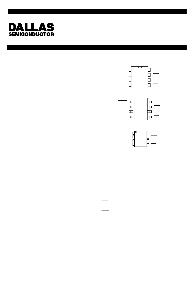
PIN ASSIGNMENT
RST
RST
NC
NMI
1
2
3
4
PBRST
V
CC
GND
IN
8
7
6
5
8
7
6
5
1
2
3
4
PBRST
V
CC
GND
IN
RST
RST
NC
NMI
8≠PIN DIP
(300 MIL)
8≠PIN SOIC
(150 MIL)
1
2
3
4
8
7
6
5
PBRST
V
CC
GND
IN
RST
RST
NC
NMI
8≠PIN
Ķ
≠SOP
(118 MIL)
See Mech. Drawings
Section
DS1707 and DS1708_/R/S/T
PIN DESCRIPTION
PBRST
≠ Pushbutton Reset Input
V
CC
≠ Power Supply
GND
≠ Ground
IN
≠ Input
NMI
≠ Non≠maskable Interrupt
NC
≠ No Connect
RST
≠ Active Low Reset Output
RST
≠ Active High Reset Output
DESCRIPTION
The DS1707/DS1708 3.3 or 5.0 Volt MicroMonitor moni-
tors three vital conditions for a microprocessor: power
supply, voltage sense, and external override. A preci-
sion temperature≠compensated reference and
comparator circuit monitors the status of V
CC
at the
device and at an upstream point for maximum protec-
tion. When the sense input detects an out≠of≠tolerance
condition a non≠maskable interrupt is generated. As
the voltage at the device degrades an internal power fail
signal is generated which forces the reset to an active
state. When V
CC
returns to an in≠tolerance condition,
the reset signal is kept in the active state for a minimum
of 130 ms to allow the power supply and processor to
stabilize.

DS1707/DS1708
010996 2/9
The third function the DS1707/DS1708 performs is
pushbutton reset control. The DS1707/DS1708
debounces the pushbutton input and guarantees an
active reset pulse width of 130 ms minimum.
OPERATION
Power Monitor
The DS1707/DS1708 detects out≠of≠tolerance power
supply conditions and warns a processor≠based sys-
tem of impending power failure. When V
CC
falls below
the minimum V
CC
tolerance, a comparator outputs the
RST and RST signals. RST and RST are excellent con-
trol signals for a microprocessor, as processing is
stopped at the last possible moment of valid V
CC
. On
power≠up, RST and RST are kept active for a minimum
of 130 ms to allow the power supply and processor to
stabilize.
Pushbutton Reset
The DS1707/DS1708 provides an input pin for direct
connection to a pushbutton reset (see Figure 2). The
pushbutton reset input requires an active low signal.
Internally, this input is debounced and timed such that
RST and RST signals of at least 130 ms minimum will be
generated. The 130 ms delay commences as the push-
button reset input is released from the low level. The
pushbutton can be initiated by connecting the NMI out-
put to the PBRST input as shown in Figure 3.
Non≠Maskable Interrupt
The DS1707/DS1708 generates a non≠maskable inter-
rupt (NMI) for early warning of a power failure. A preci-
sion comparator monitors the voltage level at the IN pin
relative to an on≠chip reference generated by an inter-
nal band gap. The IN pin is a high impedance input
allowing for a user≠defined sense point. An external
resistor voltage divider network (Figure 5) is used to
interface with high voltage signals. This sense point
may be derived from a regulated supply or from a higher
DC voltage level closer to the main system power input.
Since the IN trip point V
TP
is 1.25 volts, the proper val-
ues for R1 and R2 can be determined by the equation as
shown in Figure 5. Proper operation of the
DS1707/DS1708 requires that the voltage at the IN pin
be limited to V
CC
. Therefore, the maximum allowable
voltage at the supply being monitored (V
MAX
) can also
be derived as shown in Figure 5. A simple approach to
solving the equation is to select a value for R2 high
enough to keep power consumption low, and solve for
R1. The flexibility of the IN input pin allows for detection
of power loss at the earliest point in a power supply sys-
tem, maximizing the amount of time for system shut≠
down between NMI and RST/RST.
When the supply being monitored decays to the voltage
sense point, the DS1707/DS1708 pulses the NMI out-
put to the active state for a minimum 200
Ķ
s. The NMI
power fail detection circuitry also has built≠in hysteresis
of 100
Ķ
V. The supply must be below the voltage sense
point for approximately 5
Ķ
s before a low NMI will be
generated. In this way, power supply noise is removed
from the monitoring function, preventing false inter-
rupts. During a power≠up, any detected IN pin levels
below V
TP
by the comparator are disabled from gener-
ating an interrupt until V
CC
rises to V
CCTP
. As a result,
any potential NMI pulse will not be initiated until V
CC
reaches V
CCTP
.
Connecting NMI to PBRST would allow the non≠mask-
able interrupt to generate an automatic reset when an
out≠of≠tolerance condition occurred in a monitored
supply. An example is shown in Figure 3.
DS1707/DS1708
010996 3/9
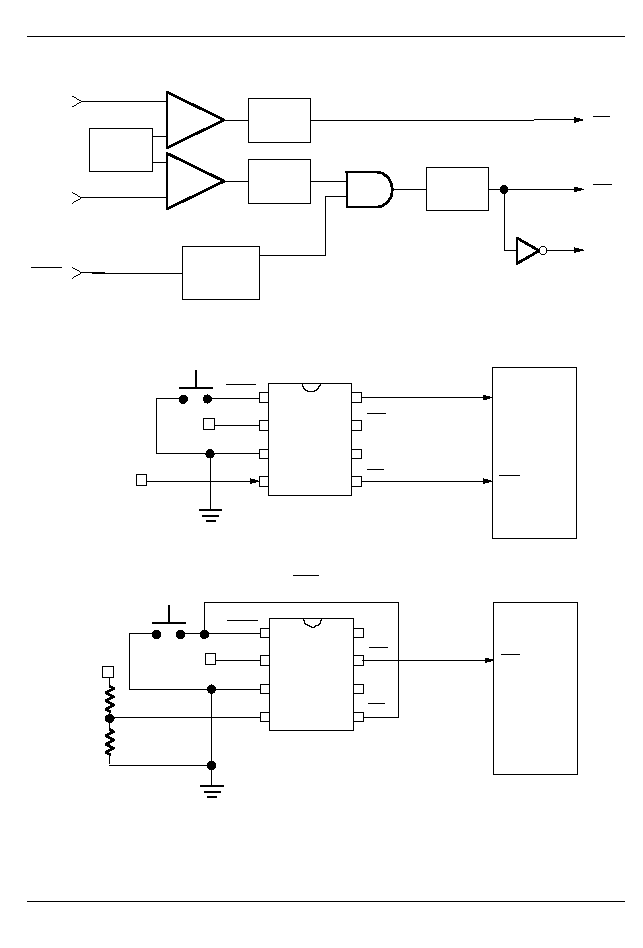
MICROMONITOR BLOCK DIAGRAM
Figure 1
≠
+
≠
+
T.C.
REFERENCE
DIGITAL
SAMPLER
DIGITAL
SAMPLER
DIGITAL
DELAY
LEVEL SENSE
AND
DEBOUNCE
IN
V
CC
PBRST
NMI
RST
RST
PUSHBUTTON RESET Figure 2
GND
IN
RST
NC
RST
PBRST
V
CC
DS1708
RST
NMI
8051
Ķ
P
5V
UPSTREAM
SUPPLY
VOLTAGE
INT0
PUSHBUTTON RESET CONTROLLED BY NMI Figure 3
GND
IN
NC
RST
PBRST
V
CC
DS1707
RST
NMI
Ķ
P
RST
UPSTREAM
SUPPLY
VOLTAGE
5V

DS1707/DS1708
010996 4/9
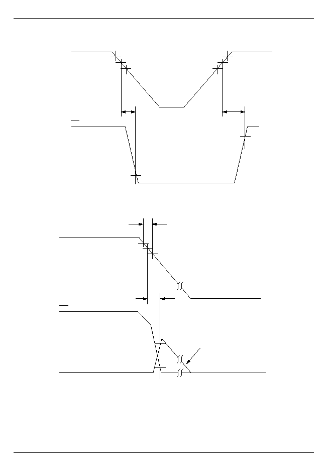
TIMING DIAGRAM: PUSHBUTTON RESET Figure 4
RST
PBRST
RST
V
IH
t
RST
V
IL
t
PDLY
t
PB
V
OH
V
OL
NON≠MASKABLE INTERRUPT CIRCUIT EXAMPLE Figure 5
GND
IN
NC
RST
PBRST
V
CC
DS1708
RST
NMI
TO
Ķ
P
R1
R2
V
SENSE
V
SENSE
+
R1
)
R2
R2
x 1.25
V
MAX
+
V
SENSE
V
TP
x V
CC
Example:
V
SENSE
= 4.70 volts at the trip point
V
CC
= 3.3 volts
10K
= R2
Therefore:
4.70
1.25
x 3.3
+
12.4 volts maximum
4.5
+
R1
)
10K
10K
x 1.25
R1
+
27.6K
W
DS1707/DS1708
010996 5/9
TIMING DIAGRAM: NON≠MASKABLE INTERRUPT Figure 6
V
IN
> 1.25V
NMI
V
OL
V
OH
V
TP(MAX)
V
TP(MAX)
V
TP
V
TP
V
TP(MIN)
V
TP(MIN)
t
IPD
t
IPD
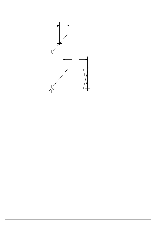
TIMING DIAGRAM: POWER DOWN Figure 7
RST SLEWS WITH V
CC
V
OL
V
OH
V
CCTP(MIN)
V
CCTP(MAX)
V
CCTP
t
RPD
t
F
V
CC
RST
RST
DS1707/DS1708
010996 6/9
TIMING DIAGRAM: POWER UP Figure 8
RST
RST
RST
RST
V
OH
V
OL
t
RPU
V
CCTP(MAX)
V
CCTP
V
CCTP(MIN)
V
CC
t
R

DS1707/DS1708
010996 7/9
ABSOLUTE MAXIMUM RATINGS*
Voltage on V
CC
Pin Relative to Ground
≠0.5V to +7.0V
Voltage on I/O Relative to Ground
≠0.5V to V
CC
+0.5V
Operating Temperature
≠40
į
C to +85
į
C
Storage Temperature
≠55
į
C to +125
į
C
Soldering Temperature
260
į
C for 10 seconds
* This is a stress rating only and functional operation of the device at these or any other conditions above those
indicated in the operation sections of this specification is not implied. Exposure to absolute maximum rating
conditions for extended periods of time may affect reliability.
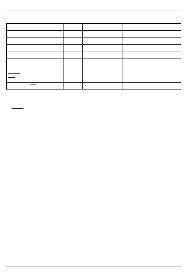
RECOMMENDED DC OPERATING CONDITIONS
(≠40
į
C to +85
į
C)
PARAMETER
SYMBOL
MIN
TYP
MAX
UNITS
NOTES
Supply Voltage
V
CC
1.0
5.5
V
1
PBRST Input High Level
V
IH
2.0
V
CC
≠0.5
V
CC
+0.3
V
1, 3
1, 4
PBRST Input Low Level
V
IL
≠0.03
+0.5
V
1
DC ELECTRICAL CHARACTERISTICS
(≠40
į
C to +85
į
C; V
CC
=1.2V to 5.5V)
PARAMETER
SYMBOL
MIN
TYP
MAX
UNITS
NOTES
V
CC
Trip Point DS1707
V
CCTP
4.50
4.65
4.75
V
1
V
CC
Trip Point DS1708
V
CCTP
4.25
4.40
4.50
V
1
V
CC
Trip Point DS1708T
V
CCTP
3.00
3.08
3.15
V
1
V
CC
Trip Point DS1708S
V
CCTP
2.85
2.93
3.00
V
1
V
CC
Trip Point DS1708R
V
CCTP
2.55
2.63
2.70
V
1
Input Leakage
I
IL
≠1.0
+1.0
Ķ
A
2
Output Current @ 2.4 volts
I
OH
350
Ķ
A
3
Output Current @ 0.4 volts
I
OL
10
mA
3
Output Voltage
V
OH
V
CC
≠0.1
V
3
Operating Current
@ V
CC
< 5.5 volts
I
CC
60
Ķ
A
5
Operating Current
@ V
CC
< 3.6 volts
I
CC
50
Ķ
A
5
IN Input Trip Point
V
TP
1.20
1.25
1.30
V
1
CAPACITANCE
(t
A
=25
į
C)
PARAMETER
SYMBOL
MIN
TYP
MAX
UNITS
NOTES
Input Capacitance
C
IN
5
pF
Output Capacitance
C
OUT
7
pF
DS1707/DS1708
010996 8/9
AC ELECTRICAL CHARACTERISTICS
(≠40
į
C to +85
į
C; V
CC
=1.2V to 5.5V)
PARAMETER
SYMBOL
MIN
TYP
MAX
UNITS
NOTES
PBRST = V
IL
t
PB
150
ns
Reset Active Time
t
RST
130
205
285
ms
V
CC
Detect to RST and RST
t
RPD
5
8
Ķ
s
7
V
CC
Slew Rate
t
F
20
Ķ
s
V
CC
Detect to RST and RST
t
RPU
130
205
285
ms
6
V
CC
Slew Rate
t
R
0
ns
PBRST Stable Low to RST and
RST
t
PDLY
250
ns
VIN Detect to NMI
t
IPD
5
8
Ķ
s
7
NOTES:
1. All voltages are referenced to ground.
2. PBRST is internally pulled up to V
CC
with an internal impedance of 40K
typical.
3. V
CC
2.4 volts
4. V
CC
< 2.4 volts
5. Measured with outputs open and all inputs at V
CC
or ground.
6. t
R
= 5
Ķ
s
7. Noise immunity ≠ pulses < 2
Ķ
s at V
CCTP
minimum will not cause a reset.

DS1707/DS1708
010996 9/9
PART MARKING CODES
8≠PIN
Ķ
≠SOP
(118 MIL)
1 2 3 4
8 7 6 5
ABCD
WWY
A, B, C and D represents the device type and tolerance.
ABCD
707_
≠ DS1707
708_
≠ DS1708
708R
≠ DS1708R
708S
≠ DS1708S
708T
≠ DS1708T
WWY represents the device manufacturing Work
Week, and Year.