 | –≠–ª–µ–∫—Ç—Ä–æ–Ω–Ω—ã–π –∫–æ–º–ø–æ–Ω–µ–Ω—Ç: DS1921Z | –°–∫–∞—á–∞—Ç—å:  PDF PDF  ZIP ZIP |
1 of 44
051104
DS1921H/Z
High-Resolution Thermochron iButton
Range H: +15∞C to +46∞C; Z: -5∞C to +26∞C
www.maxim-ic.com
SPECIAL FEATURES
Digital thermometer measures temperature in
1/8∞C increments with ±1∞C accuracy
Built-in real-time clock (RTC) and timer has
accuracy of
±
2 minutes per month from 0∞C
to 45∞C
Automatically wakes up and measures
temperature at user-programmable intervals
from 1 to 255 minutes
Logs up to 2048 consecutive temperature
measurements in protected nonvolatile (NV)
random access memory
Records a long-term temperature histogram
with 1/2∞C resolution
Programmable temperature-high and
temperature-low alarm trip points
Records up to 24 time stamps and durations
when temperature leaves the range specified
by the trip points
512 bytes of general-purpose read/write NV
random access memory
Communicates to host with a single digital
signal at 15.4kbits or 125kbits per second
using 1-Wire
Æ
protocol
Fixed range: H: +15
∞
C to +46∞C;
Z: -5
∞
C to +26∞C
COMMON iButton FEATURES
Digital identification and information by
momentary contact
Unique, factory-lasered and tested 64-bit reg-
istration number (8-bit family code + 48-bit
serial number + 8-bit CRC tester) assures ab-
solute traceability because no two parts are
alike
Multidrop controller for 1-Wire net
Chip-based data carrier compactly stores
information
Data can be accessed while affixed to object
Button shape is self-aligning with cup-shaped
probes
Durable stainless steel case engraved with
registration number withstands harsh
environments
Easily affixed with self-stick adhesive
backing, latched by its flange, or locked with
a ring pressed onto its rim
Presence detector acknowledges when reader
first applies voltage
Meets UL#913 (4th Edit.). Intrinsically Safe
Apparatus: approved under Entity Concept
for use in Class I, Division 1, Group A, B, C,
and D Locations (application pending)
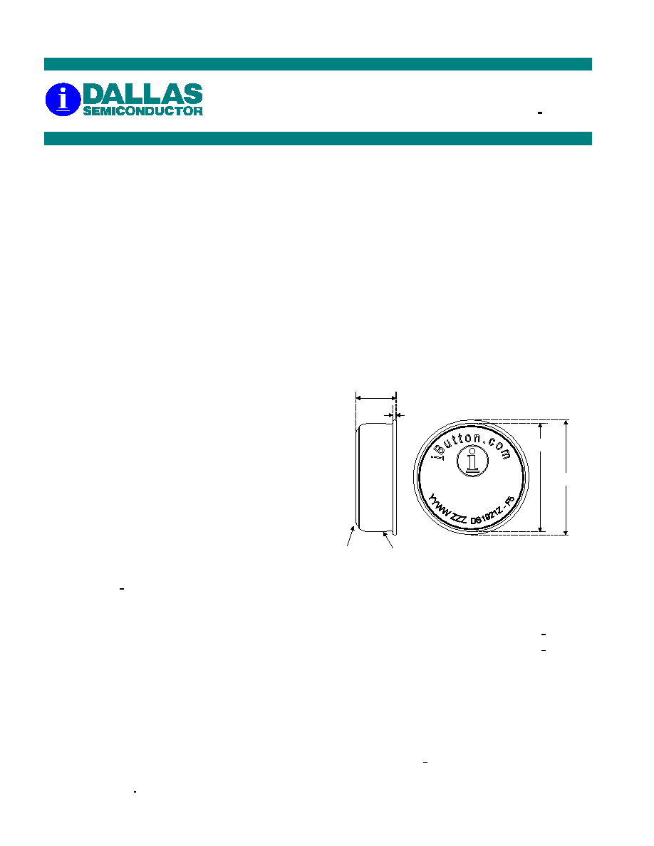
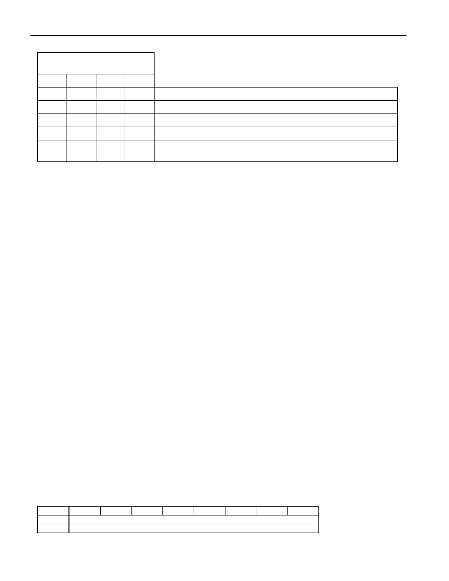
F5 MICROCAN
IO
GND
0.51
5.89
16.25
17.35
D6
21
3B2000FBC52B
1-Wire
Thermochron
Æ
All dimensions are shown in millimeters.
ORDERING INFORMATION
DS1921H-F5 +15
∞
C to +46∞C F5 iButton
Æ
DS1921Z-F5 -5
∞
C to +26∞C
F5 iButton
EXAMPLES OF ACCESSORIES
DS9096P
Self-Stick Adhesive Pad
DS9101 Multi-Purpose
Clip
DS9093RA Mounting
Lock
Ring
DS9093A Snap-In
Fob
DS9092 iButton Probe
1-Wire, Microcan, and iButton are registered trademarks of Dallas Semiconductor.

DS1921H/Z
iButton DESCRIPTION
The DS1921H/Z ThermochronTM iButtons are rugged, self-sufficient systems that measure temperature
and record the result in a protected memory section. The recording is done at a user-defined rate, both as
a direct storage of temperature values as well as in the form of a histogram. Up to 2048 temperature
values taken at equidistant intervals ranging from 1 to 255 minutes can be stored. The histogram provides
64 data bins with a resolution of 0.5∞C. If the temperature leaves a user-programmable range, the
DS1921H/Z will also record when this happened, for how long the temperature stayed outside the
permitted range, and if the temperature was too high or too low. Additional 512 bytes of read/write NV
memory allow storing information pertaining to the object to which the DS1921H/Z is associated. Data is
transferred serially via the 1-Wire protocol, which requires only a single data lead and a ground return.
Every DS1921H/Z is factory-lasered with a guaranteed unique electrically readable 64-bit registration
number that allows for absolute traceability. The durable stainless steel package is highly resistant to
environmental hazards such as dirt, moisture, and shock. Accessories permit the DS1921H/Z to be
mounted on almost any object, including containers, pallets, and bags.
APPLICATION
The DS1921Z is an ideal device to monitor the temperature of any object it is attached to or shipped with,
such as fresh produce, medical drugs and supplies. It is also ideal for use in refrigerators. The DS1921H
is intended for monitoring the body temperature of humans and animals and for monitoring temperature
critical processes such as curing, powder coating, and painting. Alternatively, the DS1921H can be used
for monitoring the temperature of clean rooms, and computer and equipment rooms. It can also aid in
calculating the proportional share of heating cost of each party in buildings with central heating. The
DS1921H has a fixed range of +15
∞
C to +46∞C. The DS1921Z has a fixed range of -5
∞
C to +26∞C. The
high resolution makes the DS1921H and DS1921Z suitable for scientific research and development. The
read/write NV memory can store information such as shipping manifests, dates of manufacture, or other
relevant data written as ASCII or encrypted files.
OVERVIEW
The block diagram in Figure 1 shows the relationships between the major control and memory sections of
the DS1921H/Z. The device has seven main data components: 1) 64-bit lasered ROM; 2) 256-bit scratch-
pad; 3) 4096-bit general-purpose SRAM; 4) 256-bit register page of timekeeping, control, and counter
registers; 5) 96 bytes of alarm time stamp and duration logging memory; 6) 128 bytes of histogram mem-
ory; and 7) 2048 bytes of data-logging memory. Except for the ROM and the scratchpad, all other mem-
ory is arranged in a single linear address space. All memory reserved for logging purposes, counter reg-
isters and several other registers are read-only for the user. The timekeeping and control registers are
write-protected while the device is programmed for a mission.
The hierarchical structure of the 1-Wire protocol is shown in Figure 2. The bus master must first provide
one of the seven ROM function commands: 1) Read ROM; 2) Match ROM; 3) Search ROM; 4) Condi-
tional Search ROM; 5) Skip ROM; 6) Overdrive-Skip ROM; or 7) Overdrive-Match ROM. Upon
completion of an Overdrive ROM command byte executed at standard speed, the device will enter
Overdrive mode, where all subsequent communication occurs at a higher speed. The protocol required for
these ROM function commands is described in Figure 13. After a ROM function command is
successfully executed, the memory functions become accessible and the master may provide any one of
the seven available commands. The protocol for these memory function commands is described in Figure
10. All data is read and written least significant bit first.
Thermochron is a trademark of Dallas Semiconductor.

DS1921H/Z
3 of 44
DS1921H/Z BLOCK DIAGRAM Figure 1
Internal
Timekeeping &
Control Reg. &
Counters
3V Lithium
General-Purpose
SRAM
Register Page
Alarm Time Stamp
and Duration
Logging Memory
Datalog
Memory
Histogram Memory
32.768kHz
Oscillator
Control
Logic
Temperature
Sensor
256-Bit
Scratchpad
Memory
Function
Control
ROM
Function
Control
64-Bit
Lasered
ROM
Parasite
Powered
Circuitry
1-Wire
Port
IO
PARASITE POWER
The block diagram (Figure 1) shows the parasite-powered circuitry. This circuitry "steals" power when-
ever the IO input is high. IO will provide sufficient power as long as the specified timing and voltage re-
quirements are met. The advantages of parasite power are two-fold: 1) by parasiting off this input, lithium
is conserved, and 2) if the lithium is exhausted for any reason, the ROM may still be read normally.
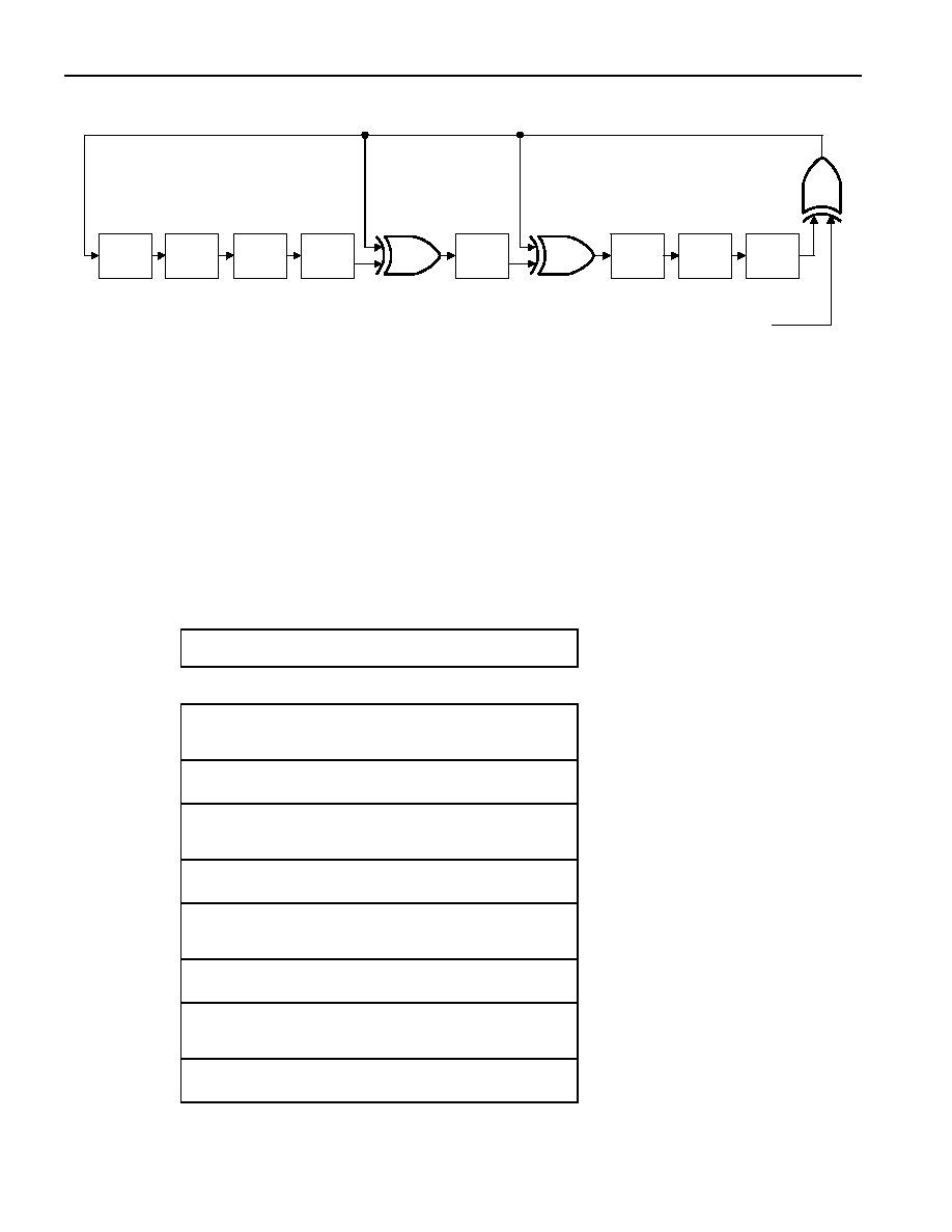
64-BIT LASERED ROM
Each DS1921 contains a unique ROM code that is 64 bits long. The first eight bits are a 1-Wire family
code. The next 36 bits are a unique serial number. The next 12 bits, called temperature range code, allow
distinguishing the DS1921H and DS1921Z from each other and from other DS1921 versions. The last
eight bits are a CRC of the first 56 bits. See Figure 3 for details. The 1-Wire CRC is generated using a
polynomial generator consisting of a shift register and XOR gates as shown in Figure 4. The polynomial
is X
8
+ X
5
+ X
4
+ 1. Additional information about the Dallas 1-Wire Cyclic Redundancy Check is avail-
able in Application Note 27 and in the Book of DS19xx iButton Standards.
The shift register bits are initialized to 0. Then starting with the least significant bit of the family code,
one bit at a time is shifted in. After the eighth
bit of the family code has been entered, then the serial
number followed by the temperature range code is entered. After the range code has been entered, the
shift register contains the CRC value. Shifting in the eight bits of CRC returns the shift register to all 0s.

DS1921H/Z
4 of 44
HIERARCHICAL STRUCTURE FOR 1-Wire PROTOCOL Figure 2
1-Wire net
Other
Devices
Bus
Master
Command
Level:
1-Wire ROM Function
Commands
DS1921-Specific
Memory/Control
Function Commands
DS1921
Available
Commands:
Read ROM
Match ROM
Search ROM
Skip ROM
Overdrive Skip
Overdrive Match
Conditional Search
ROM
Write Scratchpad
Read Scratchpad
Copy Scratchpad
Read Memory
Read Memory w/CRC
Clear Memory
Convert Temperature
Data Field
Affected:
64-bit Reg. #
64-bit Reg. #
64-bit Reg. #
N/A
OD-Flag
64-bit Reg. #, OD-Flag
64-bit Reg. #, Cond. Search settings,
device status
256-bit scratchpad, flags
256-bit scratchpad
4096-bit SRAM, registers, flags
All memory
All memory
Mission Time Stamp, Mission Samples
Counter, Start Delay, Sample
Rate, Alarm Time Stamps and
Durations, Histogram Memory
Memory address 211h
Cmd.
Codes:
33h
55h
F0h
CCh
3Ch
69h
ECh
0Fh
AAh
55h
F0h
A5h
3Ch
44h
64-BIT LASERED ROM Figure 3
MSB
LSB
8-Bit
CRC Code
12-Bit Temperature
Range Code
36-Bit Serial Number
8-Bit Family
Code (21h)
MSB
LSB
MSB
LSB
MSB
LSB
MSB
LSB
DEVICE TEMP.
RANGE (∞C)
RESOLUTION
(
∞
∞
∞
∞
C)
TEMP. RANGE CODE
HEX.
EQUIVALENT
DS1921H-F5 +15
to
+46
0.125
0100 1111 0010
4F2
DS1921Z-F5 -5
to
+26
0.125
0011 1011 0010
3B2
DS1921H/Z
5 of 44
1-Wire CRC GENERATOR Figure 4
X
0
X
1
X
2
X
3
X
4
X
5
X
6
X
7
X
8
Polynomial = X
8
+ X
5
+ X
4
+ 1
1
st
STAGE
2
nd
STAGE
3
rd
STAGE
4
th
STAGE
6
th
STAGE
5
th
STAGE
7
th
STAGE
8
th
STAGE
INPUT DATA
MEMORY
The memory map of the DS1921H/Z is shown in Figure 5. The 4096-bit general-purpose SRAM make up
pages 0 through 15. The timekeeping, control, and counter registers fill page 16, called Register Page (see
Figure 6). Pages 17 to 19 are assigned to storing the alarm time stamps and durations. The temperature
histogram bins begin at page 64 and use up to four pages. The temperature logging memory covers pages
128 to 191. Memory pages 20 to 63, 68 to 127, and 192 to 255 are reserved for future extensions. The
scratchpad is an additional page that acts as a buffer when writing to the SRAM memory or the register
page. The memory pages 17 and higher are read-only for the user. They are written to or erased solely
under supervision of the on-chip control logic.
DS1921H/Z MEMORY MAP Figure 5
32-Byte Intermediate Storage Scratchpad
ADDRESS
0000h to
01FFh
General-Purpose SRAM (16 Pages)
Pages 0 to 15
0200h to
021Fh
32-Byte Register Page
Page 16
0220h to
027Fh
Alarm Time Stamps and Durations
Pages 17 to 19
0280h to
07FFh
(Reserved for Future Extensions)
Pages 20 to 63
0800h to
087Fh
Temperature Histogram Memory
Pages 64 to 67
0880h to
0FFFh
(Reserved for Future Extensions)
Pages 68 to 127
1000h to
17FFh
Datalog Memory (64 Pages)
Pages 128 to 191
1800h to
1FFFh
(Reserved for Future Extensions)
Pages 192 to 255
DS1921H/Z
6 of 44
DS1921H/Z REGISTER PAGE MAP Figure 6
ADDR
b7 b6 b5 b4 b3 b2 b1 b0
Function
Access*
0200h
0
10 Seconds
Single Seconds
0201h
0
10 Minutes
Single Minutes
Real-
0202h 0 12/24 20h.
AM/PM
10h.
Single Hours
Time
Clock
R/W; R/W**
0203h
0 0 0 0 0
Day
of
Week Registers
0204h
0
0
10 Date
Single Date
0205h CENT
0
0
10m.
Single
Months
0206h
10 Years
Single Years
0207h
MS
10 Seconds Alarm
Single Seconds Alarm
Real-
0208h
MM
10 Minutes Alarm
Single Minutes Alarm
Time
0209h MH 12/24 10ha.
A/P
10h.
alm.
Single Hours Alarm
Clock
Alarm
R/W; R/W**
020Ah
MD 0 0 0 0 Day
of
Week
Alarm
Registers
020Bh Temperature
Low
Alarm
Threshold Temp.
R/W; R/W**
020Ch
Temperature High Alarm Threshold
Alarms
020Dh
Number of Minutes Between Temperature Conversions
Sample
Rate
R/W; R**
020Eh
EOSC
EMCLR
0
EM
RO TLS THS TAS Control
R/W; R/W**
020Fh
(no function, reads 00h)
(N/A)
R; R**
0210h
(no function, reads 00h)
(N/A)
R; R**
0211h
Temperature Read Out (Forced Conversion)
Temp.
R; R**
0212h Low
Byte Start
R/W; R/W**
0213h High
Byte Delay
0214h
TCB
MEMCLR
MIP SIP 0 TLF THF TAF Status R/W;
R/W
0215h Minutes
0216h Hours Mission
0217h Date Time R;
R
0218h Month Stamp
0219h Year
021Ah Low
Byte Mission
021Bh Center
Byte Samples R;
R
021Ch High
Byte Counter
021Dh Low
Byte Device
021Eh Center
Byte Samples R;
R
021Fh High
Byte Counter
*The first entry in column ACCESS is valid between missions. The second entry shows the applicable
access mode while a mission is in progress.
**While a mission is in progress, these addresses can be read. The first attempt to write to these registers
(even read-only ones), however, will end the mission and overwrite selected writeable registers.
TIMEKEEPING
The RTC/alarm and calendar information is accessed by reading/writing the appropriate bytes in the
register page, address 200h to 206h. Note that some bits are set to 0. These bits will always read 0
regardless of how they are written. The contents of the time, calendar, and alarm registers are in the
Binary-Coded Decimal (BCD) format.
DS1921H/Z
7 of 44
RTC and RTC Alarm Register Bitmap
ADDR
b7 b6 b5 b4 b3 b2 b1 b0
0200h
0
10 Seconds
Single Seconds
0201h
0
10 Minutes
Single Minutes
0202h 0 12/24 20h.
AM/PM
10h.
Single Hours
0203h
0 0 0 0 0
Day
of
Week
0204h
0
0
10 Date
Single Date
0205h CENT 0
0
10m.
Single
Months
0206h
10 Years
Single Years
0207h
MS
10 Seconds Alarm
Single Seconds Alarm
0208h
MM
10 Minutes Alarm
Single Minutes Alarm
0209h MH 12/24 10ha.
A/P
10h.
alm.
Single Hours Alarm
020Ah
MD 0 0 0 0 Day
of
Week
Alarm
RTC/Calendar
The RTC of the DS1921H/Z can run in either 12-hour or 24-hour mode. Bit 6 of the Hours Register
(address 202h) is defined as the 12- or 24-hour mode select bit. When high, the 12-hour mode is selected.
In the 12-hour mode, bit 5 is the AM/PM bit with logic 1 being PM. In the 24-hour mode, bit 5 is the 20-
hour bit (20 to 23 hours).
To distinguish between the days of the week the DS1921H/Z includes a counter with a range from 1 to 7.
The assignment of counter value to the day of week is arbitrary. Typically, the number 1 is assigned to a
Sunday (U.S. standard) or to a Monday (European standard).
The calendar logic is designed to automatically compensate for leap years. For every year value that is
either 00 or a multiple of 4 the device will add a 29
th
of February. This will work correctly up to (but not
including) the year 2100.
The DS1921H/Z is Y2K-compliant. Bit 7 (CENT) of the Months Register at address 205h serves as a
century flag. When the Year Register rolls over from 99 to 00 the century flag will toggle. It is recom-
mended to write the century bit to a 1 when setting the RTC to a time/date between the years 2000 and
2099.
RTC Alarms
The DS1921H/Z also contains a RTC alarm function. The alarm registers are located in registers 207h to
20Ah. The most significant bit of each of the alarm registers is a mask bit. When all of the mask bits are
logic 0, an alarm will occur once per week when the values stored in timekeeping registers 200h to 203h
match the values stored in the time of day alarm registers. Any alarm will set the Timer Alarm Flag
(TAF) in the device's Status Register (address 214h). The bus master may set the Search Conditions in the
Control Register (address 20Eh) to identify devices with timer alarms by means of the Conditional Search
function (see ROM Function Commands).
DS1921H/Z
8 of 44
RTC Alarm Control
ALARM REGISTER MASK BITS
(Bit 7 of 207h to 20Ah)
MS MM MH MD
1 1 1 1
Alarm
once
per
second.
0
1
1
1
Alarm when seconds match (once per minute).
0
0
1
1
Alarm when minutes and seconds match (once every hour).
0
0
0
1
Alarm when hours, minutes and seconds match (once every day).
0
0
0
0
Alarm when day, hours, minutes, and seconds match (once every
week).
TEMPERATURE CONVERSION
The DS1921H and DS1921Z measure temperatures with a resolution of 1/8
th
of a degree Celsius.
Temperature values are represented in a single byte as an unsigned binary number, which translates into a
range of 32∞C. The possible values are 0000 0000 (00h) through 1111 1111 (FFh). The codes 01h to FEh
are considered valid temperature readings. Since the DS1921H and DS1921Z have different starting
temperatures, the meaning of a binary temperature code depends on the device.
If a temperature conversion yields a temperature that is out-of-range, it will be recorded as 00h (if too
low) or FFh (if too high). Since out-of-range results are accumulated in histogram bins 0 and 63 the data
in these bins is of limited value (see the Temperature Logging and Histogram section). For this reason the
specified temperature range of the DS1921H and DS1921Z is considered to begin at code 04h and end at
code FBh, which corresponds to histogram bins 1 to 62.
With T[7..0] representing the decimal equivalent of a temperature reading, the temperature value is
calculated as
(∞C) = T[7...0] / 8 + 14.500 (DS1921H)
(∞C) = T[7...0] / 8 - 5.500 (DS1921Z)
This equation is valid for converting temperature readings stored in the datalog memory as well as for
data read from the forced temperature conversion readout Register (address 211h).
To specify the high or low temperature alarm thresholds, this equation needs to be resolved to
T[7...0] = 8 *
(∞C) -116 (DS1921H)
T[7...0] = 8 *
(∞C) + 44 (DS1921Z)
A value of 23∞C, for example, thus translates into 68 decimal or 44h for the DS1921H, and 228 decimal
or E4h for the DS1921Z. This corresponds to the binary patterns 0100 0100 and 1110 0100 respectively,
which could be written to a Temperature Alarm Register (address 020Bh and 020Ch, respectively).
Temperature Alarm Register Map
ADDR
b7 b6 b5 b4 b3 b2 b1 b0
020Bh Temperature
Low
Alarm
Threshold
020Ch
Temperature High Alarm Threshold
DS1921H/Z
9 of 44
SAMPLE RATE
The content of the Sample Rate Register (address 020Dh) determines how many minutes the temperature
conversions are apart from each other during a mission. The sample rate may be any value from 1 to 255,
coded as an unsigned 8-bit binary number. If the memory has been cleared (Status Register bit MEMCLR
= 1) and a mission is enabled (Status Register bit EM = 0), writing a non-zero value to the Sample Rate
Register will start a mission. For a full description of the correct sequence of steps to start a temperature-
logging mission see sections Missioning or Missioning Example.
Sample Rate Register Map
ADDR
b7 b6 b5 b4 b3 b2 b1 b0
020Dh Sample
Rate
CONTROL REGISTER
The DS1921H/Z is set up for its operation by writing appropriate data to its special function registers that
are located in the register page. Several functions that are controlled by a single bit only are combined
into a single byte called Control Register (address 20Eh). This register can be read and written. If the
device is programmed for a mission, writing to the Control Register will end the mission and change the
register contents.
Control Register Bitmap
ADDR
b7 b6 b5 b4 b3 b2 b1 b0
020Eh
EOSC
EMCLR
0
EM
RO TLS THS TAS
The functional assignments of the individual bits are explained in the table below. Bit 5 has no function.
It always reads 0 and cannot be written to 1.
Control Register Details
BIT DESCRIPTION
BIT(S)
DEFINITION
EOSC: Enable Oscillator
b7
This bit controls the crystal oscillator of the RTC. When set to logic 0,
the oscillator will start operation. When written to logic 1, the oscillator
will stop and the device is in a low-power data retention mode. This bit
must be 0 for normal operation. The RTC must have advanced at
least 1 second before a mission start will be accepted.
EMCLR: Memory Clear
Enable
b6
This bit needs to be set to logic 1 to enable the Clear Memory function,
which is invoked as a memory function command. The Time-Stamp,
Histogram Memory as well as the Mission Time Stamp, Mission
Samples Counter, Mission Start Delay and Sample Rate will be cleared
only if the Clear Memory command is issued with the next access to
the device. The EMCLR bit will return to 0 as the next memory function
command is executed.
EM: Enable Mission
b4
This bit controls whether the DS1921H/Z will begin a mission as soon as
the sample rate is written. To enable the device for a mission, this bit
must be 0.
RO: Rollover
Enable/Disable
b3
This bit controls whether the temperature logging memory is overwritten
with new data or whether data logging is stopped once the memory is
filled with data during a mission. Setting this bit to a 1 enables the
rollover and data logging continues at the beginning overwriting
previously collected data. Clearing this bit to 0 disables the rollover and
no further temperature values will be stored in the temperature logging
memory once it is filled with data. This will not stop the mission. The
device will continue measuring temperatures and updating the
histogram and alarm time stamps and durations.
DS1921H/Z
10 of 44
BIT DESCRIPTION
BIT(S)
DEFINITION
TLS: Temperature Low
Alarm Search
b2
If this bit is 1, the device will respond to a Conditional Search command
if during a mission the temperature has reached or is lower than the Low
Temperature Threshold stored at address 020Bh.
THS: Temperature High
Alarm Search
b1
If this bit is 1, the device will respond to a Conditional Search command
if during a mission the temperature has reached or is higher than the
High Temperature Threshold stored at address 020Ch.
TAS: Timer Alarm Search
b0
If this bit is 1, the device will respond to a Conditional Search command
if during a mission a timer alarm has occurred. Since a timer alarm
cannot be disabled, the TAF flag usually reads 1 during a mission.
Therefore it may be advisable to set the TAS bit to a 0, in most cases.
Mission Start Delay Counter
The content of the Mission Start Delay Counter determines how many minutes the device will wait before
starting the logging process. The mission start delay value is stored as unsigned 16-bit integer number at
addresses 212h (low byte) and 213h (high byte). The maximum delay is 65535 minutes, equivalent to 45
days, 12 hours, and 15 minutes.
For a typical mission, the Mission Start Delay is 0. If a mission is too long for a single DS1921H/Z to
store all temperature readings at the selected sample rate, one can use several devices, staggering the
Mission Start Delay to record the full period. In this case, the RO bit in the control register (address
020Eh) must be set to 0 to prevent overwriting of the recorded temperature log after the datalog memory
is full. See Mission Start and Logging Process description and flow chart for details.
Status Register
The Status Register holds device status information and alarm flags. The register is located at address
214h. Writing to this register will not necessarily end a mission.
Status Register Bitmap
ADDR
b7 b6 b5 b4 b3 b2 b1 b0
0214h
TCB
MEMCLR
MIP SIP 0 TLF THF TAF
The functional assignments of the individual bits are explained in the table below. The bits MIP, TLF,
THF and TAF can only be written to 0. All other bits are read-only. Bit 3 has no function.
Status Register Details
BIT DESCRIPTION
BIT(S)
DEFINITION
TCB: Temperature Core
Busy
b7
If this bit reads 0 the DS1921H/Z is currently performing a temperature
conversion, either self-initiated because of a mission being in progress
or initiated by a command when a mission is not in progress. The TCB
bit goes low just before a conversion starts and returns to high just after
the result is latched into the readout register at address 0211h.
MEMCLR: Memory
Cleared
b6
If this bit reads 1, the memory pages 17 and higher (alarm time
stamps/durations, temperature histogram, excluding datalog memory),
as well as the Mission Time Stamp, Mission Samples Counter, Mission
Start Delay and Sample Rate have been cleared to 0 from executing a
Clear Memory function command. The MEMCLR bit will return to 0 as
soon as writing a non-0 value to the Sample Rate Register starts a new
mission, provided that the EM bit is also 0. The memory has to be
cleared in order for a mission to start.

DS1921H/Z
11 of 44
BIT DESCRIPTION
BIT(S)
DEFINITION
MIP: Mission in Progress
b5
If this bit reads 1 the DS1921H/Z has been set up for a mission and this
mission is still in progress. A mission is started if the EM bit of the
Control Register (address 20Eh) is 0 and a non-zero value is written to
the Sample Rate Register, address 20Dh. The MIP bit returns from logic
1 to logic 0 when a mission is ended. A mission will end with the first
write attempt (Copy Scratchpad command) to any register in the
address range of 200h to 213h. Alternatively, a mission can be ended by
directly writing to the Status Register and setting the MIP bit to 0. The
MIP bit cannot be set to 1 by writing to the status register.
SIP: Sample in Progress
b4
If this bit reads 1 the DS1921H/Z is currently performing a temperature
conversion as part of a mission in progress. The mission samples occur
on the seconds rollover from 59 to 00. The SIP bit will change from 0 to
1 approximately 250ms before the actual temperature conversion begins
allowing the circuitry of the chip to wake-up. A temperature conversion
including a wake-up phase takes maximum 875ms. During this time
read accesses to the memory pages 17 and higher are permissible but
may reveal invalid data.
TLF: Temperature Low
Flag
b2
Logic 1 in the Temperature Low Flag bit indicates that a temperature
measurement during a mission revealed a temperature equal to or lower
than the value in the Temperature Low Threshold Register. The
Temperature Low Flag can be cleared at any time by writing this bit to 0.
This flag must be cleared before starting a new mission.
THF: Temperature High
Flag
b1
Logic 1 in the Temperature High Flag bit indicates that a temperature
measurement during a mission revealed a temperature equal to or
higher than the value in the Temperature High Threshold Register.
The Temperature High Flag can be cleared at any time by writing this bit
to 0. This flag must be cleared before starting a new mission.
TAF: Timer Alarm Flag
b0
If this bit reads 1, a RTC alarm has occurred (see section
TIMEKEEPING for details). The Timer Alarm Flag can be cleared at any
time by writing this bit to logic 0. Since the timer alarm cannot be
disabled, the TAF flag usually reads 1 during a mission. This flag should
be cleared before starting a new mission.
MISSION TIME STAMP
The Mission Time Stamp indicates the time and date of the first temperature conversion of a mission.
Subsequent temperature conversions will take place as many minutes apart from each other as specified
by the value in the Sample Rate Register. Mission samples occur on minute boundaries.
Mission Time Stamp Register Bitmap
ADDR
b7 b6 b5 b4 b3 b2 b1 b0
0215h
0
10 Minutes
Single Minutes
0216h
0 12/24
20h.
AM/PM
10h.
Single Hours
0217h
0
0
10 Date
Single Date
0218h 0
0 0 10m.
Single
Months
0219h
10 Years
Single Years
MISSION SAMPLES COUNTER
The Mission Samples Counter indicates how many temperature measurements have taken place during
the current mission in progress (if MIP = 1) or during the latest mission (if MIP = 0). The value is stored
as an unsigned 24-bit integer number. This counter is reset through the Clear Memory command.

DS1921H/Z
12 of 44
Mission Samples Counter Register Map
ADDR
b7 b6 b5 b4 b3 b2 b1 b0
021Ah Low
Byte
021Bh Center
Byte
021Ch High
Byte
DEVICE SAMPLES COUNTER
The Device Samples Counter indicates how many temperature measurements have taken place since the
device was assembled at the factory. The value is stored as an unsigned 24-bit integer number. The
maximum number that can be represented in this format is 16777215, which is higher than the expected
lifetime of the DS1921H/Z iButton. This counter cannot be reset under software control.
Device Samples Counter Register Map
ADDR
b7 b6 b5 b4 b3 b2 b1 b0
021Dh Low
Byte
021Eh Center
Byte
021Fh High
Byte
TEMPERATURE LOGGING AND HISTOGRAM
Once setup for a mission, the DS1921H/Z logs the temperature measurements simultaneously byte after
byte in the datalog memory as well as in histogram form in the histogram memory. The datalog memory
is able to store 2048 temperature values measured at equidistant time points. The first temperature value
of a mission is written to address location 1000h of the datalog memory, the second value to address
location 1001h and so on. Knowing the starting time point (Mission Time Stamp), the interval between
temperature measurements, the Mission Samples Counter, and the rollover setting, one can reconstruct
the time and date of each measurement stored in the datalog.
There are two alternatives to the way the DS1921H/Z will behave after the 2048 bytes of datalog memory
is filled with data. With rollover disabled (RO = 0), the device will fill the datalog memory with the first
2048 mission samples. Additional mission samples are not logged in the datalog, but the histogram, and
temperature alarm memory continue to update. With rollover enabled (RO = 1), the datalog will wrap
around, and overwrite previous data starting at 1000h for the every 2049
th
mission sample. In this mode
the device stores the last 2048 mission samples.
For the temperature histogram, the DS1921H/Z provides 64 bins that begin at memory address 0800h.
Each bin consists of a 16-bit, non-rolling-over binary counter that is incremented each time a temperature
value acquired during a mission falls into the range of the bin. The least significant byte of each bin is
stored at the lower address. Bin 0 begins at memory address 0800h, bin 1 at 0802h, and so on up to
087Eh for bin 63, as shown in Figure 7. The number of the bin to be updated after a temperature
conversion is determined by cutting off the two least significant bits of the binary temperature value. Out
of range values are range locked and counted as 00h or FFh.

DS1921H/Z
13 of 44
HISTOGRAM BIN AND TEMPERATURE CROSS-REFERENCE Figure 7
TEMPERATURE
READING
DS1921H TEMP.
EQUIV. IN ∞C
DS1921Z TEMP.
EQUIV. IN ∞C
HISTOGRAM BIN
NUMBER
HISTOGRAM BIN
ADDRESS
00h
14.500 -5.500
0 800h
to
801h
01h
14.625 -5.375
0 800h
to
801h
02h
14.750 -5.250
0 800h
to
801h
03h
14.875 -5.125
0 800h
to
801h
04h 15.000 -5.000 1 802h
to
803h
05h 15.125 -4.875 1 802h
to
803h
06h 15.250 -4.750 1 802h
to
803h
07h 15.375 -4.625 1 802h
to
803h
08h 15.500 -4.500 2 804h
to
805h
F7h 45.375 25.375 61
87Ah
to
87Bh
F8h 45.500 25.500 62
87Ch
to
87Dh
F9h 45.625 25.625 62
87Ch
to
87Dh
FAh 45.750 25.750 62
87Ch
to
87Dh
FBh 45.875 25.875 62
87Ch
to
87Dh
FCh
46.000 26.000
63 87Eh
to
87Fh
FDh
46.125 26.125
63 87Eh
to
87Fh
FEh
46.250 26.250
63 87Eh
to
87Fh
FFh
46.375 26.375
63 87Eh
to
87Fh
Since each data bin is 2 bytes it can increment up to 65535 times. Additional measurements for a bin that
has already reached its maximum value will not be counted; the bin counter will remain at its maximum
value. With the fastest sample rate of one sample every minute, a 2-byte bin is sufficient for up to 45 days
if all temperature readings fall into the same bin.
TEMPERATURE ALARM LOGGING
For some applications it may be essential to not only record temperature over time and the temperature
histogram, but also record when exactly the temperature has exceeded a predefined tolerance band and
for how long the temperature stayed outside the desirable range. The DS1921H/Z can log high and low
durations. The tolerance band is specified by means of the Temperature Alarm Threshold Registers,
addresses 20Bh and 20Ch in the register page. One can set a high and a low temperature threshold. See
section Temperature Conversion for the data format the temperature has to be written in. As long as the
temperature values stay within the tolerance band (i.e., are higher than the low threshold and lower than
the high threshold), the DS1921H/Z will not record any temperature alarm. If the temperature during a
mission reaches or exceeds either threshold, the DS1921H/Z will generate an alarm and set either the
Temperature High Flag (THF) or the Temperature Low Flag (TLF) in the Status Register (address 214h).
This way, if the search conditions (address 20Eh) are set accordingly, the master can quickly identify
devices with temperature alarms by means of the Conditional Search function (see ROM Function
Commands). The device also generates a time stamp of when the alarm occurred and begins recording the
duration of the alarming temperature.
Time stamps and durations where the temperature leaves the tolerance band are stored in the address
range 0220h to 027Fh, as shown in Figure 8. This allocation allows recording 24 individual alarm events

DS1921H/Z
14 of 44
and periods (12 periods for too hot and 12 for too cold). The date and time of each of these periods can be
determined from the Mission Time Stamp and the time distance between each temperature reading.
ALARM TIME STAMPS AND DURATIONS ADDRESS MAP Figure 8
ADDRESS DESCRIPTION
ALARM
EVENT
0220h
Mission Samples Counter Low Byte
0221h
Mission Samples Counter Center Byte
Low Alarm 1
0222h
Mission Samples Counter High Byte
0223h
Alarm Duration Counter
0224h to 0227h
Alarm Time Stamp and Duration
Low Alarm 2
0228h to 024Fh
Alarm Time Stamp and Durations
Low Alarms 3 to 12
0250h
Mission Samples Counter Low Byte
0251h
Mission Samples Counter Center Byte
High Alarm 1
0252h
Mission Samples Counter High Byte
0253h
Alarm Duration Counter
0254h to 0257h
Alarm Time Stamp and Duration
High Alarm 2
0258h to 027Fh
Alarm Time Stamp and Durations
High Alarms 3 to 12
The alarm time stamp is a copy of the Mission Samples Counter when the alarm first occurred. The least
significant byte is stored at the lower address. One address higher than the time stamp the DS1921H/Z
maintains a 1-byte duration counter that stores the number of samples the temperature was found to be
beyond the threshold. If this counter has reached its limit after 255 consecutive temperature readings and
the temperature has not yet returned to within the tolerance band, the device will issue another time stamp
at the next higher alarm location and open another counter to record the duration. If the temperature
returns to normal before the counter has reached its limit, the duration counter of the particular time
stamp will not increment any further. Should the temperature again cross this threshold, it will be
recorded at the next available alarm location. This algorithm is implemented for the low as well as for the
high temperature threshold.
MISSIONING
The typical task of the DS1921H/Z is recording the temperature of a temperature-sensitive object. Before
the device can perform this function, it needs to be configured. This procedure is called missioning.
First of all, DS1921H/Z needs to have its RTC set to valid time and date. This reference time may be
UTC (also called GMT, Greenwich Mean Time) or any other time standard that was chosen for the
application. The clock must be running (EOSC = 0) for at least one second. Setting a RTC alarm is
optional. The memory assigned to storing alarm time stamps and durations, temperature histogram, as
well as the Mission Time Stamp, Mission Samples Counter, Mission Start Delay, and Sample Rate must
be cleared using the Memory Clear command. In case there were temperature alarms in the previous
mission, the TLF and THF flags need to be cleared manually. To enable the device for a mission, the EM
flag must be set to 0. These are general settings that have to be made regardless of the type of object to be
monitored and the duration of the mission.
Next, the low temperature and high temperature thresholds to specify the temperature tolerance band
must be defined. How to convert a temperature value into the binary code to be written to the threshold
registers is described under Temperature Conversion earlier in this document.

DS1921H/Z
15 of 44
The state of the Search Condition bits in the Control Register does not affect the mission. If multiple
devices are connected to form a 1-Wire net, the setting of the search condition will enable devices to
participate in the conditional search if certain events such as timer or temperature alarm have occurred.
Details on the search conditions are found in the section ROM Function Commands later in this document
and in the Control Register description.
The setting of the RO bit (rollover enable) and sample rate depends on the duration of the mission and the
monitoring requirements. If the most recent temperature history is important, the rollover should be
enabled (RO = 1). Otherwise, one should estimate the duration of the mission in minutes and divide the
number by 2048 to calculate the value of the sample rate (number of minutes between temperature
conversions). If the estimated duration of a mission is 10 days (= 14400 minutes) for example, then the
2048-byte capacity of the datalog memory would be sufficient to store a new value every 7 minutes. If the
datalog memory of the DS1921H/Z is not large enough to store all temperature readings, one can use
several devices and set the Mission Start Delay to values that make the second device start recording as
soon as the memory of the first device is full, and so on. The RO-bit needs to be set to 0 to disable
rollover that would otherwise overwrite the recorded temperature log.
After the RO bit and the Mission Start Delay are set, the Sample Rate Register is the last element of data
that is written. The sample rate may be any value from 1 to 255, coded as an unsigned 8-bit binary
number. As soon as the sample rate is written, the DS1921H/Z will set the MIP flag and clear the
MEMCLR flag. After as many minutes as specified by the Mission Start Delay are over, the device will
wait for the next minute boundary, then wake up, copy the current time and date to the Mission Time
Stamp Register, and make the first temperature conversion of the mission. This increments both the
Mission Samples Counter and Device Samples Counter. All subsequent temperature measurements are
taken on minute boundaries specified by the value in the Sample Rate Register. One may read the
memory of the DS1921H/Z to watch the mission as it progresses. Care should be taken to avoid memory
access conflicts. See section Memory Access Conflicts for details.
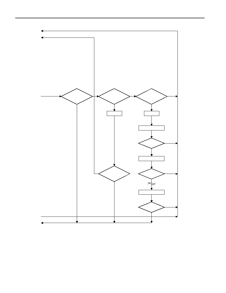
MEMORY/CONTROL FUNCTION COMMANDS
The Memory/Control Function Flow Chart (Figure 10) describes the protocols necessary for accessing
the memory and the special function registers of the DS1921H/Z. An example on how to use these and
other functions to set up the DS1921H/Z for a mission is included at the end of this document, preceding
the Electrical Characteristics section. The communication between master and DS1921H/Z takes place
either at regular speed (default, OD = 0) or at Overdrive Speed (OD = 1). If not explicitly set into the
Overdrive mode, the DS1921H/Z assumes regular speed. Internal memory access during a mission has
priority over external access through the 1-Wire interface. This can affect the Read Memory commands
described below. See section Memory Access Conflicts for details.
ADDRESS REGISTERS AND TRANSFER STATUS
Because of the serial data transfer, the DS1921H/Z employs three address registers, called TA1, TA2, and
E/S (Figure 9). Registers TA1 and TA2 must be loaded with the target address to which the data will be
written or from which data will be sent to the master upon a Read command. Register E/S acts like a byte
counter and transfer status register. It is used to verify data integrity with Write commands. Therefore, the
master only has read access to this register. The lower 5 bits of the E/S Register indicate the address of
the last byte that has been written to the scratchpad. This address is called Ending Offset. Bit 5 of the E/S
Register, called PF or "partial byte flag," is set if the number of data bits sent by the master is not an
integer multiple of 8. Bit 6 is always a 0. Note that the lowest 5 bits of the target address also determine
the address within the scratchpad, where intermediate storage of data will begin. This address is called

DS1921H/Z
16 of 44
byte offset. If the target address for a Write command is 13Ch, for example, then the scratchpad will store
incoming data beginning at the byte offset 1Ch and will be full after only 4 bytes. The corresponding
ending offset in this example is 1Fh. For best economy of speed and efficiency, the target address for
writing should point to the beginning of a new page, (i.e., the byte offset will be 0). Thus, the full 32-byte
capacity of the scratchpad is available, resulting also in the ending offset of 1Fh. However, it is possible
to write 1 or several contiguous bytes somewhere within a page. The ending offset together with the
Partial and Overflow Flag is mainly a means to support the master checking the data integrity after a
Write command. The highest valued bit of the E/S Register, called AA or Authorization Accepted,
indicates that a valid copy command for the scratchpad has been received and executed. Writing data to
the scratchpad clears this flag.
ADDRESS REGISTERS Figure 9
Bit
#
7 6 5 4 3 2 1 0
Target
Address
(TA1)
T7 T6 T5 T4 T3 T2 T1 T0
Target
Address
(TA2) T15 T14 T13 T12 T11 T10 T9 T8
Ending Address with
Data Status (E/S)
(Read Only)
AA 0 PF E4 E3 E2 E1 E0
WRITING WITH VERIFICATION
To write data to the DS1921H/Z, the scratchpad has to be used as intermediate storage. First, the master
issues the Write Scratchpad command to specify the desired target address, followed by the data to be
written to the scratchpad. In the next step, the master sends the Read Scratchpad command to read the
scratchpad and to verify data integrity. As preamble to the scratchpad data, the DS1921H/Z sends the
requested target address TA1 and TA2 and the contents of the E/S Register. If the PF flag is set, data did
not arrive correctly in the scratchpad. The master does not need to continue reading; it can start a new
trial to write data to the scratchpad. Similarly, a set AA flag indicates that the Write command was not
recognized by the device. If everything went correctly, both flags are cleared and the ending offset
indicates the address of the last byte written to the scratchpad. Now the master can continue verifying
every data bit. After the master has verified the data, it has to send the Copy Scratchpad command. This
command must be followed exactly by the data of the three address registers TA1, TA2 and E/S as the
master has read them verifying the scratchpad. As soon as the DS1921H/Z has received these bytes, it
will copy the data to the requested location beginning at the target address.
Write Scratchpad Command [0Fh]
After issuing the Write Scratchpad command, the master must first provide the 2-byte target address,
followed by the data to be written to the scratchpad. The data will be written to the scratchpad starting at
the byte offset (T4:T0). The ending offset (E4:E0) will be the byte offset at which the master stops writ-
ing data. Only full data bytes are accepted. If the last data byte is incomplete, its content will be ignored
and the partial byte flag (PF) will be set.
When executing the Write Scratchpad command, the CRC generator inside the DS1921H/Z (see Figure
16) calculates a CRC of the entire data stream, starting at the command code and ending at the last data

DS1921H/Z
17 of 44
byte sent by the master. This CRC is generated using the CRC16 polynomial by first clearing the CRC
generator and then shifting in the command code (0Fh) of the Write Scratchpad command, the Target
Addresses TA1 and TA2 as supplied by the master and all the data bytes. The master may end the Write
Scratchpad command at any time. However, if the ending offset is 11111b, the master may send 16 read
time slots and will receive an inverted CRC16 generated by the DS1921H/Z.
The range 200h to 213h of the register page is protected during a mission. See Figure 6, Register
Page Map, for the access type of the individual registers between and during missions.
Read Scratchpad Command [AAh]
This command is used to verify scratchpad data and target address. After issuing the Read Scratchpad
command, the master begins reading. The first 2 bytes will be the target address. The next byte will be the
ending offset/data status byte (E/S) followed by the scratchpad data beginning at the byte offset (T4:T0),
as shown in Figure 9. Regardless of the actual ending offset, the master may read data until the end of the
scratchpad after which it will receive an inverted CRC16 of the command code, Target Addresses TA1
and TA2, the E/S byte, and the scratchpad data starting at the target address. After the CRC is read, the
bus master will read logical 1s from the DS1921H/Z until a reset pulse is issued.
Copy Scratchpad [55h]
This command is used to copy data from the scratchpad to the writable memory sections. Applying Copy
Scratchpad to the Sample Rate Register can start a mission provided that several preconditions are met.
See Mission Start and Logging Process description and the flow chart in Figure 11 for details. After
issuing the Copy Scratchpad command, the master must provide a 3-byte authorization pattern, which can
be obtained by reading the scratchpad for verification. This pattern must exactly match the data contained
in the three address registers (TA1, TA2, E/S, in that order). If the pattern matches, the AA
(Authorization Accepted) flag will be set and the copy will begin. A pattern of alternating 1s and 0s will
be transmitted after the data has been copied until the master issues a reset pulse. While the copy is in
progress any attempt to reset the part will be ignored. Copy typically takes 2µs per byte.
The data to be copied is determined by the three address registers. The scratchpad data from the begin-
ning offset through the ending offset will be copied, starting at the target address. Anywhere from 1 to 32
bytes may be copied to memory with this command. The AA flag will remain at logic 1 until it is cleared
by the next Write Scratchpad command. Note that Copy Scratchpad when applied to the address range
200h to 213h during a mission will end the mission.
Read Memory [F0h]
The Read Memory command may be used to read the entire memory. After issuing the command, the
master must provide the 2-byte target address. After the 2 bytes, the master reads data beginning from the
target address and may continue until the end of memory, at which point logic 0s will be read. It is im-
portant to realize that the target address registers will contain the address provided. The ending offset/data
status byte is unaffected.
The hardware of the DS1921H/Z provides a means to accomplish error-free writing to the memory sec-
tion. To safeguard data in the 1-Wire environment when reading and to simultaneously speed up data
transfers, it is recommended to packetize data into data packets of the size of one memory page each.
Such a packet would typically store a 16-bit CRC with each page of data to ensure rapid, error-free data
transfers that eliminate having to read a page multiple times to verify whether if the received data is cor-
rect. (See Application Note 114 for the recommended file structure.)
DS1921H/Z
18 of 44
MEMORY/CONTROL FUNCTION FLOW CHART Figure 10-1
Master TX Memory or
Control Fkt. Command
0FH
Write
Scratchpad
DS1921 sets Scratch-
pad Offset = (T4:T0)
and Clears (PF, AA)
Master TX Data Byte
to Scratchpad Offset
DS1921 sets (E4:E0)
= Scratchpad Offset
Master
TX Reset?
Scratch-
pad Offset =
11111b?
Master RX CRC16 of
Command, Address, Data
DS1921 Incre-
ments Scratch-
pad Offset
Master RX "1"s
Master
TX Reset?
Master
TX Reset?
Partial
Byte Written?
PF = 1
AAH
Read
Scratchpad
Master RX Ending
Offset with Data
Status (E/S)
Master
TX Reset?
Scratch-
pad Offset =
11111b?
Master RX CRC16 of
Command, Address Data,
E/S Byte, and Data Starting
at the Target Address
DS1921 Incre-
ments Scratch-
pad Offset
Master RX "1"s
Master
TX Reset?
DS1921 sets Scratch-
pad Offset = (T4:T0)
Master RX Data Byte
from Scratchpad Offset
From ROM Functions
Flow Chart (Figure 12)
To ROM Functions
Flow Chart (Figure 12)
N
Y
N
Y
N
Y
N
Y
N
Y
N
Y
Y
N
Y
N
Y
N
Y
DS1921 sets
EMCLR = 0
Master TX
TA1 (T7:T0), TA2 (T15:T8)
DS1921 sets
EMCLR = 0
Master RX
TA1 (T7:T0), TA2 (T15:T8)
To Figure 10
2
nd
Part
N
From Figure 10
2
nd
Part
DS1921H/Z
19 of 44
MEMORY/CONTROL FUNCTION FLOW CHART Figure 10-2
To Figure 10
3
rd
Part
55H
Copy
Scratchpad
Master TX
E/S Byte
Authorization
Code Match?
DS1921 Copies Scratchpad
Data to Memory
Copying
Finished
Master
TX Reset?
Master
TX Reset?
AA = 1
F0H
Read
Memory
Master
TX Reset?
End of
Memory?
Master RX "0"s
DS1921 sets Memory
Address = (T15:T0)
Master RX Data Byte
from Memory Address
Master TX
TA1 (T7:T0), TA2 (T15:T8)
Master
RX "1"s
DS1921 TX "0"
DS1921 TX "1"
Master
TX Reset?
Master
RX "1"s
Master TX
TA1 (T7:T0), TA2 (T15:T8)
DS1921 Incre-
ments Address
Counter
N
Y
N
Y
N
Y
N
Y
N
Y
N
Y
N
Y
N
Y
N
Y
DS1921 sets
EMCLR = 0
DS1921 sets
EMCLR = 0
From Figure 10
1
st
Part
To Figure 10
1
st
Part
From Figure 10
3
rd
Part
DS1921H/Z
20 of 44
MEMORY/CONTROL FUNCTION FLOW CHART Figure 10-3
A5H
Read Mem.
w/CRC
DS1921 sets Memory
Address = (T15:T0)
Master RX Data Byte
from Memory Address
End of
Memory?
Y
Master
TX Reset?
CRC OK?
DS1921 Incre-
ments Address
Counter
End of Page?
Master RX CRC16 of
Command, Address, Data
(1
st
Pass); CRC16 of Data
(Subsequent Passes)
Master TX
Reset
N
Y
N
Y
Y
N
Decision made
by DS1921
Decision made
by Master
Master TX
TA1 (T7:T0), TA2 (T15:T8)
DS1921 sets
EMCLR = 0
From Figure 10
2
nd
Part
To Figure 10
2
nd
Part
To Figure 10
4
th
Part
From Figure 10
4
th
Part
N
N
Y
Master RX
00 Byte

DS1921H/Z
21 of 44
MEMORY/CONTROL FUNCTION FLOW CHART Figure 10-4
3CH
Clear
Memory
EMCLR = 1?
DS1921 clears Mission
Time Stamp, Mission
Samples Counter,
Mission Start Delay,
Sample Rate Register
DS1921 sets
EMCLR = 0
44H
Convert
Temp.
Master
TX Reset?
DS1921 Starts
Temperature
Conversion Process
Master
TX Reset?
Mission in
Progress?
N
Y
N
Y
N
Y
N
Y
N
Y
N
Y
DS1921 sets
MEMCLR = 1
DS1921 clears
Histogram Memory
DS1921 clears Alarm Time
Stamps and Durations
DS1921 sets
EMCLR = 0
Master
TX Reset?
N
Y
From Figure 10
3
rd
Part
To Figure 10
3
rd
Part
DS1921 sets
TCB\ = 0
DS1921 Performs a
Temp. Conversion
DS1921 copies Result
to Address 0211h
DS1921 sets
TCB\ = 1
Temperature Con-
version Process
End of Process

DS1921H/Z
22 of 44
Read Memory with CRC [A5h]
The Read Memory with CRC command is used to read memory data that cannot be packetized, such as
the register page and the data recorded by the device during a mission. The command works essentially
the same way as the simple Read Memory, except for the 16-bit CRC that the DS1921H/Z generates and
transmits following the last data byte of a memory page.
After having sent the command code of the Read Memory with CRC command, the bus master sends a 2-
byte address (TA1 = T7:T0, TA2 = T15:T8) that indicates a starting byte location. With the subsequent
read data time slots the master receives data from the DS1921H/Z starting at the initial address and
continuing until the end of a 32-byte page is reached. At that point the bus master will send 16 additional
read data time slots and receive an inverted 16-bit CRC. With subsequent read data time slots the master
will receive data starting at the beginning of the next page followed again by the inverted CRC for that
page. This sequence will continue until the bus master resets the device.
With the initial pass through the Read Memory with CRC flow, the 16-bit CRC value is the result of
shifting the command byte into the cleared CRC generator followed by the two address bytes and the
contents of the data memory. Subsequent passes through the Read Memory with CRC flow will generate
a 16-bit CRC that is the result of clearing the CRC generator and then shifting in the contents of the data
memory page. After the 16-bit CRC of the last page is read, the bus master will receive logical 0s from
the DS1921H/Z and inverted CRC16s at page boundaries until a reset pulse is issued. The Read Memory
with CRC command sequence can be ended at any point by issuing a reset pulse.
Clear Memory [3Ch]
The Clear Memory command is used to clear the Sample Rate, Mission Start Delay, Mission Time
Stamp, and Mission Samples Counter in the register page and the Temperature Alarm Memory and the
Temperature Histogram Memory. These memory areas must be cleared for the device to be set up for
another mission. The Clear Memory command does not clear the datalog memory or the temperature and
timer alarm flags in the Status Register. The RTC oscillator must be on and have counted at least 1
second, before issuing the command. For the Clear Memory command to function the EMCLR bit in
Control Register must be set to 1, and the Clear Memory command must be issued with the very next
access to the device's memory functions. Issuing any other memory function command will reset the
EMCLR bit. The Clear Memory process takes 500µs. When the command is completed the MEMCLR bit
in the Status Register will read 1 and the EMCLR bit will be 0.
Convert Temperature [44h]
If a mission is not in progress (MIP = 0) the Convert Temperature command can be issued to measure the
current temperature of the device. The result of the temperature conversion will be found at memory
address 211h in the register page. This command takes maximum 360ms to complete. During this time
the device remains fully accessible for memory/control and ROM function commands.

DS1921H/Z
23 of 44
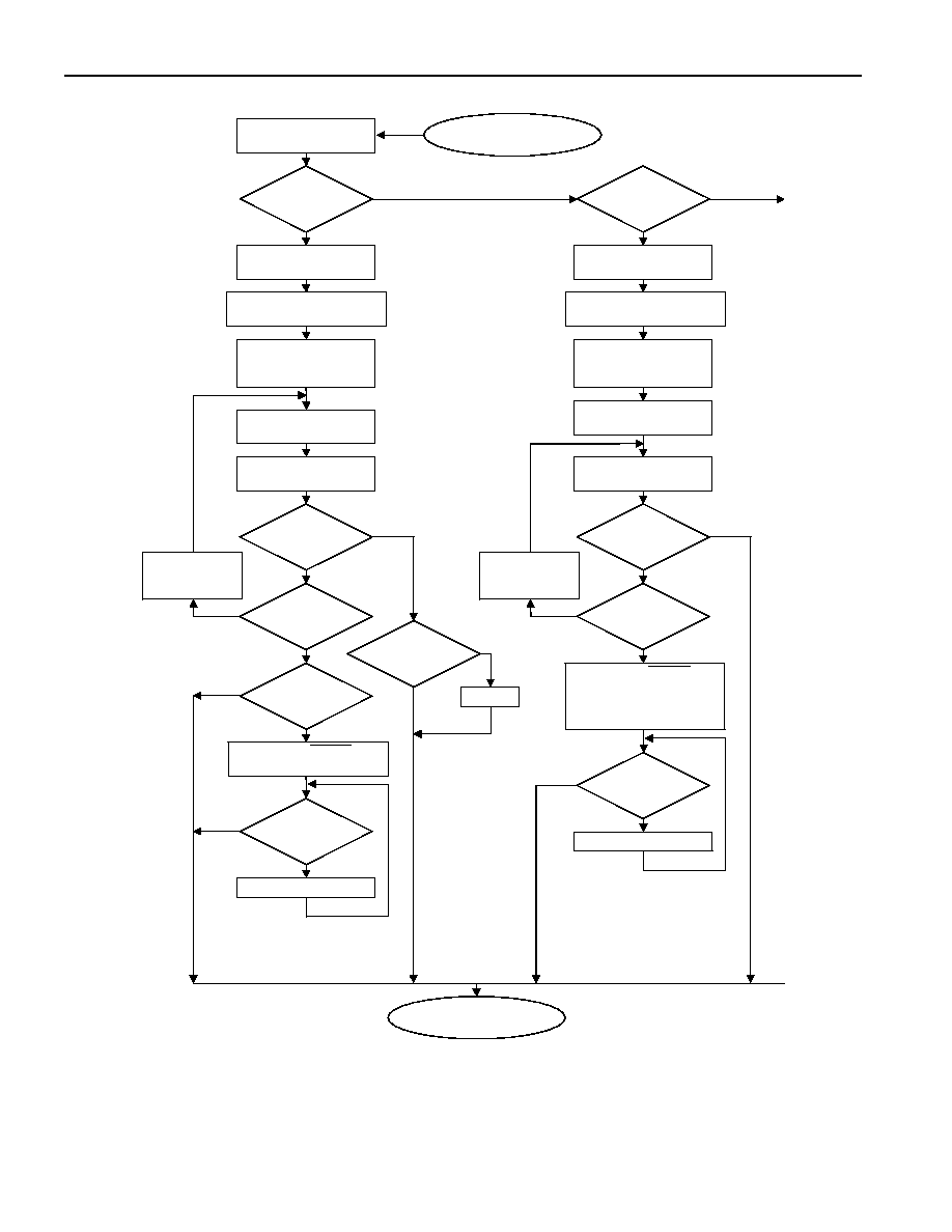
Mission Start and Logging Process
The DS1921H/Z does not use a special command to start a mission. Instead, a mission is started by
writing a non-zero value to the Sample Rate Register using the Copy Scratchpad command. As shown in
Figure 11, a new mission can only be started if the previous mission has been stopped (MIP = 0), the
memory is cleared (MEMCLR = 1) and the mission is enabled (EM = 0). If the new sample rate is
different from zero, the value will be copied to the sample rate register. At the same time the MIP bit will
be set and the MEMCLR bit will be cleared to indicate that the device is on a mission. Next the Mission
Start Delay counter will start decrementing every minute until it is down to 0. Now the DS1921H/Z will
wait until the next minute boundary and start the logging process, which as its first action copies the
applicable RTC registers to the Mission Time Stamp.
MISSION START AND LOGGING PROCESS Figure 11
The Mission Start Process is invoked when the Copy Scratchpad function is used to set a new sample rate
by writing to the Sample Rate Register at address 020Dh. One minute after the start delay countdown is
over, the Logging Process begins and the Mission Start Process ends.
Logging Process
DS1921 sets Datalog
Address = 1000h
DS1921 Measures
Temperature
DS1921 Updates His-
togram, Device Sam-
ples Counter, Mission
Samples Counter and
Alarm, if applicable
RO = 1?
DS1921 Stores Temp.
at Datalog Address
DS1921 Increments
lower 11 bits of
Datalog Address
DS1921 Stores Temp.
at Datalog Address
DS1921 Increments
Datalog Address
Datalog
Address =
1800h?
DS1921 Waits
One Sample
Period
MIP = 1?
End of Process
Y
Y
N
N
N
Y
N
DS1921 Copies new
Sample Rate from
Scratchpad to Sample
Rate Register
N
Y
N
Y
N
DS1921 sets MIP = 1;
MEMCLR = 0
MIP = 1?
MEMCLR = 1
EM = 0?
New Sample
Rate = 0?
Start Delay
Counter = 0?
Mission Start Process
DS1921 Decrements
Start Delay Counter
DS1921 Waits Until
Next Minute Boundary
DS1921 Copies RTC to
Mission Time Stamp
End of Process
DS1921 Sets MIP = 0
Y
N
Y
Y
N
MIP = 1?
Y
DS1921
Logging
Process
DS1921 Waits
Until Next
Minute
Boundary

DS1921H/Z
24 of 44
Stop Mission
The DS1921H/Z does not have a special command to stop a mission. A mission can be stopped at any
time by writing to any address in the range of 0200h to 0213h or by writing the MIP bit of the Status
Register at address 0214h to 0. Either approach involves the use of the Copy Scratchpad command. There
is no need for the Mission Start Delay to expire before a mission can be stopped (see Figure 11).
MEMORY ACCESS CONFLICTS
While a mission is in progress, periodically a temperature sample is taken and stored in the datalog, his-
togram, and potentially alarm memory. This "internal activity" has priority over a Read Memory or Read
Memory with CRC access to these pages. If a conflict occurs, the data read may be invalid, even if the
CRC value matches the data. To ensure that the data read is valid, it is recommended to first read the SIP
bit of the Status Register. If the SIP bit is set, delay reading the datalog, histogram, and alarm memory
until SIP is 0. The interference is more likely to be seen with a high sample rate (1 sample every minute).
Since all mission samples occur on the seconds rollover (59 to 00), memory conflicts can be avoided by
first reading the RTC seconds counter. For example, if it takes two seconds to read the datalog, then avoid
starting the memory read if the seconds counter is 58, 59 or 00. Alternatively, one can read the affected
memory section twice and accept the data only if both readings match. In any case, when writing driver
software, it is important to know about the possibility of interference and to take measures to work
around it.
1-WIRE BUS SYSTEM
The 1-Wire bus is a system that has a single bus master and one or more slaves. In all instances the
DS1921H/Z is a slave device. The bus master is typically a microcontroller. The discussion of this bus
system is broken down into three topics: hardware configuration, transaction sequence, and 1-Wire
signaling (signal types and timing). The 1-Wire protocol defines bus transactions in terms of the bus state
during specific time slots that are initiated on the falling edge of sync pulses from the bus master. For a
more detailed protocol description, refer to Chapter 4 of the Book of DS19xx iButton Standards.
HARDWARE CONFIGURATION
The 1-Wire bus has only a single line by definition; it is important that each device on the bus be able to
drive it at the appropriate time. To facilitate this, each device attached to the 1-Wire bus must have open
drain or tri-state outputs. The 1-Wire port of the DS1921H/Z is open-drain with an internal circuit
equivalent to that shown in Figure 12.
A multidrop bus consists of a 1-Wire bus with multiple slaves attached. At standard speed the 1-Wire bus
has a maximum data rate of 16.3kbits per second. The speed can be boosted to 142kbits per second by
activating the Overdrive mode. The DS1921H/Z is not guaranteed to be fully compliant to the iButton
Standard. Its maximum data rate in standard speed mode is 15.4kbits per second and 125kbits per second
in Overdrive. The value of the pull-up resistor primarily depends on the network size and load conditions.
The DS1921H/Z requires a pull-up resistor of maximum 2.2k
at any speed.
The idle state for the 1-Wire bus is high. If for any reason a transaction needs to be suspended, the bus
must be left in the idle state if the transaction is to resume. If this does not occur and the bus is left low
for more than 16µs (Overdrive speed) or more than 120µs (standard speed), one or more devices on the
bus may be reset. Note that the DS1921H/Z does not quite meet the full 16µs maximum low time of the
normal 1-Wire bus Overdrive timing. With the DS1921H/Z the bus must be left low for no longer than
15µs at Overdrive speed to ensure that no DS1921H/Z on the 1-Wire bus performs a reset. The
DS1921H/Z will communicate properly when used in conjunction with a DS2480B or DS2490 1-Wire
driver and adapters that are based on these driver chips.
DS1921H/Z
25 of 44
HARDWARE CONFIGURATION Figure 12
Open Drain
Port Pin
RX = RECEIVE
TX = TRANSMIT
100
MOSFET
V
PUP
RX
TX
TX
RX
DATA
5µA
Typ.
BUS MASTER
DS1921 1-Wire PORT
R
PUP
TRANSACTION SEQUENCE
The protocol for accessing the DS1921H/Z via the 1-Wire port is as follows:
Initialization
ROM Function Command
Memory/Control Function Command
Transaction/Data
INITIALIZATION
All transactions on the 1-Wire bus begin with an initialization sequence. The initialization sequence
consists of a reset pulse transmitted by the bus master followed by presence pulse(s) transmitted by the
slave(s).The presence pulse lets the bus master know that the DS1921H/Z is on the bus and is ready to
operate. For more details, see the 1-Wire Signaling section.
ROM FUNCTION COMMANDS
Once the bus master has detected a presence, it can issue one of the seven ROM function commands. All
ROM function commands are eight bits long. A list of these commands follows (refer to flowchart in
Figure 13).
Read ROM [33h]
This command allows the bus master to read the DS1921H/Z's 8-bit family code, temperature range code,
plus unique 36-bit serial number and 8-bit CRC. This command can only be used if there is a single slave
on the bus. If more than one slave is present on the bus, a data collision will occur when all slaves try to
transmit at the same time (open drain will produce a wired-AND result). The resultant family code and
temperature range code plus 36-bit serial number will result in a mismatch of the CRC.
Match ROM [55h]
The Match ROM command, followed by a 64-bit ROM sequence, allows the bus master to address a
specific DS1921H/Z on a multidrop bus. Only the DS1921H/Z that exactly matches the 64-bit ROM
sequence will respond to the following memory function command. All other slaves will wait for a reset
pulse. This command can be used with a single or multiple devices on the bus.

DS1921H/Z
26 of 44
Search ROM [F0h]
When a system is initially brought up, the bus master might not know the number of devices on the 1-
Wire bus or their registration numbers. By taking advantage of the wired-AND property of the bus, the
master can use a process of elimination to identify the registration numbers of all slave devices. For each
bit of the registration number, starting with the least significant bit, the bus master issues a triplet of time
slots. On the first slot, each slave device participating in the search outputs the true value of its
registration number bit. On the second slot, each slave device participating in the search outputs the
complemented value of its registration number bit. On the third slot, the master writes the true value of
the bit to be selected. All slave devices that do not match the bit written by the master stop participating
in the search. If both of the read bits are zero, the master knows that slave devices exist with both states of
the bit. By choosing which state to write, the bus master branches in the romcode tree. After one complete
pass, the bus master knows the registration number of a single device. Additional passes identify the
registration numbers of the remaining devices. Refer to App Note 187: 1-Wire Search Algorithm for a
detailed discussion, including an example.
Conditional Search [ECh]
The Conditional Search ROM command operates similarly to the Search ROM command except that only
devices fulfilling the specified condition will participate in the search. The condition is specified by the
bit functions TAS, THS, and TLS in the Control Register, address 20Eh. The Conditional Search ROM
provides an efficient means for the bus master to determine devices on a multidrop system that have to
signal an important event, such as a temperature leaving the tolerance band. After each pass of the
conditional search that successfully determined the 64-bit ROM code for a specific device on the
multidrop bus, that particular device can be individually accessed as if a Match ROM had been issued,
since all other devices will have dropped out of the search process and will be waiting for a reset pulse.
For the conditional search, one can select any combination of the three search conditions by writing the
associated bit to a logical 1. These bits correspond directly to the flags in the Status Register of the
device. If the flag in the status register reads 1 and the corresponding bit in the Control Register is a
logical 1 too, the device will respond to the Conditional Search command. If more than one bit search
condition is selected, the first event occurring will make the device respond to the Conditional Search
command.
Skip ROM [CCh]
This command can save time in a single-drop bus system by allowing the bus master to access the
memory functions without providing the 64-bit ROM code. If more than one slave is present on the bus
and, for example, a Read command is issued following the Skip ROM command, data collision will occur
on the bus as multiple slaves transmit simultaneously (open drain pull-downs will produce a wired-AND
result).
DS1921H/Z
27 of 44
ROM FUNCTIONS FLOW CHART Figure 13-1
To Memory Functions
Flow Chart (Figure 10)
DS1921 TX Bit 63
Master TX Bit 63
DS1921 TX Bit 63
DS1921 TX Bit 1
Master TX Bit 1
DS1921 TX Bit 1
DS1921 TX Bit 0
Master TX Bit 0
DS1921 TX Bit 0
Bit 63 Match?
Bit 1 Match?
Bit 0 Match?
F0H
Search
ROM?
N
Y
N
Y
Y
N
Y
N
DS1921 TX Bit 63
Master TX Bit 63
DS1921 TX Bit 63
DS1921 TX Bit 1
Master TX Bit 1
DS1921 TX Bit 1
DS1921 TX Bit 0
Master TX Bit 0
DS1921 TX Bit 0
Bit 63 Match?
Bit 1 Match?
Bit 0 Match?
Cond. Met?
ECH
Cond. Search
ROM?
N
Y
N
Y
N
Y
Y
N
Y
N
Master TX Bit 63
Master TX Bit 1
Master TX Bit 0
Bit 63 Match?
Bit 1 Match?
Bit 0 Match?
55H
Match
ROM?
N
Y
N
Y
Y
N
Y
N
DS1921 TX
CRC Byte
DS1921 TX
Temp. Range
Code and
Serial Number
6 Bytes
DS1921 TX
Family Code
1 Byte
33H
Read
ROM?
N
Y
From Memory Functions
Flow Chart (Figure 10)
Master TX ROM
Function Command
DS1921 TX
Presence Pulse
Master TX
Reset Pulse
Short
Reset Pulse?
N
Y
OD = 0
1)
1)
1)
1)
1)
1)
1)
1)
1)
1)
1)
1)
1)
1)
1)
1)
1)
1)
1)
1)
1)
1)
1)
1)
1)
2)
1) To be transmitted or received at Overdrive speed if
OD = 1.
2) The Presence Pulse will be short if OD = 1.
From Figure 13
2
nd
Part
From Figure 13
2
nd
Part
To Figure 13
2
nd
Part
To Figure 13
2
nd
Part
DS1921H/Z
28 of 44
ROM FUNCTIONS FLOW CHART Figure 13-2
3CH
Overdrive
Skip ROM?
N
Y
Master TX Bit 63
Master TX Bit 1
Master TX Bit 0
Bit 63 Match?
Bit 1 Match?
Bit 0 Match?
69H
Overdrive
Match?
N
Y
N
Y
Y
N
Y
N
CCH
Skip
ROM?
N
Y
3)
3)
3)
3) Always to be transmitted at Overdrive speed.
OD = 1
Master TX
Reset Pulse?
Y
N
OD = 1
To Figure 13
1
st
Part
To Figure 13
1
st
Part
From Figure 13
1
st
Part
From Figure 13
1
st
Part

DS1921H/Z
29 of 44
Overdrive Skip ROM [3Ch]
On a single-drop bus this command can save time by allowing the bus master to access the
memory/control functions without providing the 64-bit ROM code. Unlike the normal Skip ROM
command, the Overdrive Skip ROM sets the DS1921H/Z in the Overdrive mode (OD = 1). All
communication following this command has to occur at Overdrive speed until a reset pulse of minimum
480µs duration resets all devices on the bus to standard speed (OD = 0).
When issued on a multidrop bus this command will set all Overdrive-supporting devices into Overdrive
mode. To subsequently address a specific Overdrive-supporting device, a reset pulse at Overdrive speed
has to be issued followed by a Match ROM or Search ROM command sequence. This will speed up the
time for the search process. If more than one slave supporting Overdrive is present on the bus and the
Overdrive Skip ROM command is followed by a Read command, data collision will occur on the bus as
multiple slaves transmit simultaneously (open-drain pull-downs will produce a wired-AND result).
Overdrive Match ROM [69h]
The Overdrive Match ROM command followed by a 64-bit ROM sequence transmitted at Overdrive
Speed allows the bus master to address a specific DS1921H/Z on a multidrop bus and to simultaneously
set it in Overdrive mode. Only the DS1921H/Z that exactly matches the 64-bit ROM sequence will
respond to the subsequent memory/control function command. Slaves already in Overdrive mode from a
previous Overdrive Skip or successful Overdrive Match command will remain in Overdrive mode. All
overdrive-capable slaves will return to standard speed at the next Reset Pulse of minimum 480µs
duration. The Overdrive Match ROM command can be used with a single or multiple devices on the bus.
1-WIRE SIGNALING
The DS1921H/Z requires strict protocols to ensure data integrity. The protocol consists of four types of
signaling on one line: Reset Sequence with Reset Pulse and Presence Pulse, Write 0, Write 1, and Read
Data. Except for the presence pulse the bus master initiates all these signals. The DS1921H/Z can
communicate at two different speeds: standard speed and Overdrive speed. If not explicitly set into the
Overdrive mode, the DS1921H/Z will communicate at standard speed. While in Overdrive mode the fast
timing applies to all waveforms.
To get from idle to active, the voltage on the 1-Wire line needs to fall from V
PUP
below the threshold V
TL
.
To get from active to idle, the voltage needs to rise from V
ILMAX
past the threshold V
TH
. The time it takes
for the voltage to make this rise is seen in Figure 14 as `
' and its duration depends on the pull-up resistor
(R
PUP
) used and capacitance of the 1-Wire network attached. The voltage V
ILMAX
is relevant for the
DS1921H/Z when determining a logical level, but not for triggering any events.
The initialization sequence required to begin any communication with the DS1921H/Z is shown in Figure
14. A Reset Pulse followed by a Presence Pulse indicates the DS1921H/Z is ready to receive data, given
the correct ROM and memory function command. If the bus master uses slew-rate control on the falling
edge, it must pull down the line for t
RSTL
+ t
F
to compensate for the edge. A t
RSTL
duration of 480µs or
longer will exit the Overdrive mode returning the device to standard speed. If the DS1921H/Z is in
Overdrive mode and t
RSTL
is no longer than 80µs, the device will remain in Overdrive mode.
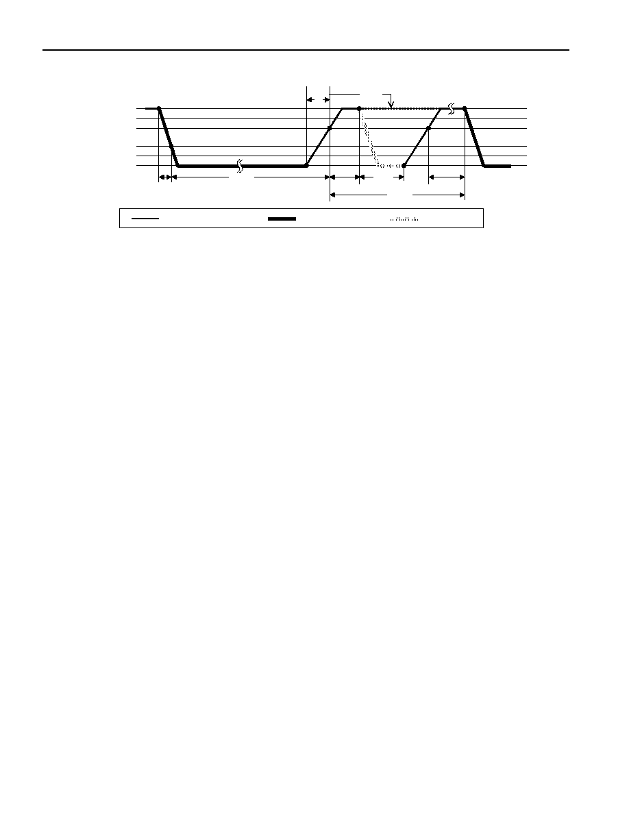
DS1921H/Z
30 of 44
INITIALIZATION PROCEDURE (RESET AND PRESENCE PULSES) Figure 14
RESISTOR
MASTER
DS1921H/Z
t
RSTL
t
PDL
t
RSTH
t
PDH
MASTER TX RESET PULSE
MASTER RX PRESENCE PULSE
V
PUP
V
IHMASTER
V
TH
V
TL
V
ILMAX
0V
t
F
t
REC
t
MSP
After the bus master has released the line it goes into receive mode (RX). Now, the 1-Wire bus is pulled
to V
PUP
via the pull-up resistor or, in case of a DS2480B driver, by active circuitry. When the threshold
V
TH
is crossed, the DS1921H/Z waits for t
PDH
and then transmits a presence pulse by pulling the line low
for t
PDL
. To detect a presence pulse, the master must test the logical state of the 1-Wire line at t
MSP
.
The t
RSTH
window must be at least the sum of t
PDHMAX
, t
PDLMAX
, and t
RECMIN
. Immediately after t
RSTH
is
expired, the DS1921H/Z is ready for data communication. In a mixed population network, t
RSTH
should
be extended to minimum 480µs at standard speed and 48µs at Overdrive speed to accommodate other 1-
Wire devices.
Read/Write Time Slots
Data communication with the DS1921H/Z takes place in time slots that carry a single bit each. Write time
slots transport data from bus master to slave. Read time-slots transfer data from slave to master. The
definitions of the write and read time slots are illustrated in Figure 15.
All communication begins with the master pulling the data line low. As the voltage on the 1-Wire line
falls below the threshold V
TL
, the DS1921H/Z starts its internal timing generator that determines when
the data line will be sampled during a write time slot and how long data will be valid during a read time
slot.
Master to Slave
For a write-one time slot, the voltage on the data line must have crossed the V
TH
threshold after the
write-one low time t
W1LMAX
is expired. For a write-zero time slot, the voltage on the data line must stay
below the V
TH
threshold until the write-zero low time t
W0LMIN
is expired. The voltage on the data line
should not exceed V
ILMAX
during the entire t
W0L
or t
W1L
window. After the V
TH
threshold has been
crossed, the DS1921H/Z needs a recovery time t
REC
before it is ready for the next time slot.
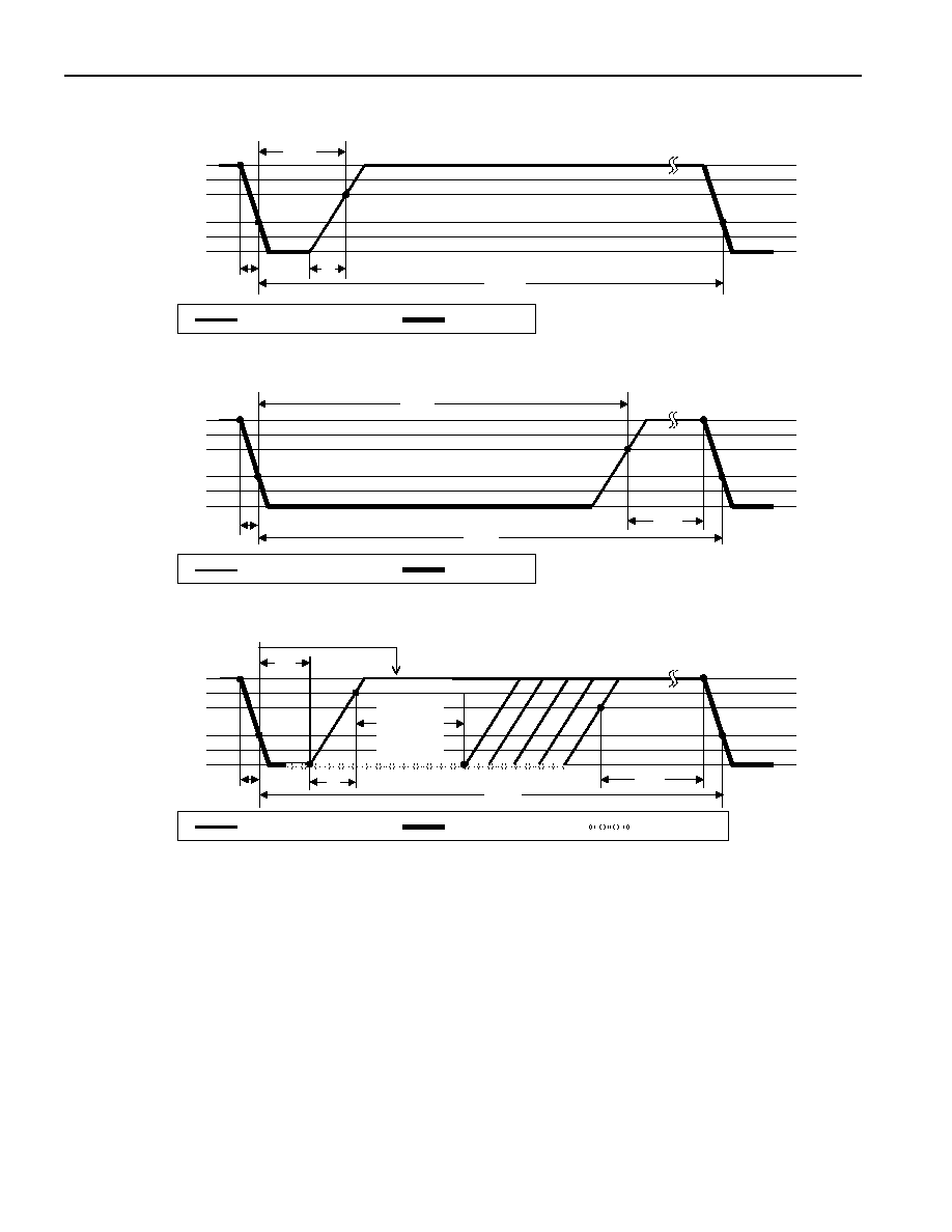
DS1921H/Z
31 of 44
READ/WRITE TIMING DIAGRAM Figure 15
Write-One Time Slot
RESISTOR
MASTER
V
PUP
V
IHMASTER
V
TH
V
TL
V
ILMAX
0V
t
F
t
SLOT
t
W1L
Write-Zero Time Slot
RESISTOR
MASTER
t
REC
V
PUP
V
IHMASTER
V
TH
V
TL
V
ILMAX
0V
t
F
t
SLOT
t
W0L
Read-Data Time Slot
RESISTOR
MASTER
DS1921H/Z
t
REC
V
PUP
V
IHMASTER
V
TH
V
TL
V
ILMAX
0V
Master
Sampling
Window
t
F
t
SLOT
t
RL
t
MSR
Slave to Master
A read-data time slot begins like a write-one time slot. The voltage on the data line must remain below
V
TL
until the read low time t
RL
is expired. During the t
RL
window, when responding with a 0, the
DS1921H/Z will start pulling the data line low; its internal timing generator determines when this pull-
down ends and the voltage starts rising again. When responding with a 1, the DS1921H/Z will not hold
the data line low at all, and the voltage starts rising as soon as t
RL
is over.
The sum of t
RL
+
(rise rime) on one side and the internal timing generator of the DS1921H/Z on the
other side define the master sampling window (t
MSRMIN
to t
MSRMAX
) in which the master must perform a
read from the data line. For most reliable communication, t
RL
should be as short as permissible and the
master should read close to but no later than t
MSRMAX
. After reading from the data line, the master must
wait until t
SLOT
is expired. This guarantees sufficient recovery time t
REC
for the DS1921H/Z to get ready
for the next time slot.

DS1921H/Z
32 of 44
CRC GENERATION
With the DS1921H/Z there are two different types of Cyclic Redundancy Checks (CRCs). One CRC is an
8-bit type and is stored in the most significant byte of the 64-bit ROM. The bus master can compute a
CRC value from the first 56 bits of the 64-bit ROM and compare it to the value stored within the
DS1921H/Z to determine if the ROM data has been received error-free. The equivalent polynomial
function of this CRC is X
8
+ X
5
+ X
4
+ 1. This 8-bit CRC is received in the true (noninverted) form. It is
computed at the factory and lasered into the ROM.
The other CRC is a 16-bit type, generated according to the standardized CRC16-polynomial function X
16
+ X
15
+ X
2
+ 1. This CRC is used for error detection when reading data memory using the Read Memory
with CRC command and for fast verification of a data transfer when writing to or reading from the
scratchpad. In contrast to the 8-bit CRC, the 16-bit CRC is always communicated in the inverted form. A
CRC-generator inside the DS1921H/Z chip (Figure 16) will calculate a new 16-bit CRC as shown in the
command flow chart of Figure 10. The bus master compares the CRC value read from the device to the
one it calculates from the data and decides whether to continue with an operation or to reread the portion
of the data with the CRC error. With the initial pass through the Read Memory with CRC flow chart, the
16-bit CRC value is the result of shifting the command byte into the cleared CRC generator, followed by
the 2 address bytes and the data bytes. Subsequent passes through the Read Memory with CRC flow chart
will generate a 16-bit CRC that is the result of clearing the CRC generator and then shifting in the data
bytes
.
With the Write Scratchpad command the CRC is generated by first clearing the CRC generator and then
shifting in the command code, the target addresses TA1 and TA2 and all the data bytes. The DS1921H/Z
will transmit this CRC only if the data bytes written to the scratchpad include scratchpad ending offset
11111b. The data may start at any location within the scratchpad.
With the Read Scratchpad command the CRC is generated by first clearing the CRC generator and then
shifting in the command code, the target addresses (TA1 and TA2), the E/S byte, and the scratchpad data
starting at the target address. The DS1921H/Z will transmit this CRC only if the reading continues
through the end of the scratchpad, regardless of the actual ending offset.
For more information on generating CRC values see Application Note 27 or the Book of DS19xx iButton
Standards.
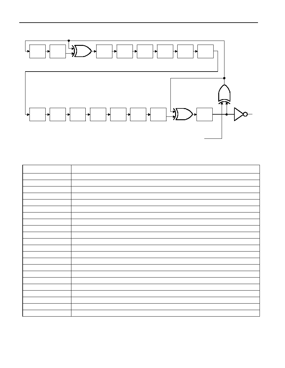
DS1921H/Z
33 of 44
CRC-16 HARDWARE DESCRIPTION AND POLYNOMIAL Figure 16
Polynomial = X
16
+ X
15
+ X
2
+ 1
X
0
X
1
X
2
X
3
X
4
X
5
X
6
X
7
X
8
X
9
X
10
X
11
X
12
X
13
X
14
X
15
X
16
1
st
STAGE
2
nd
STAGE
3
rd
STAGE
4
th
STAGE
6
th
STAGE
5
th
STAGE
7
th
STAGE
8
th
STAGE
9
th
STAGE
10
th
STAGE
11
th
STAGE
12
th
STAGE
13
th
STAGE
14
th
STAGE
15
th
STAGE
16
th
STAGE
INPUT DATA
CRC
OUTPUT
Command-Specific 1-Wire Communication Protocol -- Legend
Symbol Description
RST
1-Wire Reset Pulse generated by master
PD
1-Wire Presence Pulse generated by slave
Select
Command and data to satisfy the ROM function protocol (Skip ROM, Search ROM, etc.)
WS
Command "Write Scratchpad"
RS
Command "Read Scratchpad"
CPS
Command "Copy Scratchpad"
RM
Command "Read Memory"
RMC
Command "Read Memory with CRC"
CM
Command "Clear Memory"
CT
Command "Convert Temperature"
TA
Target Address TA1, TA2
TA-E/S
Target Address TA1, TA2 with E/S byte
<data to EOS>
Transfer of as many data bytes as are needed to reach the scratchpad offset 1Fh
<data to EOP>
Transfer of as many data bytes as are needed to reach the end of a memory page
<data to EOM>
Transfer of as many data bytes as are needed to reach the end of the datalog memory
<00 to EOP>
Transfer of as many 00h bytes as are needed to reach a memory page boundary
<32 bytes>
Transfer of 32 bytes
<data>
Transfer of an undetermined amount of data
CRC16\
Transfer of an inverted CRC16
FF loop
Indefinite loop where the master reads FFh bytes
AA loop
Indefinite loop where the master reads AAh bytes
00 loop
Indefinite loop where the master reads 00h bytes

DS1921H/Z
34 of 44
Command-Specific 1-Wire Communication Protocol -- Color Codes
Master to slave
Slave to master
Write Scratchpad, reaching the end of the Scratchpad
RST
PD
Select
WS
TA
<data to EOS> CRC16\
FF loop
Write Scratchpad, not reaching the end of the Scratchpad
RST
PD
Select
WS
TA
<data> RST
PD
Read Scratchpad
RST
PD
Select
RS
TA-E/S
<data to EOS> CRC16\
FF loop
Copy Scratchpad (success)
RST
PD
Select
CPS
TA-E/S
AA loop
Copy Scratchpad (invalid TA-E/S)
RST
PD
Select
CPS
TA-E/S
FF loop
Read Memory (success)
RST
PD
Select
RM
TA
<data to EOM> 00 loop
Read Memory (invalid address)
RST
PD
Select
RM
TA
00 loop
Reading reserved pages 20 through 63 or 68 through 127 or pages 192 and higher (beyond datalog
memory) will result in 00h bytes.
Read Memory with CRC (success)
RST
PD
Select
RMC
TA
<data to EOP> CRC16\
<32 bytes>
CRC16\
The "32 bytes" are either valid page data or 00h bytes when reading reserved pages 20 through 63 or 68
through 127 or pages 192 and higher (beyond datalog memory).
Loop
DS1921H/Z
35 of 44
Read Memory with CRC (invalid address)
RST
PD
Select
RMC
TA
<00 to EOP>
CRC16\
<32 bytes>
CRC16\
The "32 bytes" are all 00h.
Clear Memory
RST
PD
Select
CM
FF loop
To verify success, read the Status Register at address 0214h. If MEMCLR is 1, the command was
executed successfully.
Convert Temperature
RST
PD
Select
CT
FF loop
To read the result and to verify success, read the addresses 0211h (result) and the Device Samples
Coun??ter at address 021Dh to 021Fh. If the count has incremented, the command was executed
successfully.
Loop

DS1921H/Z
36 of 44
MISSION EXAMPLE: PREPARE AND START A NEW MISSION
Assumption: The previous mission has come to an end. To end an ongoing mission write the MIP bit in
the Status Register to 0.
The preparation of a DS1921H/Z for a mission including the start of the mission requires up to four steps:
Step 1: set the RTC (if it needs to be adjusted)
Step 2: clear the data of the previous mission
Step 3: set the search condition and mission start delay, clear alarm flags
Step 4: set the temperature alarms and write the sample rate to start the mission
STEP 1
Let the actual time be 15:30:00 hours on Monday, the 1
st
of April in 2002. This results in the following
data to be written to the RTC registers:
Address:
200h 201h 202h 203h 204h 205h 206h
Data: 00h 30h 15h 01h 81h 04h 02h
With only a single DS1921H/Z connected to the bus master, the communication of step 1 is as follows:
MASTER MODE
DATA (LSB FIRST)
COMMENTS
TX
(Reset)
Reset pulse (480µs to 960µs)
RX (Presence)
Presence
pulse
TX
CCh
Issue Skip ROM command
TX
0Fh
Issue Write Scratchpad command
TX
00h
TA1, beginning offset = 00h
TX
02h
TA2, address = 0200h
TX
<7 data bytes>
Write 7 bytes of data to scratchpad
TX (Reset)
Reset
pulse
RX (Presence)
Presence
pulse
TX
CCh
Issue Skip ROM command
TX
AAh
Issue Read Scratchpad command
RX
00h
Read TA1, beginning offset = 00h
RX
02h
Read TA2, address = 0200h
RX
06h
Read E/S, ending offset = 6h, flags = 0h
RX
<7 data bytes>
Read scratchpad data and verify
TX (Reset)
Reset
pulse
RX (Presence)
Presence
pulse
TX
CCh
Issue Skip ROM command
TX
55h
Issue Copy Scratchpad command
TX 00h
TX 02h
TX 06h
TA1
TA2
(AUTHORIZATION CODE)
E/S
TX (Reset)
Reset
pulse
RX (Presence)
Presence
pulse

DS1921H/Z
37 of 44
STEP 2
Set the EMCLR bit to 1, enable the RTC and then execute the Clear Memory command. The RTC
oscillator must be stable before the Clear Memory command is issued. Wait 500 µs after issuing the Clear
Memory command before proceeding to Step 3. This results in the following data to be written to the
Status Register:
Address: 20Eh
Data: 40h
With only a single DS1921H/Z connected to the bus master, the communication of step 2 is as follows:
MASTER MODE
DATA (LSB FIRST)
COMMENTS
TX
(Reset)
Reset pulse (480µs to 960µs)
RX (Presence)
Presence
pulse
TX
CCh
Issue Skip ROM command
TX
0Fh
Issue Write Scratchpad command
TX
0Eh
TA1, beginning offset = 0Eh
TX
02h
TA2, address = 020Eh
TX
40h
Write status byte to scratchpad
TX (Reset)
Reset
pulse
RX (Presence)
Presence
pulse
TX
CCh
Issue Skip ROM command
TX
AAh
Issue Read Scratchpad command
RX
0Eh
Read TA1, beginning offset = 0Eh
RX
02h
Read TA2, address = 020Eh
RX
0Eh
Read E/S, ending offset = 0Eh, flags = 0h
RX
40h
Read scratchpad data and verify
TX (Reset)
Reset
pulse
RX (Presence)
Presence
pulse
TX
CCh
Issue Skip ROM command
TX
55h
Issue Copy Scratchpad command
TX 0Eh
TX 02h
TX 0Eh
TA1
TA2
(AUTHORIZATION CODE)
E/S
TX (Reset)
Reset
pulse
RX (Presence)
Presence
pulse
TX
CCh
Issue Skip ROM command
TX
3Ch
Issue Clear Memory command
TX (Reset)
Reset
pulse
RX (Presence)
Presence
pulse

DS1921H/Z
38 of 44
STEP 3
In this example, the rollover is disabled and the search condition is set for a high temperature only. The
mission is to start with a delay of 90 (005Ah) minutes and the alarm flags TLF, THF, and TAF are
cleared. This results in the following data to be written to the special function registers:
Address:
20Eh 20Fh 210h 211h 212h 213h 214h
Data: 02h 00h* 00h* 00h* 5Ah 00h 00h
* Writing through address locations 20Fh to 211h is faster than accessing the Mission Start Delay
Register in a separate cycle. The write attempt has no effect on the contents of these registers.
With only a single DS1921H/Z connected to the bus master, the communication of step 3 is as follows:
MASTER MODE
DATA (LSB FIRST)
COMMENTS
TX
(Reset)
Reset pulse (480µs to 960µs)
RX (Presence)
Presence
pulse
TX
CCh
Issue Skip ROM command
TX
0Fh
Issue Write Scratchpad command
TX
0Eh
TA1, beginning offset = 0Eh
TX
02h
TA2, address = 020Eh
TX
<7 data bytes>
Write 7 bytes of data to scratchpad
TX (Reset)
Reset
pulse
RX (Presence)
Presence
pulse
TX
CCh
Issue Skip ROM command
TX
AAh
Issue Read Scratchpad command
RX
0Eh
Read TA1, beginning offset = 0Eh
RX
02h
Read TA2, address = 020Eh
RX
14h
Read E/S, ending offset = 14h, flags = 0h
RX
<7 data bytes>
Read scratchpad data and verify
TX (Reset)
Reset
pulse
RX (Presence)
Presence
pulse
TX
CCh
Issue Skip ROM command
TX
55h
Issue Copy Scratchpad command
TX 0Eh
TX 02h
TX 13h
TA1
TA2
(AUTHORIZATION CODE)
E/S
TX (Reset)
Reset
pulse
RX (Presence)
Presence
pulse

DS1921H/Z
39 of 44
STEP 4
In this example, the temperature alarms are set to 0
∞
C for the low temperature threshold and 10
∞
C for the
high temperature threshold, assuming it is a DS1921Z device. The sample rate is once every 10 minutes,
allowing the mission to last up to 14 days. This results in the following data to be written to the special
function registers:
Address: 20Bh 20Ch 20Dh
Data: 2Ch 7Ch 0Ah
With only a single DS1921H/Z connected to the bus master, the communication of step 4 is as follows:
MASTER MODE
DATA (LSB FIRST)
COMMENTS
TX
(Reset)
Reset pulse (480µs to 960µs)
RX (Presence)
Presence
pulse
TX
CCh
Issue Skip ROM command
TX
0Fh
Issue Write Scratchpad command
TX
0Bh
TA1, beginning offset = 0Bh
TX
02h
TA2, address = 020Bh
TX
<3 data bytes>
Write 3 bytes of data to scratchpad
TX (Reset)
Reset
pulse
RX (Presence)
Presence
pulse
TX
CCh
Issue Skip ROM command
TX
AAh
Issue Read Scratchpad command
RX
0Bh
Read TA1, beginning offset = 0Bh
RX
02h
Read TA2, address = 020Bh
RX
0Dh
Read E/S, ending offset = 0Dh, flags = 0h
RX
<3 data bytes>
Read scratchpad data and verify
TX (Reset)
Reset
pulse
RX (Presence)
Presence
pulse
TX
CCh
Issue Skip ROM command
TX
55h
Issue Copy Scratchpad command
TX 0Bh
TX 02h
TX 0Dh
TA1
TA2
(AUTHORIZATION CODE)
E/S
TX (Reset)
Reset
pulse
RX (Presence)
Presence
pulse
If step 4 was successful, the MIP bit in the Status Register will be 1, the MEMCLR bit will be 0, and the
mission start delay will be counting down.

DS1921H/Z
40 of 44
PHYSICAL SPECIFICATION
Size
See mechanical drawing
Weight 3.3g
Safety
Meets UL#913 (4
th
Edit.); Intrinsically Safe
Apparatus, approval under Entity Concept for use in
Class I, Division 1, Group A, B, C and D Locations
(application pending)
ABSOLUTE MAXIMUM RATINGS*
IO Voltage to GND
-0.5V, +6V
IO Sink Current
20mA
Temperature Range DS1921H, DS1921Z
-40∞C to +85∞C**
Storage Temperature Range
-40∞C to +50∞C**
* This is a stress rating only and functional operation of the device at these or any other conditions
above those indicated in the operation sections of this specification is not implied. Exposure to
absolute maximum rating conditions for extended periods of time may affect reliability.
** Storage or operation above 50∞C significantly reduces battery life.
ELECTRICAL CHARACTERISTICS (V
PUP
= 2.8V to 5.25V, T
A
= -40∞C to +85∞C)
PARAMETER SYMBOL CONDITIONS MIN TYP MAX
UNITS NOTES
IO pin general data
1-Wire Pull-Up
Resistance
R
PUP
2.2
k
1, 2
Input Capacitance
C
IO
100 800 pF 3,
16
Input Load Current
I
L
IO pin at V
PUP
10
µA
4
High-to-Low
V
TL
V
PUP
> 4.5V
1.14
2.70
V
5, 6, 7,
Switching Threshold
0.71
2.70
16
Input Low Voltage
V
IL
0.30
V
1, 5, 8
Low-to-High
V
TH
V
PUP
> 4.5V
1.00
2.70
V
5, 6, 9,
Switching Threshold
0.66
2.70
16
Output low voltage at
4mA
V
OL
0.4
V
5,
10
Recovery Time
t
REC
Standard Speed,
R
PUP
= 2.2k
5 µs
1,
16
Overdrive
Speed,
R
PUP
= 2.2k
2
Overdrive
Speed,
directly prior to reset
pulse; R
PUP
= 2.2k
5
Timeslot Duration
t
SLOT
Standard Speed
65
µs
1, 15
Overdrive
Speed
8
DS1921H/Z
41 of 44
PARAMETER SYMBOL CONDITIONS MIN TYP MAX
UNITS NOTES
IO pin, 1-Wire Reset, Presence Detect Cycle
Standard Speed,
V
PUP
> 4.5V
480 640
Reset Low Time
t
RSTL
Standard Speed
540
640
µs 1,
15
Overdrive
Speed
48
80
Presence Detect High
t
PDH
Standard Speed
15
60
µs
15
Time
Overdrive
Speed
1.1
6
Presence Detect Low
t
PDL
Standard Speed
60
270
µs 15
Time
Overdrive
Speed
7.5
24
Presence Detect
t
MSP
Standard Speed
60
75 µs 1,
16
Sample Time
Overdrive Speed
6
8.6
IO pin, 1-Wire Write
Write-0 Low Time
t
W0L
Standard Speed
60
120
µs
1, 15
Overdrive
Speed
6
15
Write-1 Low Time
t
W1L
Standard Speed
5
15 -
µs 1,
11
Overdrive
Speed
1
2 -
IO pin, 1-Wire Read
Read Low Time
t
RL
Standard Speed
5
15 -
µs 1,
12
Overdrive
Speed
1
2 -
Read Sample Time
t
MSR
Standard
Speed
t
RL
+
15 µs
1,
12
Overdrive
Speed
t
RL
+
2
Real-Time Clock
Frequency Deviation
F
-5∞C to +46∞C
-48
+46
PPM
Temperature Converter
Tempcore Operating
T
TC
DS1921H
15 46 ∞C
Range
DS1921Z
-5
+26
Conversion Time
t
CONV
75
360 ms
Thermal Response
Time Constant
RESP
130
s
13
Conversion Error
-1
+1
∞C
17,
18
Number of
Conversions
N
CONV
(see graphs)
--
14, 16
NOTES
1) System Requirement.
2) Maximum allowable pull-up resistance is a function of the number of 1-Wire devices in the
system and 1-Wire recovery times. The specified value here applies to systems with only one
device and with the minimum 1-Wire recovery times. For more heavily loaded systems, an active
pull-up such as that found in the DS2480B may be required.
3) Capacitance on IO could be 800pF when power is first applied. If a 2.2k
resistor is used to pull
up the data line, 2.5µs after V
PUP
has been applied the parasite capacitor will not affect normal
communication.
4) Input load is to ground.
5) All voltages are referenced to ground.
6) V
TL
, V
TH
are a function of the internal supply voltage.
7) Voltage below which, during a falling edge on IO, a logic 0 is detected.
8) The voltage on IO needs to be less or equal to V
ILMAX
whenever the master drives the line low.
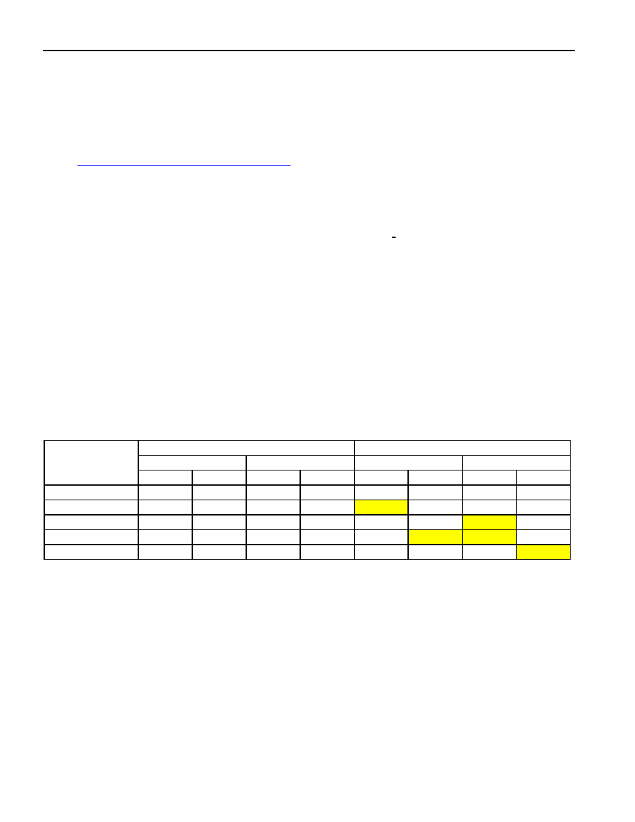
DS1921H/Z
42 of 44
9) Voltage above which, during a rising edge on IO, a logic 1 is detected.
10) The I-V characteristic is linear for voltages less than 1V.
11)
represents the time required for the pull-up circuitry to pull the voltage on IO up from V
IL
to
V
TH
.
12)
represents the time required for the pull-up circuitry to pull the voltage on IO up from V
IL
to the
input high threshold of the bus master.
13) This number was derived from a test conducted by Cemagref in Antony, France, in July of 2000.
http://www.cemagref.fr/English/index.htm
Test Report No. E42
14) The number of temperature conversions (= Samples) possible with the built-in energy source
depends on the operating and storage temperature of the device. When not in use for a mission,
the RTC oscillator should be turned off and device should be stored at a temperature not
exceeding +25∞C. Under this condition the shelf life time is 10 years minimum.
15) Highlighted numbers are not in compliance with the published iButton standards. See comparison
table below.
16) These values are derived from simulation across process, voltage, and temperature and are not
production tested.
17) Total accuracy is
plus 1/16∞C quantization due to the 1/8∞C digital resolution of the device.
18) WARNING: Not for use as the sole or primary method of measuring or tracking temperature
and/or humidity in products and articles that could affect the health or safety of persons, plants,
animals, or other living organisms, including but not limited to foods, beverages, pharmaceuticals,
medications, blood and blood products, organs, flammable, and combustible products. User shall
assure that other primary and redundant methods of testing and determining the handling
methods, quality, and fitness of the articles and products should be implemented. Temperature
and/or humidity tracking with this product is recommended only as a supplemental and redundant
information source. User shall be responsible for proper use, storage, and calibration of this
product.
Standard Values
DS1921H/Z Values
Parameter
Standard Speed
Overdrive Speed
Standard Speed
Overdrive Speed
Name
min max min max min max min max
t
SLOT
(incl. t
REC
)
61µs
(undef.) 7µs
(undef.) 65µs
1)
(undef.) 8µs
1)
(undef.)
t
RSTL
480µs (undef.)
48µs 80µs 540µs
640µs 48µs 80µs
t
PDH
15µs 60µs 2µs 6µs 15µs 60µs 1.1µs
6µs
t
PDL
60µs 240µs 8µs 24µs 60µs 270µs
7.5µs
24µs
t
W0L
60µs 120µs 6µs 16µs 60µs 120µs 6µs 15µs
1) Intentional change, longer recovery time between time slots.
DS1921H/Z
43 of 44
RTC Frequency Deviation vs Temperature
-200
-175
-150
-125
-100
-75
-50
-25
0
25
50
-40 -30 -20
-10
0
10
20
30
40
50
60
70
80
Temperature (∞C)
Fr
e
que
nc
y
D
e
v
i
a
t
i
on (
P
P
M
)
Lower Limit
Upper Limit
Minimum Product Lifetime vs Temperature at Different Sample Rates
0.00
1.00
2.00
3.00
4.00
5.00
6.00
7.00
8.00
9.00
10.00
11.00
-40 -30 -20 -10
0
10
20
30
40
50
60
70
80
Temperature (∞C)
M
i
n.
P
r
oduc
t
Li
f
e
t
i
m
e
(
y
e
a
r
s
)
Every Minute
Every 3 Min.
Every 10 Min.
No Samples
Osc. Off
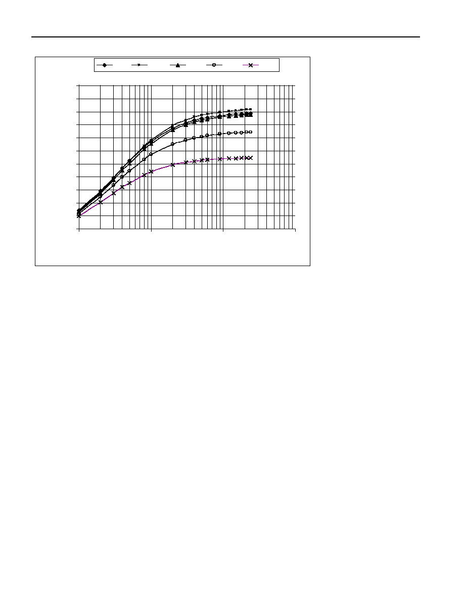
DS1921H/Z
44 of 44
Minimum Product Lifetime vs Sample Rate at Different Temperatures
1.00
2.00
3.00
4.00
5.00
6.00
7.00
8.00
9.00
10.00
11.00
12.00
1
10
100
1000
Minutes between Samples
Mi
ni
m
u
m
P
r
oduc
t
Li
f
e
t
i
m
e
(
y
e
a
r
s
)
-5∞C
15 ∞C
26∞C
37∞C
46∞C