 | –≠–ª–µ–∫—Ç—Ä–æ–Ω–Ω—ã–π –∫–æ–º–ø–æ–Ω–µ–Ω—Ç: DS2186 | –°–∫–∞—á–∞—Ç—å:  PDF PDF  ZIP ZIP |

DS2186
Transmit Line Interface
DS2186
022798 1/11
FEATURES
∑
Line interface for T1 (1.544 MHz) and CEPT (2.048
MHz) primary rate networks
∑
On≠chip transmit LBO (line build out) and line drivers
eliminate external components
∑
Programmable output pulse shape supports short≠
and long≠loop applications
∑
Supports bipolar and unipolar input data formats
∑
Transparent B8ZS and HDB3 zero code suppression
modes
∑
Compatible with DS2180A T1 and DS2181A CEPT
Transceivers DS2141A T1 and DS2143 E1 Control-
lers
∑
Companion to the DS2187 Receive Line Interface
and DS2188 T1/CEPT Jitter Attenuator
∑
Single 5V supply; low≠power CMOS technology
PIN ASSIGNMENT
LF
V
DD
V
SS
LF
20≠PIN DIP (300 MIL)
TAIS
ZCSEN
TCLKSEL
LEN0
LEN1
LEN2
TTIP
TRING
LCLK
LPOS
LNEG
TCLK
TPOS
TNEG
LB
MTIP
MRING
20
19
18
17
16
15
14
13
12
11
1
2
3
4
5
6
7
8
9
10
ZCSEN
20≠PIN SOIC (300 Mil)
1
2
3
4
5
6
7
8
9
10
20
19
18
17
16
15
14
13
12
11
LCLK
LPOS
LNEG
TCLK
TPOS
TNEG
LB
MTIP
MRING
TAIS
TCLKSEL
LEN0
LEN1
LEN2
VDD
TTIP
TRING
VSS
DESCRIPTION
The DS2186 T1/CEPT Transmit Line Interface Chip in-
terfaces user equipment to North American (T1≠1.544
MHz) and European (CEPT≠2.048 MHz) primary rate
communications networks. The device is compatible
with all types of twisted pair and coax cable found in
such networks.
Key on≠chip components include: programmable wave
shaping circuitry, line drivers, remote loopback, and
zero suppression logic. A line≠coupling transformer is
the only external component required.
Short loop (DSX≠1, 0 to 655 feet) and long loop (CSU; 0
dB, ≠7.5 dB and ≠15 dB) pulse templates found in T1
applications are supported. Appropriate CCITT recom-
mendations are met in the CEPT mode.
Application areas include DACS, CSU, CPE, channel
banks, and PABX≠to≠computer interfaces such as DMI
and CPI. The DS2186 supports ISDN≠PRI (Primary
Rate Interface) specifications.
RST
INT
CS
RAIS
LF
VDD
ZCSEN
LEN0
LEN1
LEN2
TCLKSEL
TAIS
TTIP
TRING
VSS
LCLK
LNEG
LPOS
TCLK
TPOS
TNEG
LB
MTIP
MRING
DS2186
DS2187
AVDD
LCAP
NC
ZCSEN
RCLKSEL
RTIP
RRING
LOCK
AVSS
DVDD
AIS
BPV
RCL
RPOS
RNEG
RCLK
DVSS
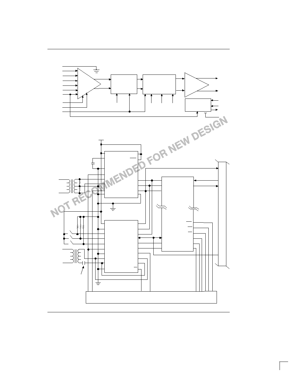
DS2180A/DS2181A
SYSTEM CONTROLLER (DS5000)
SYSTEM BACKPLANE
1.35:1
1:2
RPOS
RNEG
RCLK
TCLK
TPOS
TNEG
TSER
RSER
SCLK
SDO
SDI
RECEIVE
PAIR
TRANSMIT
PAIR
10
µ
F
0.47
µ
F
NONPOLARIZED
DS2186
022798 2/11
DS2186 BLOCK DIAGRAM Figure 1
ZERO CODE
SUPPRESSION
CIRCUITRY
WAVESHAPPING
CIRCUITRY
LINE
DRIVERS
INPUT
DATA
MUX
LINE DRIVER
MONITOR
LEN0
LEN1
LEN2
ZCSEN
TTIP
TRING
MTIP
MRING
LF
VDD
VSS
LNEG
LPOS
LCLK
TNEG
TPOS
TCLK
LB
TAIS
TCLKSEL
SYSTEM LEVEL INTERCONNECT Figure 2
DS2186
022798 3/11
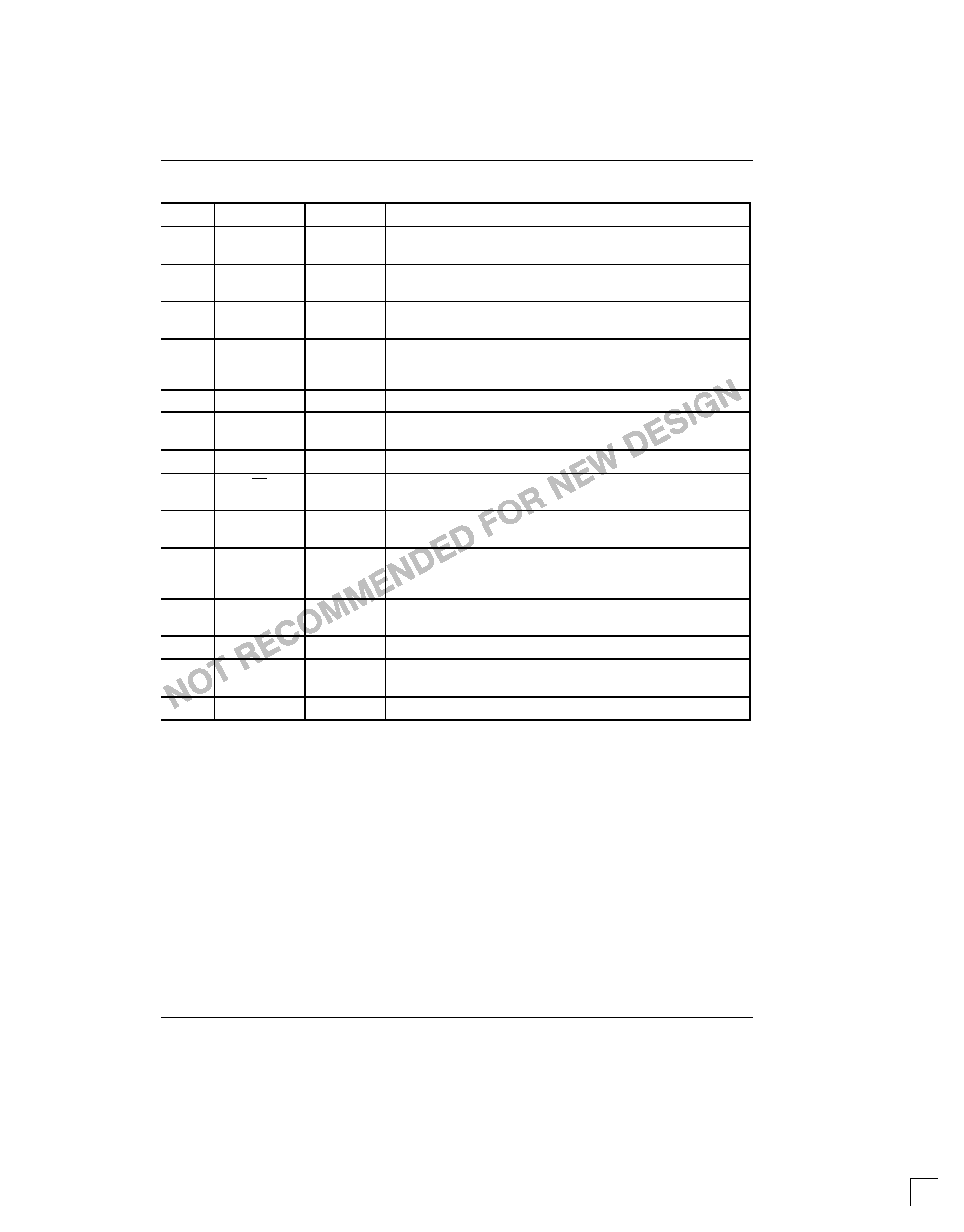
PIN DESCRIPTION Table 1
PIN
SYMBOL
TYPE
DESCRIPTION
1
TAIS
I
Transmit Alarm Indication Signal. When high, output data is
forced to all ones at the TCLK (LB=0) or LCLK (LB=1) rate.
2
ZCSEN
I
Zero Code Suppression Enable. When high, B8ZS or HDB3
encoder enabled.
3
TCLKSEL
I
Transmit Clock Select. Tie to V
SS
for 1.544 MHz (T1) applica-
tions, to V
DD
for 2.048 MHz (CEPT) applications.
4
5
6
LEN0
LEN1
LEN2
I
Length Select 0, 1 and 2. State determines output T1 waveform
shape and characteristics.
7
V
DD
≠
Positive Supply. 5.0 volts.
8
9
TTIP,
TRING
O
Transmit Tip and Ring. Line driver outputs; connect to transmit
line transformer.
10
V
SS
≠
Signal Ground. 0.0 volts.
11
LF
O
Line Fault. Open collector active low output. Held low during an
output driver fault and/or failure; tri≠stated otherwise.
12
13
MRING,
MTIP
I
Monitor Tip and Ring. Normally connected to TTIP and TRING.
Sense inputs for line fault detection circuitry.
14
LB
I
Loopback. When high, input data is sampled at LPOS and LNEG
on falling edges of LCLK; when low, input data is sampled at TPOS
and TNEG on falling TCLK.
15
16
TNEG,
TPOS
I
Transmit Data. Sampled on falling edges of TCLK when LB=0.
17
TCLK
I
Transmit Clock. 1.544 MHz or 2.048 MHz primary data clock.
18
19
LNEG,
LPOS
I
Loopback Data. Sampled on falling edges of LCLK when LB=1.
20
LCLK
I
Loopback Clock. 1.544 MHz or 2.048 MHz loopback data clock.
INPUT DATA MODES
Input data is sampled on the falling edge of TCLK or
LCLK and can be bipolar (dual rail) or unipolar (single
rail, NRZ). TPOS, TNEG and TCLK are the data and
clock inputs when LB=0, LPOS, LNEG and LCLK when
LB=1. TPOS and TNEG (LPOS and LNEG) must be tied
together in NRZ applications.
ZERO CODE SUPPRESSION MODES
Transmitted data is treated transparently (no zero code
suppression) when ZCSEN=0. HDB3 code words re-
place any all≠zero nibble when ZCSEN=1 and
TCLKSEL=1. B8ZS code words replace any incoming
all≠zero byte when ZCSEN=1 and TCLKSEL=0.
ALARM INDICATION SIGNAL
When TAIS is set, an all ones code is continuously
transmitted at the TCLK rate (LB=0) or the LCLK rate
(LB=1).
WAVE SHAPING
The device supports T1 short loop (DSX≠1; 0 to 655
feet), T1 long loop (CSU; 0 dB, ≠7.5 dB and ≠15 dB) and
CEPT (CCITT G.703) pulse template requirements.
On≠chip laser trimmed delay lines clocked by either
TCLK or LCLK control a precision digital≠to≠analog
converter to build the desired waveforms, which are
buffered differentially by the line drivers.

DS2186
022798 4/11
The shape of the "pre≠emphasized" T1 waveform is
controlled by inputs LEN0, LEN1, and LEN2
(TCLKSEL=0). These control inputs allow the user to
select the appropriate output pulse shape to meet
DSX≠1 or CSU templates over a wide variety of cable
types and lengths. Those cable types include ABAM,
PIC, and PULP.
The CEPT mode is enabled when TCLKSEL=1. Only
one output pulse shape is available in the CEPT mode;
inputs LEN0, LEN1 and LEN2 can be any state except
all zeros.
The line coupling transformer also contributes to the
pulse shape seen at the cross≠connect point. Trans-
formers for both T1 and CEPT applications must be
1:1.35.
The wave shaping circuitry does not contribute signifi-
cantly to output jitter (less than 0.01 UIpp broadband).
Output jitter will be dominated by the jitter on TCLK or
LCLK. TCLK and LCLK need only be accurate in fre-
quency, not duty cycle.
LINE DRIVERS
The on≠chip differential line drivers interface directly to
the output transformer. To optimize device perform-
ance, length of the TTIP and TRING traces should be
minimized and isolated from neighboring interconnect.
FAULT PROTECTION
The line drivers are fault≠protected and will withstand a
shorted transformer secondary (or primary) without
damage. Inputs MTIP and MRING are normally tied to
TTIP and TRING to provide fault monitoring capability.
Output LF will transition low if 192 TCLK cycles occur
without a one occurring at MTIP or MRING. LF will tri≠
state on the next one occurrence or two TCLK periods
later, whichever is greater.
The threshold of MTIP and MRING varies with the line
type selected at LEN0, LEN1 and LEN2. This insures
detection of the lowest level zero to one transition (≠15
dB buildout) as it occurs on TTIP and TRING.
T1 LINE LENGTH SELECTION Table 2
LEN2
LEN1
LEN0
OPTION SELECTED
APPLICATION
0
0
0
Test mode
Do not use
0
0
1
≠7.5 dB buildout
T1 CSU
0
1
0
≠15 dB buildout
T1 CSU
0
1
1
0 dB buildout,
0 ≠ 133 feet
T1 CSU, DSX≠1 Cross connect
1
0
0
133 ≠ 266 feet
DSX≠1 Cross connect
1
0
1
266 ≠ 399 feet
DSX≠1 Cross connect
1
1
0
399 ≠ 533 feet
DSX≠1 Cross connect
1
1
1
533 ≠ 655 feet
DSX≠1 Cross connect
NOTE:
1. The LEN0, LEN1 and LEN2 inputs control T1 output waveshapes when TCLKSEL=0. The G.703 (CEPT) template
is selected when TCLKSEL=1 and LEN0, LEN1, and LEN2 are at any state except all zeros.

DS2186
022798 5/11
DSX≠1 ISOLATED PULSE TEMPLATE Figure 3
1.0
0.5
0.0
≠0.5
0
250
500
750
1000
1250
NANOSECONDS
NORMALIZED
ALITITUDE
NOTES:
1. Template shown is measured at the cross≠connect point.
2. Amplitude shown is normalized; the actual midpoint voltage measured may be between 2.4 and 3.6 volts.
3. The corner points shown below are joined by straight lines to form the template.
MAXIMUM CURVE
MINIMUM CURVE
(0, 0.05)
(0, ≠0.05)
(250, 0.05)
(350, ≠0.05)
(325, 0.80)
(350, 0.5)
(325, 1.15)
(400, 0.95)
(425, 1.15)
(500, 0.95)
(500, 1.05)
(600, 0.9)
(675, 1.05)
(650, 0.5)
(725, ≠0.07)
(650, ≠0.45)
(875, 0.05)
(800, ≠0.45)
(1250, 0.05)
(925, ≠0.2)
(1100, ≠0.05)
(1250, ≠0.05)

DS2186
022798 6/11
OUTPUT PULSE TEMPLATE AT 2.048 MHz Figure 4
1.2
1.0
0.5
0.0
≠0.2
250
500
NANOSECONDS
NORMALIZED
AMPLITUDE
NOTES:
1. Unlike the DSX≠1 template, which is specified at the cross≠connect point, the CEPT (2.048 MHz) template is spe-
cified at the transmit line output.
2. The template shown above is normalized. The actual pulse height is cable dependent and is specified in
Table 3.
3. The corner points shown below are joined by straight lines to form the template.
MAXIMUM CURVE
MINIMUM CURVE
(0, 0.1)
(0, ≠0.1)
(109.5, 0.5)
(134.5, ≠0.2)
(109.5, 1.2)
(134.5, 0.5)
(244, 1.1)
(147, 0.8)
(378.5, 1.2)
(244, 0.9)
(378.5, 0.5)
(341, 0.8)
(488, 0.1)
(353.5, 0.5)
(353.5, ≠0.2)
(488, ≠0.1)

DS2186
022798 7/11
CHARACTERISTICS OF T1 AND CEPT INTERFACES Table 3
CHARACTERISTIC
T1
CEPT
LINE RATE
1.544 MHz
2.048 MHz
LINE CODE
AMI
1
or B8ZS
AMI or HDB3
TEST LOAD IMPEDANCE
100 ohm Resistive
120 ohm Resistive (wire pair)
75 ohm Resistive (coax)
NOMINAL PEAK
VOLTAGE
2.4V to 3.6 V
2
3.0V (wire pair)
2.37V (coax)
PULSE SHAPE
≠Scaled to fit templates shown≠
NOMINAL PULSE WIDTH
324 ns
244 ns
PULSE IMBALANCE
< 0.5 dB difference between
total power of positive and
negative pulses.
1) Negative peak = positive peak
±
5%
2) Positive width at nominal half ampli-
tude = negative width at nominal half
amplitude
±
5%.
NOTES:
1. With a ones density of at least 12.5% and no more than 15 consecutive zeros.
2. Measured at the cross≠connect (DSX≠1) point; CSU applications may be 7.5 to 15 dB below these levels.
DS2186
022798 8/11
ABSOLUTE MAXIMUM RATINGS*
Voltage on any Pin Relative to Ground
≠1.0V to +7V
Operating Temperature
0
∞
C to 70
∞
C
Storage Temperature
≠55
∞
C to +125
∞
C
Soldering Temperature
260
∞
C for 10
∞
C
* This is a stress rating only and functional operation of the device at these or any other conditions above
those indicated in the operation sections of this specification is not implied. Exposure to absolute maxi-
mum rating conditions for extended periods of time may affect reliability.
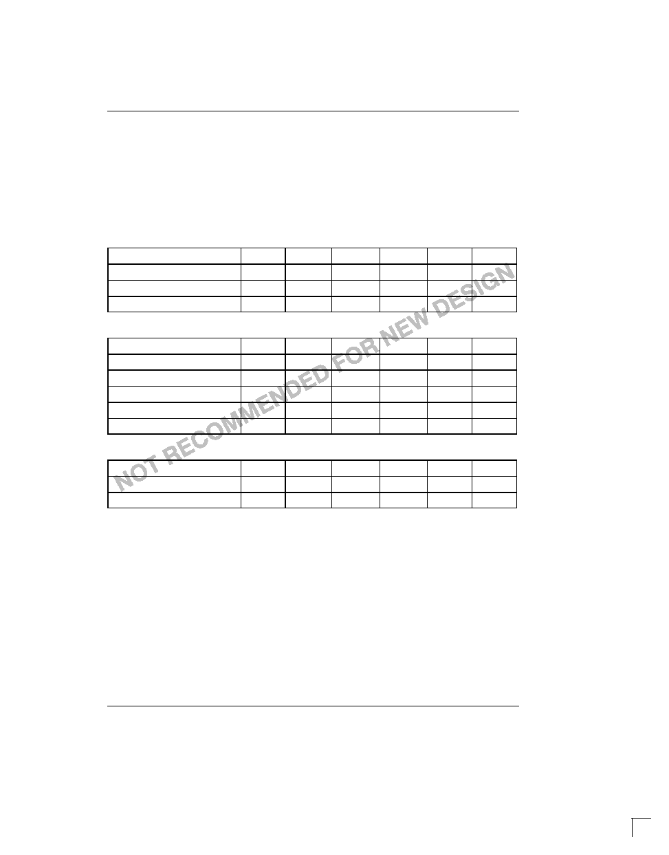
RECOMMENDED DC OPERATING CONDITIONS
(0
∞
C to 70
∞
C)
PARAMETER
SYMBOL
MIN
TYP
MAX
UNITS
NOTES
Logic 1
V
IH
2.0
V
DD
+.3
V
1
Logic 0
V
IL
≠0.3
+0.8
V
1
Supply
V
DD
4.75
5.25
V
DC ELECTRICAL CHARACTERISTICS
(0
∞
C to 70
∞
C; V
DD
= 5V
±
5%)
PARAMETER
SYMBOL
MIN
TYP
MAX
UNITS
NOTES
Supply Current
I
DD
50
mA
2,3
Supply Current
I
DD
35
mA
2,4
Supply Current
I
DD
20
mA
2,5
Input Leakage
I
IL
≠1.0
+1.0
µ
A
6
Output Current @ 0.4V
I
OL
+4.0
mA
7
CAPACITANCE
(t
A
= 25
∞
C)
PARAMETER
SYMBOL
MIN
TYP
MAX
UNITS
NOTES
Input Capacitance
C
IN
5
pF
Output Capacitance
C
OUT
7
pF
NOTES:
1. All inputs except MTIP and MRING.
2. V
DD
=5.25V; TCLK = LCLK = 1.544 MHz; output line transformer and load as shown in Figure 2.
3. TAIS = 1
4. 50% ones density.
5. All zeros at data inputs.
6. 0.0V < V
IN
< 5.0V.
7. Output LF (open collector).
DS2186
022798 9/11
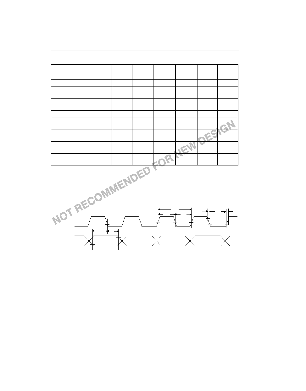
AC ELECTRICAL CHARACTERISTICS
(0
∞
C to 70
∞
C; V
DD
= 5V
±
5%)
PARAMETER
SYMBOL
MIN
TYP
MAX
UNITS
NOTES
TCLK, LCLK Period
t
CLK
648
ns
1
TCLK, LCLK Period
t
CLK
488
ns
2
TCLK, LCLK Pulse Width
t
RWH
,
t
RWL
70
324
ns
1
TCLK, LCLK Pulse Width
t
RWH
,
t
RWL
70
244
ns
2
TCLK, LCLK Rise and Fall Times
t
R
, t
F
20
ns
TPOS, TNEG Setup to TCLK
Falling
t
STD
50
ns
LPOS, LNEG Setup to LCLK
Falling
t
STD
50
ns
TPOS, TNEG Hold from TCLK
Falling
t
HTD
50
ns
LPOS, LNEG Hold from LCLK
Falling
t
HTD
50
ns
NOTES:
1. T1 applications.
2. CEPT applications.
AC TIMING DIAGRAM Figure 5
TCLK, LCLK
TPOS, TNEG
LPOS, LNEG
t
CLK
t
F
t
R
t
RWH
t
RWL
t
STD
t
HTD
DS2186
022798 10/11
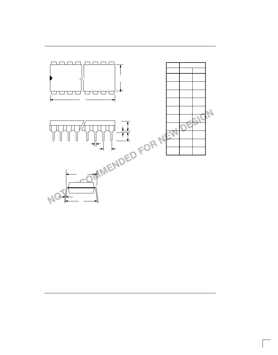
DS2186 TRANSMIT LINE INTERFACE 20≠PIN DIP
A
B
C
E
F
G
H
J
K
D
1
DIM
MIN
MAX
20≠PIN
PKG
A IN.
MM
B IN.
MM
C IN.
MM
D IN.
MM
E IN.
MM
F IN.
MM
G IN.
MM
H IN.
MM
J IN.
MM
K IN.
MM
1.020
25.91
1.040
26.42
0.240
6.10
0.260
6.60
0.120
3.05
0.140
3.56
0.300
7.62
0.325
8.26
0.015
0.38
0.040
1.02
0.120
3.04
0.140
3.56
0.090
2.23
0.110
2.79
0.320
8.13
0.370
9.40
0.008
0.20
0.012
0.30
0.015
0.38
0.021
0.53

DS2186
022798 11/11
DS2186S TRANSMIT LINE INTERFACE 20≠PIN SOIC
A
F
C
E
phi
J
G
K
L
H
B
1
DIM
MIN
MAX
20≠PIN
PKG
A IN.
MM
B IN.
MM
C IN.
MM
E IN.
MM
F IN.
MM
G IN.
MM
H IN.
MM
J IN.
MM
K IN.
MM
L IN.
MM
0.500
12.70
0.511
12.99
0.290
7.37
0.300
7.65
0.089
2.26
0.095
2.41
0.004
0.102
0.012
0.30
0.094
2.38
0.105
2.68
0.398
10.11
0.416
10.57
0.009
0.229
0.013
0.33
0.013
0.33
0.019
0.48
0.016
0.406
0.040
1.20
phi
0
∞
8
∞
0.050 BSC
1.27 BSC