 | –≠–ª–µ–∫—Ç—Ä–æ–Ω–Ω—ã–π –∫–æ–º–ø–æ–Ω–µ–Ω—Ç: DS2223 | –°–∫–∞—á–∞—Ç—å:  PDF PDF  ZIP ZIP |

DS2223/DS2224
EconoRAM
DS2223/DS2224
080598 1/10
FEATURES
∑
Low≠cost, general≠purpose, 256≠bit memory
≠ DS2223 has 256≠bit SRAM
≠ DS2224 has 32≠bit ROM, 224≠bit SRAM
∑
Reduces control, address and data interface to a
single pin
∑
Each DS2224 32≠bit ROM is factory≠lasered with a
unique serial number
∑
DS2224 portion of ROM with custom code and unique
serial number available
∑
Minimal operating power: 45 nanocoulombs per
transaction @1.5V typical
∑
Less than 15 nA standby current at 25
∞
C
∑
Nonvolatile data retention easily achieved via low≠
cost alkaline batteries or capacitors
∑
Directly connects to a port pin of popular microcontrol-
lers
∑
Operation from 1.2 to 5.5 volts
∑
Popular TO≠92 or SOT≠223 surface mount package
∑
Operates over industrial temperature range ≠40
∞
C to
+85
∞
C
DESCRIPTION
The DS2223 and DS2224 EconoRAMs are fully static,
micro≠powered, read/write memories in low≠cost
TO≠92 or SOT≠223 packages. The DS2223 is orga-
nized as a serial 256 x 1 bit static read/write memory.
The DS2224's first 32 bits are lasered with a unique ID
code at the time of manufacture; the remaining 224 bits
are static read/write memory. Signaling necessary for
reading or writing is reduced to just one interface lead.
Both the DS2223 and DS2224 are not recommended
for new designs. However, the parts will remain avail-
able until the year 2003, at least.
PACKAGE OUTLINE
1
2
3
1
2
3
1
2
3
4
SOT≠223
TOP VIEW
BOTTOM VIEW
TO≠92
See Mech. Drawings
Section
See Mech. Drawings
Section
PIN CONNECTIONS
Pin 1
GND
≠ Ground
Pin 2
DQ
≠ Data In/Out
Pin 3
V
CC
≠ Supply
Pin 4
GND
≠ Ground
ORDERING INFORMATION
DS2223
256≠bit SRAM ≠ TO≠92 Package
DS2223Z
256≠bit SRAM ≠ SOT≠223 Package
DS2223T
1000 piece tape≠and≠reel of DS2223
DS2223Y
2500 piece tape≠and≠reel of DS2223Z
DS2224
32≠bit serial number (ROM), 224≠bit
SRAM ≠ TO≠92 Package
DS2224Z
32≠bit serial number (ROM), 224≠bit
SRAM ≠ SOT≠223 Package
DS2224T
1000 piece tape≠and≠reel of DS2224
DS2224Y
2500 piece tape≠and≠reel of DS2224Z

DS2223/DS2224
080598 2/10
OPERATION
All communications to and from the EconoRAM are
accomplished via a single interface lead. EconoRAM
data is read and written through the use of time slots. All
data is preceded by a command byte to specify the type
of transaction. Once a specific transaction has been
initiated, either a read or a write, it must be com-
pleted for all memory locations before another
transaction can be started.
1≠WIRE SIGNALLING
The EconoRAM requires strict protocols to insure data
integrity. The protocol consists of three types of signal-
ling on one line: Write 0 time slot, Write 1 time slot and
Read Data time slot. All these signals are initiated by the
host.
READ/WRITE TIME SLOTS
The definitions of write and read time slots are illustrated
in Figures 1 through 3. All time slots are initiated by the
host driving the data line low. The falling edge of the data
line synchronizes the EconoRAM to the host by trigger-
ing a delay circuit in the EconoRAM. During write time
slots, the delay circuit determines when the EconoRAM
will sample the data line. For a read data time slot, if a "0"
is to be transmitted, the delay circuit determines how
long the EconoRAM will hold the data line low overriding
the 1 generated by the host. If the data bit is a "1", the
EconoRAM will leave the read data time slot
unchanged.
COMMAND BYTE
The command byte to specify the type of transaction is
transmitted LSB first from the host to the EconoRAM
using write time slots. The first bit of the command byte
(see Figure 4) is a logic 1. This indicates to the Econo-
RAM that a command byte is being written. The next two
bits are the select bits which denote the physical
address of the EconoRAM that is to be accessed (set to
00 currently). The remaining five bits determine whether
a read or a write operation is to follow. If a write operation
is to be performed, all five bits are set to a logic 1 level. If
a read operation is to be performed, any or all of these
bits are set to a logic 0 level. All eight bits of the com-
mand byte are transmitted to the EconoRAM with a sep-
arate time slot for each bit.
READ OR WRITE TRANSACTION
Read or write transactions are performed by initializing
the EconoRAM to a known state, issuing a command
byte, and then generating the time slots to either read
EconoRAM contents or write new data. Each transac-
tion consists of 264 time slots. Eight time slots transmit
the command byte, the remaining 256 time slots trans-
fer the data bits. (See Figure 5.) Once a transaction is
started, it must be completed before a new transaction
can begin.
To initially set the EconoRAM into a known state, 264
Write Zero time slots must be sent by the host. These
Write Zero time slots will not corrupt the data in the Eco-
noRAM since a command byte has not been written.
This operation will increment the address pointer inter-
nal to the EconoRAM to its maximum count value. Upon
reaching this maximum value, the EconoRAM will
ignore all additional Write Zero time slots issued to it and
the internal address pointer will remain locked at the top
count value. This condition is removed by the reception
of a Write One time slot, typically the first bit of a com-
mand byte.
Once the EconoRAM has been set into a known state,
the command byte is transmitted to the EconoRAM with
eight write time slots. This resets the address pointer
internal to the EconoRAM and prepares it for the
appropriate operation, either a read or a write.
After the command byte has been received by the Eco-
noRAM, the host controls the transfer of data. In the
case of a read transaction, the host issues 256 read time
slots. In the case of a write transaction, the host issues
256 write time slots according to the data to be written.
All data is read and written least significant bit first.
Although the DS2224 has the first 32 bits replaced by
lasered ROM rather than SRAM, it requires 256 write
time slots for a complete write transaction. The data
being sent during the first 32 write time slots has no
effect on the DS2224 other than advancing the internal
address pointer. As stated previously, it is not possible
to change from read to write or vice versa before a trans-
action is completed.

DS2223/DS2224
080598 3/10
READ/WRITE TIMING DIAGRAM
Write≠One Time Slot Figure 1
60
µ
s
t
REC
t
LOW1
V
PULLUP
V
PULLUP MIN
V
IH MIN
V
IL MAX
0V
60
µ
s < t
SLOT
<
1
1
µ
s < t
LOW1
< 15
µ
s
1
µ
s < t
REC
<
1
15
µ
s
DS2223/DS2224
SAMPLING WINDOW
t
SLOT
Write≠Zero Time Slot Figure 2
V
PULLUP
V
PULLUP MIN
V
IH MIN
V
IL MAX
0V
t
SLOT
t
REC
t
LOW0
60
µ
s < t
LOW0
< t
SLOT
<
1
1
µ
s < t
REC
<
1
DS2223/DS2224
SAMPLING WINDOW
60
µ
s
15
µ
s
Read≠Data Time Slot Figure 3
V
PULLUP
V
PULLUP MIN
V
IH MIN
V
IL MAX
0V
t
SLOT
t
REC
t
RDV
t
LOWR
60
µ
s < t
SLOT
<
1
1
µ
s < t
LOWR
< 15
µ
s
0 < t
RELEASE
< 45
µ
s
1
µ
s < t
REC
<
1
t
RDV
= 15
µ
s
t
RELEASE
HOST SAMPLING
WINDOW
RESISTOR
MASTER
DS2223/DS2224

DS2223/DS2224
080598 4/10
COMMAND WORD Figure 4
MSB
LSB
W/R
W/R
W/R
W/R
W/R
0
0
1
ALL 1s ≠ WRITE
ANY 0 ≠ READ
SELECT BITS
READ/WRITE TRANSACTION Figure 5
READ/WRITE FLOW
RECEIVE COMMAND WORD
(RESET ADDRESS POINTER)
READ/WRITE DATA BIT AND
IS ADDRESS
POINTER = 256?
HOLD ADDRESS POINTER
VALUE, WAIT FOR NEW
COMMAND WORD TO RESET
ADDRESS COUNTER
264≠BIT
TRANSACTION
8 BITS
N
Y
COMMAND WORD
COMMAND WORD
ROM
224≠BIT SRAM
256≠BIT SRAM
DS2223
DS2224
LSB
INCREMENT ADDRESS POINTER
DS2223/DS2224
080598 5/10
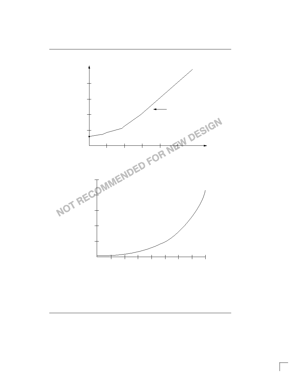
TYPICAL CURRENT CONSUMPTION VS. BIT RATE Figure 6
10
µ
A
1
µ
A
100 nA
10 nA
5 nA
129 pC/BIT
4V @ +25
∞
C
10 bps
100 bps
1 kbps
10 kbps
100 kbps
BIT RATE
CURRENT
CONSUMPTION
TYPICAL LEAKAGE CURRENT VS. TEMPERATURE Figure 7
V
CC
= 4.0V
15.0
12.0
9.0
6.0
3.0
0.0
≠10
0
+10
+20
+30
+40
+50
+60
+70
TEMPERATURE (DEG. C)
NANOAMPS
LEAKAGE CURRENT

DS2223/DS2224
080598 6/10
1≠WIRE INTERFACE
The 1≠Wire interface has only a single line by definition;
it is important that host and EconoRAM be able to drive it
at the appropriate time. The EconoRAM is an open drain
part with an internal circuit equivalent to that shown in
Figure 8. The host can be the same equivalent circuit. If
a bidirectional pin is not available, separate output and
input pins can be tied together.
The 1≠Wire interface requires a pull≠up resistor with a
value of approximately 5 k
to system V
CC
on the data
signal line. The EconoRAM has an internal open≠drain
driver with a 500 k
pull≠down resistor to ground. The
open≠drain driver allows the EconoRAM to be powered
by a small standby energy source, such as a single 1.5
volt alkaline battery, and still have the ability to produce
CMOS/TTL output levels. The pull≠down resistor holds
the DQ pin at ground when the EconoRAM is not con-
nected to the host.
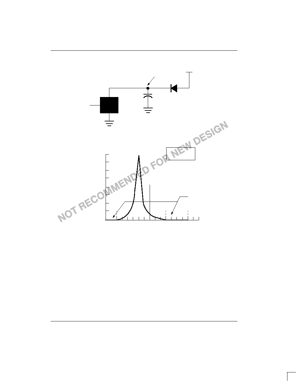
APPLICATION EXAMPLES
EconoRAMs are extremely conservative with power.
Data can be retained in these small memories for as
long as a month using the energy stored in a capacitor.
Data is retained as long as the voltage on the V
CC
pin of
the EconoRAM (V
CAP
) is at least 1.2 volts. A typical cir-
cuit is shown in Figure 9.
When V
CC
is applied, capacitor C1 is charged and the
EconoRAM receives power directly from V
CC
. After
power is removed, the diode CR1 prevents current from
leaking back into the system, keeping the capacitor
charged.
In the standby mode, the EconoRAM typically con-
sumes only 12 nA at 25
∞
C. However, the power≠down
process of the system can cause a slightly higher cur-
rent drain. This is due to the fact that as system power
ramps down, the signal attached to the DQ pin of the
EconoRAM transitions slowly through the linear region,
while the V
CAP
voltage remains at its initial value. While
in this region, the part draws more current as a function
of the DQ pin voltage (see Figure 10).
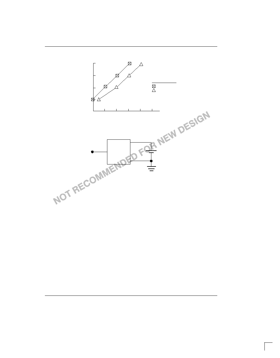
The data retention time can be estimated with the aid of
Figure 11. In this figure, the vertical axis represents the
value of the capacitor C1; the horizontal axis is the data
retention time in hours. The two curves represent initial
V
CAP
voltages of 3 and 5 volts. These curves are based
on the assumption that the time the DQ pin is in the lin-
ear region is less than 100 ms.
HOST TO ECONORAM INTERFACE Figure 8
RX
TX
TX
RX
OPEN
DRAIN
V
CC
100 OHM MOSFET
HOST
ECONORAM
500 k
V
CC
5 k
DS2223/DS2224
080598 7/10
SUGGESTED CIRCUIT Figure 9
Econo
Memory
V
CC
DQ
GND
V
CC
V
CAP
CR1
C1
+
ICC VS. DQ VOLTAGE Figure 10
V
CC
= +5V
Room Temperature
SUPPLY CURRENT
<2 nA
DQ PIN VOLTAGE
0
1
2
3
4
5
400
200
0
SUPPLY CURRENT
(
µ
A)
DS2223/DS2224
080598 8/10
DATA RETENTION TIME VS. CAPACITANCE Figure 11
10K
1K
100
10
0
0.1
1
10
100
1K
10K
TIME (hours)
Initial V
CC
Voltage
V
CC
= 3.0
V
CC
= 5.0
CAPACITANCE
(
µ
F)
Using Battery Backup
14 mA≠Hr => 144 million transactions
DS2223
DS2224
+
3
1
2
DATA
PIN
1.5V
EVEREADY
NO. 321
DS2223/DS2224
080598 9/10
ABSOLUTE MAXIMUM RATINGS*
Voltage on Any Pin Relative to Ground
≠0.5V to +6.5V
Operating Temperature
≠40
∞
C to +85
∞
C
Storage Temperature
≠55
∞
C to +125
∞
C
Soldering Temperature
260
∞
C for 10 seconds
* This is a stress rating only and functional operation of the device at these or any other conditions above
those indicated in the operation sections of this specification is not implied. Exposure to absolute maxi-
mum rating conditions for extended periods of time may affect reliability.
RECOMMENDED DC OPERATING CONDITIONS
(≠40
∞
C to +85
∞
C)
PARAMETER
SYMBOL
MIN
TYP
MAX
UNITS
NOTES
Data Pin
DQ
≠0.5
6.0
V
1
Supply Voltage
V
CC
1.2
5.5
V
1
DC ELECTRICAL CHARACTERISTICS
(≠40
∞
C to +85
∞
C; V
CC
=2.0V to 5.5V)
PARAMETER
SYMBOL
MIN
TYP
MAX
UNITS
NOTES
Input Logic Low
V
IL
≠0.5
0.4
0.8
V
1
Input Logic High
V
IH
V
CC
≠0.5
6.0
V
1
Sink Current
I
L
1
2
mA
4
Output Logic Low
V
OL
0.4
V
1
Output Logic High
V
OH
V
PUP
5.5
V
1, 2
Input Resistance
I
R
500
k
3
Operating Current
I
OP
36
nC
5
Standby Current
I
STBY
2
25
nA
6
DC ELECTRICAL CHARACTERISTICS
(≠40
∞
C to +85
∞
C; V
CC
=1.4V
±
10%)
PARAMETER
SYMBOL
MIN
TYP
MAX
UNITS
NOTES
Input Logic Low
V
IL
≠0.5
0.2
V
1
Input Logic High
V
IH
1.0
6.0
V
1
Sink Current
I
L
1
2
mA
7
Output Logic Low
V
OL
0.4
V
4
Output Logic High
V
OH
V
PUP
5.5
V
1, 2
Input Resistance
I
R
500
k
3
Operating Current
I
OP
36
nC
5
Standby Current
I
STBY
2
15
nA
6

DS2223/DS2224
080598 10/10
AC ELECTRICAL CHARACTERISTICS
(≠40
∞
C to +85
∞
C; V
CC
=1.4V
±
10%)
PARAMETER
SYMBOL
MIN
TYP
MAX
UNITS
NOTES
Time Slot
t
SLOT
70
µ
s
Read Data Valid
t
RDV
exactly 15
µ
s
Release Time
t
RELEASE
0
15
45
µ
s
Write 1 Low Time
t
LOW1
1
15
µ
s
Write 0 Low Time
t
LOW0
60
µ
s
Data Setup Time
t
SU
1
µ
s
8
Recovery Time
t
REC
1
µ
s
AC ELECTRICAL CHARACTERISTICS
(≠40
∞
C to +85
∞
C; V
CC
=2.0V to 5.5V)
PARAMETER
SYMBOL
MIN
TYP
MAX
UNITS
NOTES
Time Slot
t
SLOT
60
µ
s
Read Data Valid
t
RDV
exactly 15
µ
s
Release Time
t
RELEASE
0
15
45
µ
s
Write 1 Low Time
t
LOW1
1
15
µ
s
Write 0 Low Time
t
LOW0
60
µ
s
Data Setup Time
t
SU
1
µ
s
8
Recovery Time
t
REC
1
µ
s
NOTES:
1. All voltages are referenced to ground.
2. V
PUP
= external pull≠up voltage to system sypply.
3. Input pull≠down resistance to ground.
4. @ V
OL
=0.4V
5. 36 nanocoulombs per 264 time slots @ 1.5V (see Figure 6).
6. See Figure 7 for typical values over temperature.
7. @ V
OL
=0.2V
8. Read data setup time refers to the time the host must pull the 1≠Wire line low to read a bit. Data is guaran-
teed to be valid within 1
µ
s of this falling edge and will remain valid for 14
µ
s minimum (15
µ
s total from falling
edge on the 1≠Wire line).