 | –≠–ª–µ–∫—Ç—Ä–æ–Ω–Ω—ã–π –∫–æ–º–ø–æ–Ω–µ–Ω—Ç: DS2422 | –°–∫–∞—á–∞—Ç—å:  PDF PDF  ZIP ZIP |
1 of 48
REV: 111403
Note: Some revisions of this device may incorporate deviations from published specifications known as errata. Multiple revisions of any device
may be simultaneously available through various sales channels. For information about device errata, click here:
www.maxim-ic.com/errata
.
GENERAL DESCRIPTION
The DS2422 temperature/datalogger combines the
core functions of a fully featured datalogger in a
single chip. It includes a temperature sensor, real-
time clock (RTC), memory, 1-Wire
Æ
interface, and
serial interface for an analog-to-digital converter
(ADC) as well as control circuitry for a charge pump.
The ADC and the charge pump are peripherals that
can be added to build application-specific
dataloggers. Without external ADC, the DS2422
functions as a temperature logger only. The DS2422
measures the temperature and/or reads the ADC at a
user-defined rate. A total of 8192 8-bit readings or
4096 16-bit readings taken at equidistant intervals
ranging from 1s 273hrs can be stored.
APPLICATIONS
Temperature Logging in Cold Chain, Food Safety,
and Bio Science
High-Temperature Logging (Process Monitoring,
industrial Temperature Monitoring)
General-Voltage Datalogging (Pressure, Humidity,
Light, Material Stress)
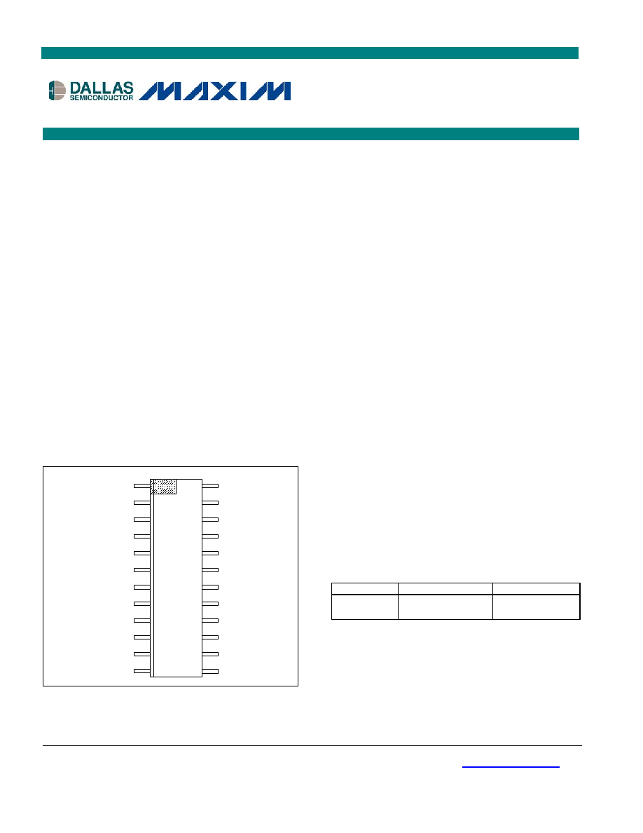
PIN CONFIGURATION
TEST_CG
VBAT
PUMP_ONZ
TEST_RX
NC
NC
NC
NC
TEST_SPLY
NC
GND
I/O
VPAD
SCLK
SDATA
CNVST
NC
NC
NC
NC
AGND
X1
ALARM
X2
1
2
3
4
5
6
7
8
9
10
11
12
24
23
22
21
20
19
18
17
16
15
14
13
FEATURES
ß Automatically Wakes Up, Measures Temperature
and/or Reads an External ADC and Stores
Values in 8kB of Datalog Memory in 8 or 16-Bit
Format
ß On-Chip Direct-to-Digital Temperature Converter
with 8-Bit (0.5∞C) or 11-Bit (0.0625∞C) Resolution
ß Sampling Rate from 1s up to 273hrs
ß Programmable Recording Start Delay After
Elapsed Time or Upon a Temperature Alarm Trip
Point
ß Programmable High and Low Trip Points for
Temperature and Data Alarms
ß Quick Access to Alarmed Devices Through
1-Wire Conditional Search Function
ß 512 Bytes of General-Purpose Memory Plus 64
Bytes of Calibration Memory
ß Two-Level Password Protection of all Memory
and Configuration Registers
ß Unique Factory-Lasered 64-Bit Registration
Number Assures Error-Free Device Selection
and Absolute Part Identity
ß Built-in Multidrop Controller Ensures Com-
patibility with Other Dallas Semiconductor 1-Wire
Net Products
ß Directly Connects to a Single Port Pin of a Mi-
croprocessor and Communicates at Up to
15.4kbps at Standard Speed or up to 125kbps in
Overdrive Mode
ß -40∞C to +85∞C Operating Range
ß 2.8V to 3.6V Single-Supply Battery Operation
ß Low Power (1.2µA Standby, 350µA Active)
ORDERING INFORMATION
PART
TEMP RANGE
PIN-PACKAGE
DS2422S
-40
∞C to +85∞C
24-lead, 300-mil
SO
Commands, Registers, and Modes are capitalized for
clarity.
DS2422
1-Wire Temperature/Datalogger
with 8kB Datalog Memory
www.maxim-ic.com
TOP VIEW
1-Wire is a registered trademark of Dallas Semiconductor.
DS2422
2 of 48
ABSOLUTE MAXIMUM RATINGS*
ALARM, PUMP_ONZ, SDATA, SCLK, CNVST, VPAD,
I/O Voltage to GND
-0.3V, +6V
ALARM, PUMP_ONZ, I/O Combined Sink Current
20mA
Operating Temperature Range
-40∞C to +85∞C
Junction Temperature
+150∞C
Storage Temperature Range
-55∞C to +125∞C
Soldering Temperature
See IPC/JEDEC J-STD-020A
Stresses beyond those listed under "Absolute Maximum Ratings" may cause permanent damage to the device. These are stress ratings only,
and functional operation of the device at these or any other conditions beyond those indicated in the operational sections of the specifications is
not implied. Exposure to the absolute maximum rating conditions for extended periods may affect device.
ELECTRICAL CHARACTERISTICS
(V
PUP
= 3.0V to 5.25V, V
BAT
= 2.0V to 3.6V, V
PAD
= 3.0V to 5.5V, T
A
= -40∞C to +85∞C.
)
PARAMETER
SYMBOL
CONDITIONS
MIN
TYP
MAX
UNITS
I
BAT1
V
BAT
at 3.0V, I/O at 0V, RTC on
1200
2000
Standby Supply Current
I
BAT0
V
BAT
at 3.6V, I/O at 0V, RTC off
50
650
nA
Ground Current
I
GND
Applies individually to GND, AGND
(Note 1)
20
mA
I/O Pin General Data
1-Wire Pullup Resistance
R
PUP
(Notes 1, 2)
2.2
k
W
Input Capacitance
C
IO
(Notes 3, 4)
100
800
pF
Input Load Current
I
L
I/O pin at V
PUP,
V
BAT
= 3.6V
6
10
µA
High-to-Low Switching
Threshold
V
TL
(Notes 4, 5, 6)
0.4
3.2
V
Input Low Voltage
V
IL
(Notes 1, 7)
0.3
V
Low-to-High Switching
Threshold
V
TH
(Notes 4, 5, 8)
0.7
3.4
V
Switching Hysteresis
V
HY
(Notes 4, 9)
0.09
N/A
V
Output Low Voltage
V
OL
At 4mA (Note 10)
0.4
V
Standard speed, R
PUP
= 2.2k
W
5
Overdrive speed, R
PUP
= 2.2k
W
2
Recovery Time (Note 1)
t
REC
Overdrive speed, directly prior to reset
pulse; R
PUP
= 2.2k
W
5
µs
Rising-Edge Hold-off Time
t
REH
(Notes 4, 11)
0.6
2.0
µs
Standard speed
65
Overdrive speed, V
PUP
> 4.5V
8
Timeslot Duration (Note 1)
t
SLOT
Overdrive speed (Note 12)
9.5
µs
I/O Pin, 1-Wire Reset, Presence Detect Cycle
Standard speed, V
PUP
> 4.5V
480
720
Standard speed (Note 12)
690
720
Overdrive speed, V
PUP
> 4.5V
48
80
Reset Low Time (Note 1)
t
RSTL
Overdrive speed (Note 12)
70
80
µs
Standard speed, V
PUP
> 4.5V
15
60
Standard speed (Note 12)
15
63.5
Presence Detect High
Time
t
PDH
Overdrive speed (Note 12)
2
7
µs
Standard speed, V
PUP
> 4.5V
1.5
5
Standard speed
1.5
8
Presence Detect Fall Time
(Notes 4, 13)
t
FPD
Overdrive speed
0.15
1
µs
Standard speed, V
PUP
> 4.5V
60
240
Standard speed (Note 12)
60
287
Overdrive speed, V
PUP
> 4.5V
(Note 12)
7
24
Presence Detect Low
Time
t
PDL
Overdrive speed (Note 12)
7
28
µs
Standard speed, V
PUP
> 4.5V
65
75
Standard speed
71.5
75
Presence Detect Sample
Time (Note 1)
t
MSP
Overdrive speed
8
9
µs

DS2422
3 of 48
PARAMETER
SYMBOL
CONDITIONS
MIN
TYP
MAX
UNITS
I/O Pin, 1-Wire Write
Standard speed
60
120
Overdrive speed, V
PUP
> 4.5V
(Note 12)
6
12
Write-0 Low Time (Note 1)
t
W0L
Overdrive speed (Note 12)
7.5
12
µs
Standard speed
5
15 -
e
Write-1 Low Time
(Notes 1, 14)
t
W1L
Overdrive speed
1
1.95 -
e
µs
I/O Pin, 1-Wire Read
Standard speed
5
15 -
d
Read Low Time
(Notes 1, 15)
t
RL
Overdrive speed
1
1.95 -
d
µs
Standard speed
t
RL
+
d
15
Read Sample Time
(Notes 1, 15)
t
MSR
Overdrive speed
t
RL
+
d
1.95
µs
ALARM Output Pin
Output Low Voltage
V
OL
Sink current 4mA
0.6
V
Pin Leakage Current
I
LP
ALARM pin at 6V
6
µA
CNVST, SCLK Output Pins
V
PAD
= 5V, I
L
= 3mA
0.3
Output Low Voltage
V
OL
V
PAD
= 3V, I
L
= 3mA
0.3
V
V
PAD
= 5V, I
L
= 3mA
4
Output High Voltage
V
OH
V
PAD
= 3V, I
L
= 3mA
2
V
PUMP_ONZ Output Pin
V
BAT
= 3.6V, I
L
= 2mA
0.4
Output Low Voltage
V
OL
V
BAT
= 2.0V, I
L
= 2mA
0.4
V
Output High Voltage
V
BAT
= 3.6V, I
L
= 0.5mA
2.5
V
OH
V
BAT
= 2.0V, I
L
= 0.5mA
1.4
V
SDATA Input Pin
V
BAT
= 3.6V
2.5
Input High Voltage
V
IH
V
BAT
= 2.0V
1.4
V
V
BAT
= 3.6V
0.4
Input Low Voltage
V
IL
V
BAT
= 2.0V
0.4
V
Pin Leakage Current
I
LP
SDATA pin at 5.5V
10
µA
Serial Interface Timing
CLK Period
t
RING
0.5
1
9
µs
PUMP_ONZ Fall to
CNVST Rise
t
SP
Power-on default (Notes 4, 19)
3.5
4
4.5
ms
CNVST Pulse Width
t
CPW
(Note 4)
70
140
1260
µs
CNVST Fall to SCLK High
(First Clock)
t
SCH
(Note 4)
8
16
144
µs
SCLK Period
t
SCP
50% duty cycle (Note 4)
1
2
18
µs
SDATA Setup Time
t
SDS
(Note 4)
75
ns
SDATA Hold Time
t
SDH
(Note 4)
3
ns
Real-Time Clock
Accuracy
+25∞C (Note 16)
-2
+2
min./
month
Frequency Deviation
D
F
-40∞C to +85∞C (Note 16)
-300
+60
PPM
Temperature Converter
Operating Range
T
TC
3V at V
BAT
-40
+85
∞C
8-bit mode
30
50
75
Conversion Time (Note 4)
t
CONV
16-bit mode (11 bits)
240
400
600
ms
Thermal Response Time
Constant (Notes 4, 17)
t
RESP
SO package
95
s
+10∞C to +60∞C
Conversion Error
(Notes 4, 18)
DJ
-40∞C to +85∞C
See Temperature Accuracy
Graphs
∞C
Conversion Current
I
CONV
(Note 4)
180
350
550
µA
DS2422
4 of 48
Note 1:
System Requirement
Note 2:
Maximum allowable pullup resistance is a function of the number of 1-Wire devices in the system and 1-Wire recovery times. The
specified value here applies to systems with only one device and with the minimum 1-Wire recovery times. For more heavily
loaded systems, an active pullup such as that found in the DS2480B may be required.
Note 3:
Capacitance on the data pin could be 800pF when V
PUP
is first applied. If a 2.2k
W resistor is used to pull up the data line, 2.5µs
after V
PUP
has been applied the parasite capacitance will not affect normal communications.
Note 4:
Guaranteed by design, not production tested.
Note 5:
V
TL
, V
TH
are a function of the internal supply voltage.
Note 6:
Voltage below which, during a falling edge on I/O, a logic '0' is detected.
Note 7:
The voltage on I/O needs to be less or equal to V
ILMAX
whenever the master drives the line low.
Note 8:
Voltage above which, during a rising edge on I/O, a logic '1' is detected.
Note 9:
After V
TH
is crossed during a rising edge on I/O, the voltage on I/O has to drop by V
HY
to be detected as logic '0'.
Note 10:
The I-V characteristic is linear for voltages less than 1V.
Note 11:
The earliest recognition of a negative edge is possible at t
REH
after V
TH
has been previously reached.
Note 12:
Highlighted numbers are NOT in compliance with the published iButton standards. See comparison table below.
Note 13:
Interval during the negative edge on I/O at the beginning of a Presence Detect pulse between the time at which the voltage is
90% of V
PUP
and the time at which the voltage is 10% of V
PUP
.
Note 14:
e represents the time required for the pullup circuitry to pull the voltage on I/O up from V
IL
to V
TH
.
Note 15:
d represents the time required for the pullup circuitry to pull the voltage on I/O up from V
IL
to the input high threshold of the bus
master.
Note 16:
This is the expected range when using a crystal equivalent to the KDS SN14J (12.5pF).
Note 17:
Time to reach 63% of the temperature change; measured at a temperature transition step from +25∞C to +85∞C.
Note 18:
A 2-point calibration trim at 3V must be done to achieve the specified accuracy at 3V. An application note is available to help
developers perform the calibration by writing the trim registers to properly orient the error curve.
Note 19:
The duration is user-programmable from 0ms (code 00h) to 127.5ms (code FFh) with a tolerance of ±0.5ms. See Delay Register,
address 400h, for details.
STANDARD VALUES
DS2422 VALUES
PARAMETER
STANDARD SPEED
OVERDRIVE SPEED
STANDARD SPEED
OVERDRIVE SPEED
NAME
MIN
MAX
MIN
MAX
MIN
MAX
MIN
MAX
t
SLOT
(incl. t
REC
)
61µs
(undef.)
7µs
(undef.)
65µs
1)
(undef.)
9.5µs
(undef.)
t
RSTL
480µs
(undef.)
48µs
80µs
690µs
720µs
70µs
80µs
t
PDH
15µs
60µs
2µs
6µs
15µs
63.5µs
2µs
7µs
t
PDL
60µs
240µs
8µs
24µs
60µs
287µs
7µs
28µs
t
W0L
60µs
120µs
6µs
16µs
60µs
120µs
7.5µs
12µs
1)
Intentional change, longer recovery time requirement due to modified 1-Wire front end.
DS2422
5 of 48
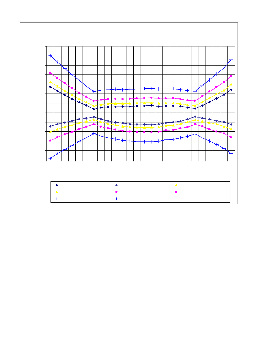
DS2422 Temperature Accuracy at 3V
-2.500
-2.000
-1.500
-1.000
-0.500
0.000
0.500
1.000
1.500
2.000
2.500
3.000
3.500
-40
-30
-20
-10
0
10
20
30
40
50
60
70
80
Temperature (∞C)
E
r
ro
r (
∞
C
)
Max. ± 0.1∞C uncertainty
Min. ± 0.1∞C uncertainty
Max. ±0.25∞C uncertainty
Min. ±0.25∞C uncertainty
Max. ±0.5∞C uncertainty
Min. ±0.5∞C uncertainty
Max. ±1∞C uncertainty
Min. ±1∞C uncertainty
"Uncertainty" refers to the uncertainty of the temperature measurement when performing the 2-point calibration trim
as described in the application note. These graphs assume 11-bit temperature conversion. The accuracy can be
improved further through software correction. See the application note referenced as "Note 18" on the previous
page for details.

DS2422
6 of 48
PIN DESCRIPTION
PIN
NAME
FUNCTION
1
VPAD
Operating voltage of the serial interface pads CNVST, SCLK, SDATA. Used for
level translation from the VBAT-powered internal logic to the 5V-powered ADC.
Connect to VBAT if the serial interface is not used.
2
SCLK
Serial clock signal for serial interface. May connect directly to the corresponding
MAX1086 pin. The idle state for the pin is low.
3
SDATA
Serial data pin for the serial interface. May connect directly to the DOUT pin of
MAX1086. The pin includes a weak pulldown and therefore has an idle state of low.
4
CNVST
Conversion Start control signal for the MAX1086. The idle state for the pin is low.
9
AGND
Analog ground. Ground reference for external ADC and charge pump.
10
X1
First of two crystal pins for the real time clock crystal. A standard 6pF 32KHz crystal
is used. The accuracy of the device's real time clock is largely dependent on the
temperature characteristics of the crystal. Trace length from the device to the crystal
should be minimized to reduce their capacitive effect.
11
ALARM
Logic open-drain output with 215
W maximum on-resistance, operating range 0V to
5.25V. Power-on default is OFF.
12
X2
Second of two crystal pins for the real time clock crystal.
13
IO
1-Wire communication line, data input and output. This pin also charges the internal
parasitic power cap that allows the 1-Wire front end of the device to run without
VBAT supply.
14
GND
Common ground supply for the device and VBAT.
16
TEST_SPLY
Connect to GND (test pin)
21
TEST_RX
Connect to GND (test pin)
22
PUMP_ONZ
Signal to control an external charge-pump. The signal polarity is designed to fit to
the MAX619 charge pump/regulator.
23
VBAT
3V power supply for the device, typically a battery. This pin supplies power to all
parts of the device except for the 1-Wire front end.
24
TEST_CG
Do not connect (test pin)
9 pins
NC
Not connected
DESCRIPTION
The DS2422 temperature/data logger combines the core functions of a fully featured data logger in a single chip. It
includes a temperature sensor, RTC, memory, 1-Wire interface, and serial interface for an analog-to-digital
converter (ADC) as well as control circuitry for a charge pump. The ADC and the charge pump are peripherals that
can be added to build application-specific data loggers. Without external ADC, the DS2422 functions as a
temperature logger only. The DS2422 measures the temperature and/or reads the ADC at a user-defined rate. A
total of 8192 8-bit readings or 4096 16-bit readings taken at equidistant intervals ranging from 1 second to 273
hours can be stored. In addition to this, there are 512 bytes of SRAM for storing application specific information and
64 bytes for calibration data. A mission to collect data can be programmed to begin immediately, after a user-
defined delay, or after a temperature alarm. Access to the memory and control functions can be password-
protected. The DS2422 is configured and communicates with a host computing device through the serial 1-Wire
protocol, which requires only a single data lead and a ground return. Every DS2422 is factory-lasered with a
guaranteed unique 64-bit registration number that allows for absolute traceability. The extremely low energy con-
sumption in conjunction with its high level of programmability makes the DS2422 the ideal choice for low-cost data
loggers that can take millions of measurements from the energy of a single 3V button cell.
APPLICATION
The DS2422 allows the design of data loggers or monitors with a minimum number of components. The simple
circuit of Figure 1 can monitor body or room temperature with 0.0625∞C resolution. For very high temperature-
monitoring applications, a thermocouple can be connected to the analog-to-digital converter (ADC) through a pre-
amplifier, as shown in Figure 2. The internal temperature sensor of the DS2422 keeps track of the reference
temperature, which is needed to accurately convert the voltage reading of the thermocouple into the actual
temperature of the monitored object. A less obvious application of the DS2422 is inside of major equipment.
Besides the temperature inside the chassis, the serial interface can monitor up to 16 digital signals, which are
parallel-clocked into an external shift register by CNVST and then shifted into the DS2422 through the SDATA pin
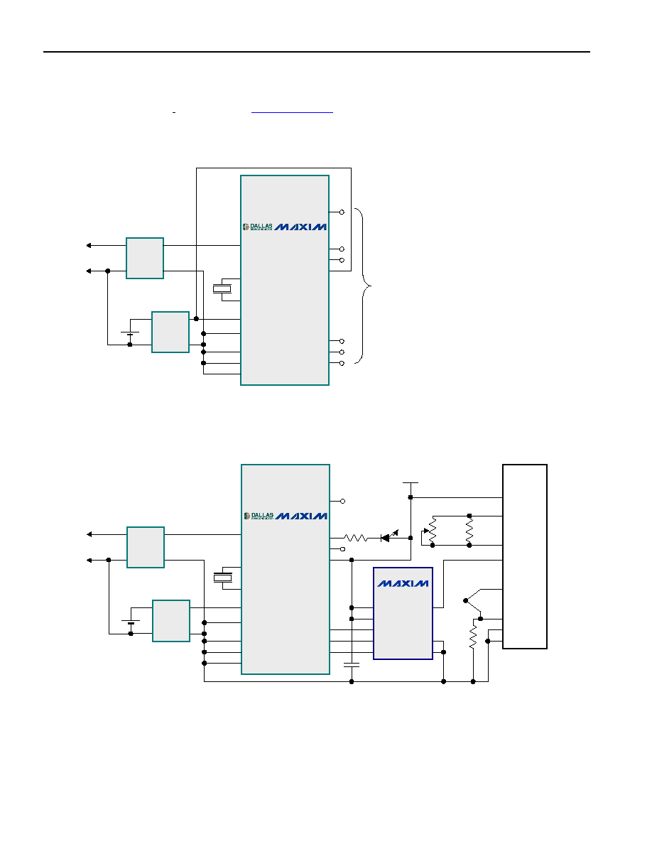
DS2422
7 of 48
under the control of SCLK. The DS2422 will activate its alarm output if the measured temperature or serial-input
data reaches a user-programmed high or low alarm threshold. This alarm then can be used to shut down the
equipment and enforce a service call. In contrast to microprocessor-based data loggers, the DS2422 does not
require any firmware development. Software for setup and data retrieval through the 1-Wire interface is available
for free download from the iButton website (
www.ibutton.com
). This software also includes drivers for the serial and
USB port 1-Wire interfaces of a PC, and routines to access the general-purpose memory for storing application or
equipment-specific data files.
Figure 1. Simple Temperature Logger
KDS
SM14J
32768Hz
1-Wire
GND
Leave
open
BR1225R
Lithium
1
2
6
5
IC2
DS9503
1
2
6
5
IC3
DS9503
SDATA
SCLK
CNVST
AGND
GND
VBAT
VPAD
X2
IO
PUMP_ONZ
ALARM
CLK_TEST
TEST_EXT
OSC_TEST
X1
IC1
DS2422
SDATA
SCLK
CNVST
AGND
GND
VBAT
VPAD
X2
IO
PUMP_ONZ
ALARM
X1
TEST_SPLY
TEST_RX
TEST_CG
Figure 2. Temperature and Voltage Logger With Thermocouple
D1
1.5V LED
C1
0.1
mF
5V
1-Wire
GND
Leave
open
BR1225R
Lithium
KDS
SM14J
32768Hz
Thermocouple
Type E, J, K, N
R1
470
W
R3
2k
R4
2.2k
W
R2
200k
7
8
1
6
3
2
5
4
IC3
INA122
V-
Ref
Vin-
Vin+
Vo
RG
RG
V+
1
2
6
5
IC4
DS9503
1
2
6
5
IC5
DS9503
IC2
MAX1086
DOUT
SCLK
CNVST
REF
VDD
GND
AIN2
AIN1
1
5
6
8
7
2
3
4
SDATA
SCLK
CNVST
AGND
GND
VBAT
VPAD
X2
IO
PUMP_ONZ
ALARM
CLK_TEST
TEST_EXT
OSC_TEST
X1
IC1
DS2422
SDATA
SCLK
CNVST
AGND
GND
VBAT
VPAD
X2
IO
PUMP_ONZ
ALARM
TEST_CG
X1
TEST_SPLY
TEST_RX
Note: When using a positive/negative thermocouple, an offset voltage can be utilized through the Ref input of the
INA122 amplifier. This voltage shifts the 0V output of the amplifier up the amount equal to the offset voltage
allowing negative voltages to be read in the positive range of the MAX1086. This offset voltage may be obtained
through a simple resistor divider network (not shown).

DS2422
8 of 48
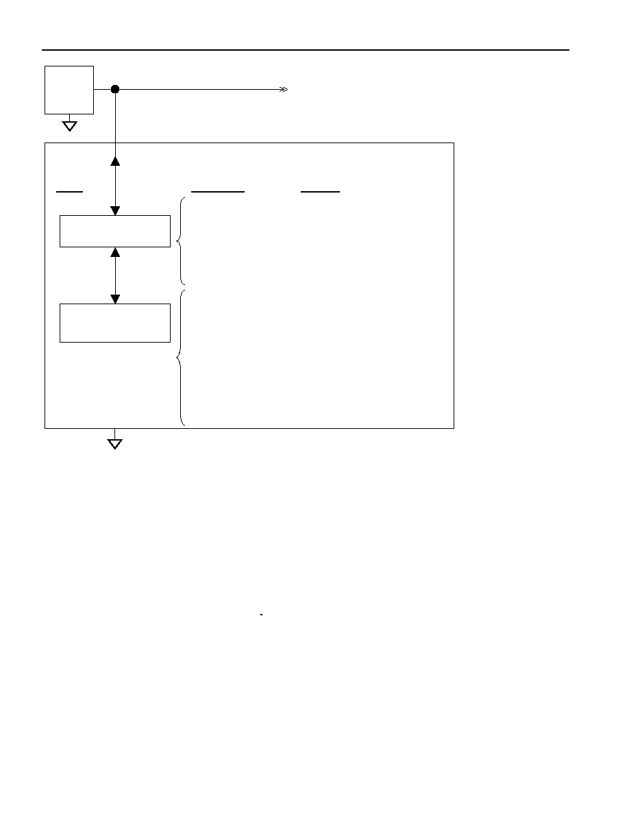
Figure 3. DS2422 Block Diagram
All circuitry is powered by the battery
unless otherwise specified
Internal
Timekeeping &
Control Reg. &
Counters
3V Lithium
General-Purpose
SRAM
(512 Bytes)
Register Pages
(64 Bytes)
Calibration Memory
(64 Bytes)
Datalog
Memory
8k Bytes
32.768kHz
Oscillator
Control
Logic
256-Bit
Scratchpad
Memory
Function
Control
ROM
Function
Control
64-Bit
Lasered
ROM
Parasite
Powered
Circuitry
1-Wire
Port
I/O
ADC1
Thermal
Sense
VPAD
CNVST
SCLK
SDATA
PUMP_ONZ
5V Pad
Structures
Powered by VBAT
OVERVIEW
The block diagram in Figure 3 shows the relationships between the major control and memory sections of the
DS2422. The device has six main data components: 1) 64-bit lasered ROM, 2) 256-bit scratchpad, 3) 512-byte
general-purpose SRAM, 4) two 256-bit register pages of timekeeping, control, status, and counter registers and
passwords, 5) 64 bytes of calibration memory, and 6) 8192 bytes of data-logging memory. Except for the ROM and
the scratchpad, all other memory is arranged in a single linear address space. The data-logging memory, counter
registers and several other registers are read-only for the user. Both register pages are write-protected while the
device is programmed for a mission. The password registers, one for a read password and another one for a
read/write password can only be written to, never read.
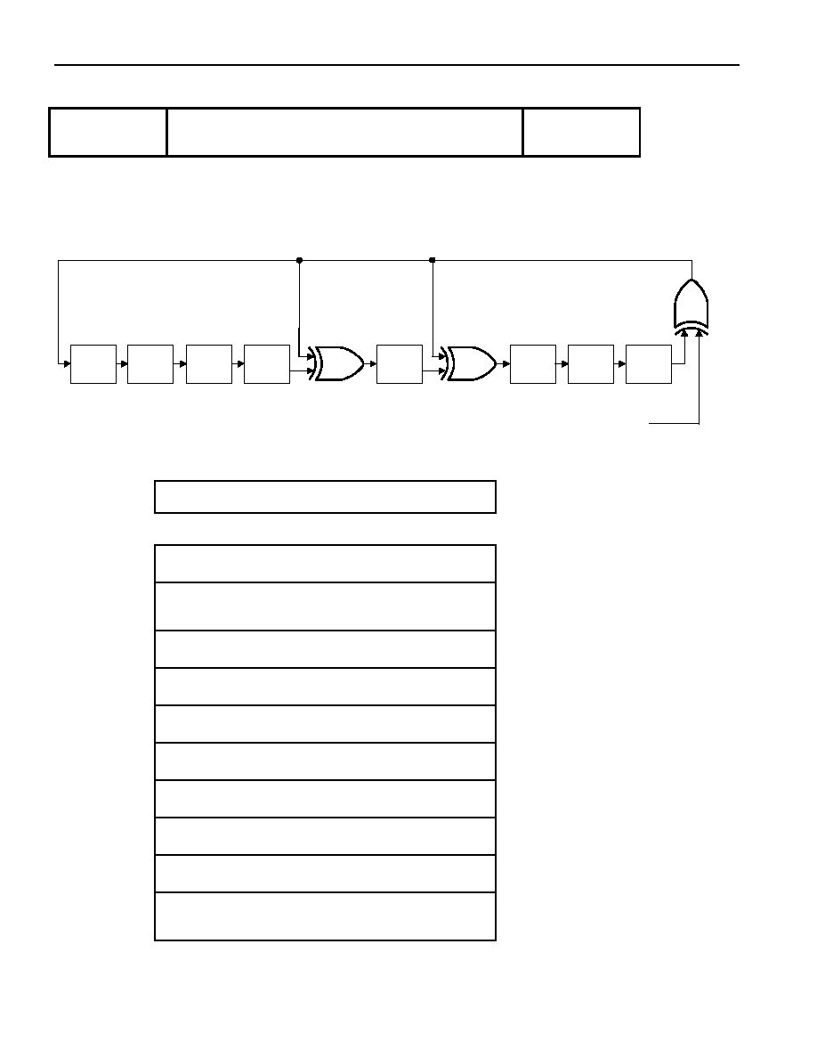
The hierarchical structure of the 1-Wire protocol is shown in Figure 4. The bus master must first provide one of the
eight ROM function commands: 1) Read ROM, 2) Match ROM, 3) Search ROM, 4) Conditional Search ROM, 5)
Skip ROM, 6) Overdrive-Skip ROM, 7) Overdrive-Match ROM or 8) Resume. Upon completion of an Overdrive
ROM command byte executed at standard speed, the device will enter Overdrive mode, where all subsequent
communication occurs at a higher speed. The protocol required for these ROM function commands is described in
Figure 14. After a ROM function command is successfully executed, the memory and control functions become
accessible and the master may provide any one of the eight available commands. The protocol for these memory
and control function commands is described in Figure 12. All data is read and written least significant bit first.
DS2422
9 of 48
Figure 4. Hierarchical Structure for 1-Wire Protocol
1-Wire net
Other
Devices
BUS
Master
DS2422
Available
Commands:
Command
Level:
Data Field
Affected:
1-Wire ROM Function
Commands
DS2422-specific
Memory Function
Commands
Read ROM
Match ROM
Search ROM
Conditional Search ROM
Skip ROM
Resume
Overdrive Skip
Overdrive Match
64-bit ROM, RC-Flag
64-bit ROM, RC-Flag
64-bit ROM, RC-Flag
64-bit ROM, RC-Flag, Alarm Flags,
Search Conditions
RC-Flag
RC-Flag
RC-Flag, OD-Flag
64-bit ROM, RC-Flag, OD-Flag
Write Scratchpad
Read Scratchpad
Copy Scratchpad w/PW
Read Memory w/PW
Read Memory w/PW &
w/CRC
Clear Memory w/PW
Forced Conversion
Start Mission w/PW
Stop Mission w/PW
256-bit Scratchpad, Flags
256-bit Scratchpad
512 byte Data Memory, Registers,
Flags, Passwords
Memory, Registers, Passwords
Memory, Registers, Passwords
Mission Time Stamp, Mission Samples
Counter, Start Delay, Sample
Rate Register, Alarm Flags,
Passwords
Memory addresses 020C to 020Fh
Flags, Timestamp
Flags
PARASITE POWER
The block diagram (Figure 3) shows the parasite-powered circuitry. This circuitry "steals" power whenever the I/O
input is high. I/O provides sufficient power as long as the specified timing and voltage requirements are met. The
advantages of parasite power are two-fold: 1) by parasiting off this input, battery power is conserved; and 2) if the
battery is exhausted for any reason, the ROM may still be read.
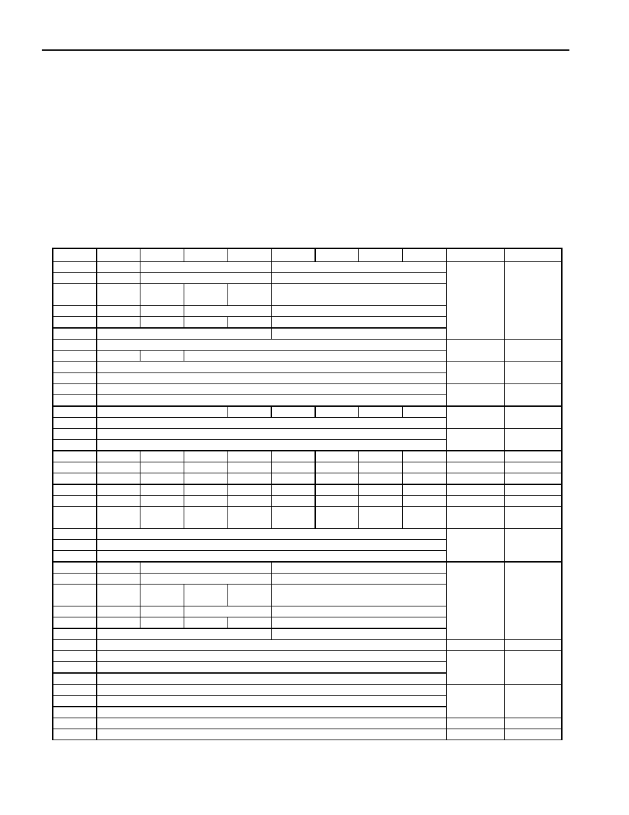
64-BIT LASERED ROM
Each DS2422 contains a unique ROM code that is 64 bits long. The first 8 bits are a 1-Wire family code. The next
48 bits are a unique serial number. The last 8 bits are a CRC of the first 56 bits. See Figure 5 for details. The
1-Wire CRC is generated using a polynomial generator consisting of a shift register and XOR gates as shown in
Figure 6. The polynomial is X
8
+ X
5
+ X
4
+ 1. Additional information about the Dallas 1-Wire CRC is available in
Application Note 27 and in the Book of DS19xx iButton Standards.
The shift register bits are initialized to 0. Then starting with the least significant bit of the family code, one bit at a
time is shifted in. After the 8
th
bit of the family code has been entered, then the serial number followed by the
temperature range code is entered. After the range code has been entered, the shift register contains the CRC
value. Shifting in the 8 bits of CRC returns the shift register to all 0s.
DS2422
10 of 48
Figure 5. 64-Bit Lasered ROM
MSB
LSB
8-Bit
CRC Code
48-Bit Serial Number
8-Bit Family
Code (41h)
MSB
LSB
MSB
LSB
MSB LSB
Figure 6. 1-Wire CRC Generator
X
0
X
1
X
2
X
3
X
4
X
5
X
6
X
7
X
8
Polynomial = X
8
+ X
5
+ X
4
+ 1
1
st
STAGE
2
nd
STAGE
3
rd
STAGE
4
th
STAGE
6
th
STAGE
5
th
STAGE
7
th
STAGE
8
th
STAGE
INPUT DATA
Figure 7. DS2422 Memory Map
32-Byte Intermediate Storage Scratchpad
ADDRESS
0000H to
001FH
32-Byte General-Purpose SRAM (R/W)
Page 0
0020H to
01FFH
General-Purpose SRAM (R/W)
Pages 1
to 15
0200H to
021FH
32-Byte Register Page 1
Page 16
0220H to
023FH
32-Byte Register Page 2
Page 17
0240H to
025FH
Calibration Memory Page 1 (R/W)
Page 18
0260H to
027FH
Calibration Memory Page 2 (R/W)
Page 19
0280H to
03FFH
(Reserved For Future Extensions)
Pages 20 to 31
0400H to
041FH
Trim Register Page (R/W)
Page 32
0420H to
0FFFH
(Reserved For Future Extensions)
Pages 33 to 127
1000H to
2FFFH
Datalog Memory (Read-Only)
Pages 128
to 383
DS2422
11 of 48
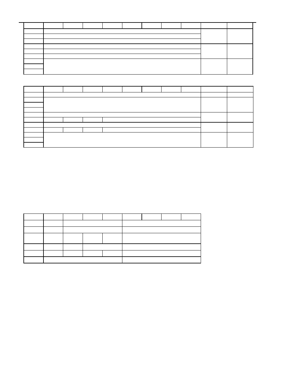
MEMORY
The memory map of the DS2422 is shown in Figure 7. The 512 bytes general-purpose SRAM are located in pages
0 through 15. The various registers to set up and control the device fill page 16 and 17, called Register Pages 1
and 2 (details in Figure 8). Pages 18 and 19 provide storage space for calibration data. They can alternatively be
used as extension of the general-purpose memory. The Trim Register Page holds registers that are used to tune
the timing of the serial data interface and to trim the on-chip temperature converter. The "datalog" logging memory
starts at address 1000h (page 128) and extends over 256 pages. The memory pages 20 to 31 and 33 to 127
are
reserved for future extensions. The scratchpad is an additional page that acts as a buffer when writing to the SRAM
memory or the register page. The data- and calibration memory can be written at any time. The access type for the
two register pages and the Trim Register Page is register-specific and depends on whether the device is pro-
grammed for a mission. Figures 8A and 8B show
the details. The datalog memory is read-only for the user. It is
written solely under supervision of the on-chip control logic. Due to the special behavior of the write access logic
(write scratchpad, copy scratchpad) it is recommended to only write full pages at a time. This also applies to all the
register pages and the calibration memory. See section Address Register and Transfer Status for details.
Figure 8A. DS2422 Register Pages Map
ADDR
b7
b6
b5
b4
b3
b2
b1
b0
Function
Access*
0200h
0
10 Seconds
Single Seconds
0201h
0
10 Minutes
Single Minutes
Real-
0202h
0
12/24
20h.
AM/PM
10h.
Single Hours
Time Clock
R/W; R
0203h
0
0
10 Date
Single Date
Registers
0204h
CENT
0
0
10m.
Single Months
0205h
10 Years
Single Years
0206h
Low Byte
Sample
0207h
0
0
High Byte
Rate
R/W; R
0208h
Low Threshold
Temp.
0209h
High Threshold
Alarms
R/W; R
020Ah
Low Threshold
020Bh
High Threshold
Data
Alarms
R/W; R
020Ch
Low Byte
0
0
0
0
0
Latest
R; R
020Dh
High Byte
Temp.
020Eh
Low Byte
020Fh
High Byte
Latest
Data
R; R
0210h
0
0
0
0
0
0
ETHA
ETLA
T.Alm.En.
R/W; R
0211h
1
1
1
1
1
1
EDHA
EDLA
D.Alm.En.
R/W; R
0212h
0
0
0
0
0
0
EHSS
EOSC
RTC En.
R/W; R
0213h
1
1
SUTA
RO
DLFS
TLFS
EDL
ETL
Mis. Cntrl.
R/W; R
0214h
BOR
1
1
1
DHF
DLF
THF
TLF
Alm. Stat.
R; R
0215h
1
1
0
WFTA
MEMC
LR
0
MIP
0
Gen. Stat.
R; R
0216h
Low Byte
Start
0217h
Center Byte
Delay
R/W; R
0218h
High Byte
Counter
0219h
0
10 Seconds
Single Seconds
021Ah
0
10 Minutes
Single Minutes
021Bh
0
12/24
20h.
AM/PM
10h.
Single Hours
Mission
Time
R; R
021Ch
0
0
10 Date
Single Date
Stamp
021Dh
CENT
0
0
10m.
Single Months
021Eh
10 Years
Single Years
021Fh
(no function; reads 00h)
(N/A)
R; R
0220h
Low Byte
Mission
0221h
Center Byte
Samples
R; R
0222h
High Byte
Counter
0223h
Low Byte
Device
0224h
Center Byte
Samples
R; R
0225h
High Byte
Counter
0226h
Configuration Code
Flavor
R; R
0227h
EPW
PW. Cntrl.
R/W; R
DS2422
12 of 48
ADDR
b7
b6
b5
b4
b3
b2
b1
b0
Function
Access*
0228h
First Byte
Read
--
--
Access
W; --
022Fh
Eighth Byte
Password
0230h
First Byte
Full
--
--
Access
W; --
0237h
Eighth Byte
Password
0238h
--
(no function; all of these bytes read 00h)
(N/A)
R; R
023Fh
Figure 8B. DS2422 Trim Register Page Map
ADDR
b7
b6
b5
b4
b3
b2
b1
b0
Function
Access*
0400h
delay value
t
SP
R/W; R
0401h
--
(no function; undefined read)
(N/A)
R; R
0403h
0404h
Temperature Counter Reset Low Byte
0405h
0
0
0
Temperature Counter Reset High Byte
R/W; R/W
0406h
Temperature Conversion Length Low Byte
0407h
0
0
0
Temperature Conversion Length High Byte
R/W; R/W
0408h
--
(no function; undefined read)
(N/A)
R; R
041Fh
Note: The first entry in column ACCESS TYPE is valid between missions. The second entry shows the applicable
access type while a mission is in progress.
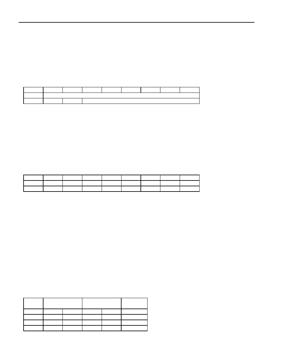
TIMEKEEPING AND CALENDAR
The RTC/alarm and calendar information is accessed by reading/writing the appropriate bytes in the register page,
address 200h to 205h. For readings to be valid, all RTC registers must be read sequentially starting at address
0200h. Some of the RTC bits are set to 0. These bits always read 0 regardless of how they are written. The
number representation of the RTC registers is BCD format (binary-coded decimal).
Real-Time Clock and RTC Alarm Register Bitmap
ADDR
b7
b6
b5
b4
b3
b2
b1
b0
0200h
0
10s
Single Seconds
0201h
0
10 min.
Single Minutes
0202h
0
12/24
20hr
AM/PM
10hr
Single Hours
0203h
0
0
10 Date
Single Date
0204h
CENT
0
0
10m.
Single Months
0205h
10yrs
Single Years
The RTC of the DS2422 can run in either 12-hour or 24-hour mode. Bit 6 of the Hours Register (address 202h) is
defined as the 12- or 24-hour mode select bit. When high, the 12-hour mode is selected. In the 12-hour mode, bit 5
is the AM/PM bit with logic 1 being PM. In the 24-hour mode, bit 5 is the 20-hour bit (20 to 23 hours). The CENT bit,
bit 7 of the Months Register, can be written by the user. This bit changes its state when the years counter
transitions from 99 to 00.
The calendar logic is designed to automatically compensate for leap years. For every year value that is either 00 or
a multiple of 4 the device adds a 29
th
of February. This works correctly up to (but not including) the year 2100.
DS2422
13 of 48
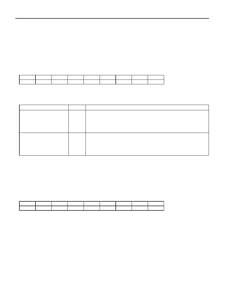
SAMPLE RATE
The content of the Sample Rate Register (addresses 0206h, 0207h) specifies the time elapse (in seconds if EHSS
= 1, or minutes if EHSS = 0) between two temperature/data logging events. The sample rate may be any value
from 1 to 16383, coded as an unsigned 14-bit binary number. If EHSS = 1, the shortest time between logging
events is 1 second and the longest (sample rate = 3FFFh) is 4.55 hours. If EHSS = 0, the shortest is 1 minute and
the longest time is 273.05 hours (sample rate = 3FFFh). The EHSS bit is located in the RTC Control Register at
address 0212h. It is important that the user sets the EHSS bit accordingly while setting the Sample Rate register. A
sample rate of 0000h is not valid and must be avoided under all circumstances. This causes the device to enter
into an undefined state, requiring a power-on reset and restore of the trim settings to recover.
Sample Rate Register Bitmap
ADDR
b7
b6
b5
b4
b3
b2
b1
b0
0206h
Sample Rate Low
0207h
0
0
Sample Rate High
During a mission, there is only read access to these registers. Bits cells marked "0" always read 0 and cannot be
written to 1.
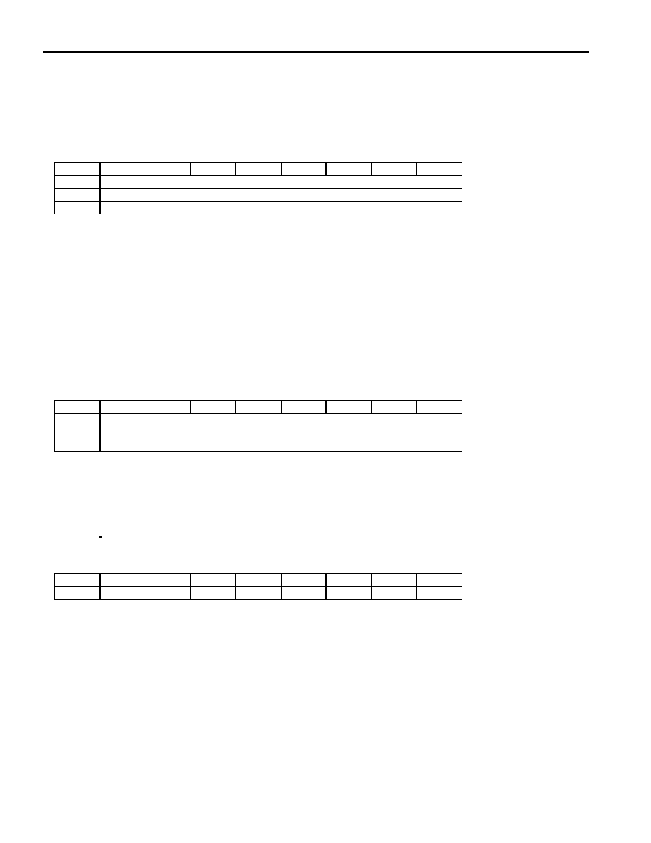
TEMPERATURE CONVERSION
The DS2422 can measure temperatures from -40∞C to +85∞C. Temperature values are represented as an 8- or 16-
bit unsigned binary number with a resolution of 0.5∞C in the 8-bit mode and 0.0625∞C in the 16-bit mode.
The higher temperature byte TRH is always valid. In the 16-bit mode only the three highest bits of the lower byte
TRL are valid. The five lower bits all read zero. TRL is undefined if the device is in 8-bit temperature mode. An out-
of-range temperature reading is indicated as 00h or 0000h when too cold and FFh or FFE0h when too hot.
Latest Temperature Conversion Result Register Bitmap
ADDR
b7
b6
b5
b4
b3
b2
b1
b0
020Ch
T2
T1
T0
0
0
0
0
0
TRL
020Dh
T10
T9
T8
T7
T6
T5
T4
T3
TRH
With TRH and TRL representing the decimal equivalent of a temperature reading the temperature value is
calculated as
J(∞C) = TRH/2 - 41 + TRL/512
(16 bit mode, TLFS = 1, see address 0213h)
J(∞C) = TRH/2 - 41
(8 bit mode, TLFS = 0, see address 0213h)
This equation is valid for converting temperature readings stored in the datalog memory as well as for data read
from the Latest Temperature Conversion Result Register.
To specify the temperature alarm thresholds, the equation above needs to be resolved to
TALM = 2 *
J (∞C) + 82
Since the temperature alarm threshold is only one byte, the resolution or temperature increment is limited to 0.5∞C.
The TALM value needs to be converted into hexadecimal format before it can be written to one of the temperature
alarm threshold registers (Low Alarm address 0208h; High Alarm address 0209h). Independent of the
conversion mode (8 or 16 bit) only the most significant byte of a temperature conversion is used to determine
whether an alarm will be generated.
Temperature Conversion Examples
Mode
TRH
hex
decimal
TRL
hex
decimal
J(∞C)
8-bit
54h
84
--
--
1.0
8-bit
17h
23
--
--
-29.5
16-bit
54h
84
00h
0
1.000
16-bit
17h
23
60h
96
-29.3125

DS2422
14 of 48
Temperature Alarm Threshold Examples
J(∞C)
TALM
hex
decimal
25.5
85h
133
-10.0
3Eh
62
SERIAL DATA INPUT
In addition to temperature, the DS2422 can log 8-bit or 16-bit digital information that it receives through its serial
interface. This interface is designed to directly connect to ADCs such as the MAX1086 or other circuits that use the
same interface timing. The general timing of the serial interface is shown in Figure 9. All timing is derived from an
on-chip ring oscillator, which generates the CLK signal. The CNVST signal is intended to start an
analog-to-digital
conversion. After the conversion is completed, the SCLK signal becomes active and on its rising edge clocks the
digital value into the DS2422. The PUMP_ONZ signal can activate a MAX619 charge pump to convert the 3V
battery voltage of the DS2422 into 5V, for example, to power additional circuitry.
Figure 9A. Serial Interface Timing
PUMP_ONZ
CNVST
SCLK
SDATA
CLK
B15 B14 B13 B12 b4 B3 B2 B1 B0
t
RING
t
SP
t
CPW
t
SCH
t
SCP
Figure 9B. Serial Interface Setup and Hold Timing
t
SDH
t
SDS
SCLK
SDATA
Data
Valid
The serial interface becomes active whenever the DS2422 executes a Forced Conversion command (see
Memory/Control Function Commands) or during a mission, if the device is set up to log data from its serial
interface. Regardless of its setup, the DS2422 always reads 16 bits from its serial input. The 16-bit result of the
latest serial reading is found at address 020Eh (low byte) and 020Fh (high byte). The first bit read through the
serial interface is always found as B15 at address 020Fh. If an ADC generates less than 16 bits, the internal weak
pulldown of the SDATA pin makes the missing bits read zero.
Latest Serial Data Reading Result Register Bitmap
ADDR
b7
b6
b5
b4
b3
b2
b1
b0
020Eh
B7
B6
B5
B4
B3
B2
B1
B0
LOW
020Fh
B15
B14
B13
B12
B11
B10
B9
B8
HIGH
During a mission, if data logging from the serial input is enabled, the HIGH byte (B15 to B8) is always recorded.
The LOW byte (B7 to B0) is only recorded if the DS2422 is set up for 16-bit logging of serial input data.
The algorithm to convert the digital reading from the serial interface into a physical unit depends on the circuit that
provides the data to the DS2422. This algorithm needs to be reversed when calculating values for the alarm
DS2422
15 of 48
threshold registers that are associated to the serial data input. The registers for data alarm thresholds are
located at address 020Ah (Low Alarm) and 020B (High Alarm). The comparison is based on the most
significant serial input byte and assumes that the data is represented as unsigned binary number.
TEMPERATURE SENSOR ALARM
The DS2422 has two Temperature Alarm Threshold registers (address 0208h, 0209h) to store values, which
determine whether a critical temperature has been reached. A temperature alarm is generated if the device
measures an alarming temperature AND the alarm signaling is enabled. The bits ETLA and ETHA that enable the
temperature alarm are located in the Temperature Sensor Control Register. The temperature alarm flags TLF and
THF are found in the Alarm Status Register at address 0214h.
Temperature Sensor Control Register Bitmap
ADDR
b7
b6
b5
b4
b3
b2
b1
b0
0210h
0
0
0
0
0
0
ETHA
ETLA
During a mission, there is only read access to this register. Bits 2 to 7 have no function. They always read 0 and
cannot be written to 1.
Register Details
BIT DESCRIPTION
BIT(S)
DEFINITION
ETLA: Enable Tempera-
ture Low Alarm
b0
This bit controls whether, during a mission, the Temperature Low
Alarm Flag TLF may be set, if a temperature conversion results in a
value equal to or lower than the value in the Temperature Low Alarm
Threshold Register. If ETLA is 1, temperature low alarms are enabled.
If ETLA is 0, temperature low alarms are not generated.
ETHA: Enable
Temperature High Alarm
b1
This bit controls whether, during a mission, the Temperature High
Alarm Flag THF may be set, if a temperature conversion results in a
value equal to or higher than the value in the Temperature High Alarm
Threshold Register. If ETHA is 1, temperature high alarms are
enabled. If ETHA is 0, temperature high alarms are not generated.
SERIAL INPUT ALARM
The DS2422 has two Data Alarm Threshold registers (address 020Ah, 020Bh) to store values, which determine
whether data read through the serial interface can generate an alarm. Such an alarm is generated if the input data
qualifies for an alarm AND the alarm signaling is enabled. The bits EDLA and EDHA that enable the serial input
alarm are located in the DATA_IF Control Register. The corresponding alarm flags DLF and DHF are found in the
Alarm Status Register at address 0214h.
DATA_IF Control Register Bitmap
ADDR
b7
b6
b5
b4
b3
b2
b1
b0
0211h
1
1
1
1
1
1
EDHA
EDLA
During a mission, there is only read access to this register. Bits 3 to 7 have no function. They always read 1 and
cannot be written to 0.

DS2422
16 of 48
Register Details
BIT DESCRIPTION
BIT(S)
DEFINITION
EDLA: Enable Data Low
Alarm
b0
This bit controls whether, during a mission, the Data Low Alarm Flag
DLF may be set, if a data value from the serial data interface is equal to
or lower than the value in the Data Low Alarm Threshold Register. If
EDLA is 1, data low alarms are enabled. If EDLA is 0, data low alarms
are not generated.
EDHA: Enable Data High
Alarm
b1
This bit controls whether, during a mission, the Data High Alarm Flag
DHF may be set, if a data value from the serial data interface is equal to
or higher than the value in the Data High Alarm Threshold Register. If
EDHA is 1, data high alarms are enabled. If EDHA is 0, data high
alarms are not generated.
REAL-TIME CLOCK CONTROL
To minimize the power consumption of a battery-operated datalogger, the RTC oscillator should be turned off when
device is not in use. The oscillator on/off bit is located in the RTC control register. This register also includes the
EHSS bit, which determines whether the sample rate is specified in seconds or minutes.
RTC Control Register Bitmap
ADDR
b7
b6
b5
b4
b3
b2
b1
b0
0212h
0
0
0
0
0
0
EHSS
EOSC
During a mission, there is only read access to this register. Bits 2-7 have no function. They always read 0 and
cannot be written to 1.
Register Details
BIT DESCRIPTION
BIT(S)
DEFINITION
EOSC: Enable Oscillator
b0
This bit controls the crystal oscillator of the RTC. When set to logic 1,
the oscillator will start operation. When written to logic 0, the oscillator
stops and the device is in a low-power data retention mode. This bit
must be 1 for normal operation. A temperature conversion or serial
data input must not be attempted while the RTC oscillator is stopped.
This will cause the device to enter into an undefined state, requiring a
power-on reset and restore of the trim settings to recover.
EHSS: Enable High Speed
Sample
b1
This bit controls the speed of the Sample Rate counter. When set to
logic 0, the sample rate is specified in minutes. When set to logic 1, the
sample rate is specified in seconds.

DS2422
17 of 48
MISSION CONTROL
The DS2422 is set up for its operation by writing appropriate data to its special function registers, which are located
in the two register pages. The settings in the Mission Control Register determine whether temperature and/or
external data is logged, which format (8 or 16 bits) is to be used and whether old data may be overwritten by new
data, once the datalog memory is full. An additional control bit can be set to tell the DS2422 to wait with logging
data until a temperature alarm is encountered.
Mission Control Register Bitmap
ADDR
b7
b6
b5
b4
b3
b2
b1
b0
0213h
1
1
SUTA
RO
DLFS
TLFS
EDL
ETL
During a mission, there is only read access to this register. Bits 6 and 7 have no function. They always read 1 and
cannot be written to 0.
Register Details
BIT DESCRIPTION
BIT(S)
DEFINITION
ETL: Enable Temperature
Logging
b0
To set up the device for a temperature-logging mission, this bit must be
set to logic 1. To successfully start a mission, ETL or EDL must be 1. If
temperature logging is enabled, the recorded temperature values will
always be stored starting at address 1000h.
EDL: Enable Data Logging
b1
To set up the device for a data-logging mission (recording data from
serial data interface), this bit must be set to logic 1. To successfully
start a mission, ETL or EDL must be 1. If only data logging is enabled
(no temperature data), the recorded data values will be stored starting
at address 1000h. If both, temperature and data logging are enabled,
the recorded data values will begin at address 2000h (TLFS = DLFS)
or 1A00h (TLFS = 0; DLFS = 1) or 2400h (TLFS = 1; DLFS = 0).
TLFS: Temperature
Logging Format Selection
b2
This bit specifies the format used to store temperature readings in the
datalog memory. If this bit is 0, the data will be stored in 8-bit format. If
this bit is 1, the 16-bit format will be used (higher resolution). With 16-
bit format, the most-significant byte is stored at the lower address.
DLFS: Data Logging
Format Selection
b3
This bit specifies the format used to store data readings from the serial
data interface in the datalog memory. If this bit is 0, the data will be
stored in 8-bit format. If this bit is 1, the 16-bit format will be used
(higher resolution). With 16-bit format, the most-significant byte is
stored at the lower address.
RO: Rollover Control
b4
This bit controls whether, during a mission, the datalog memory is
overwritten with new data or whether data logging is stopped once the
datalog memory is full. Setting this bit to 1 enables the rollover and
data logging continues at the beginning, overwriting previously
collected data. If this bit is 0, the logging and conversions will stop
once the datalog memory is full. However, the RTC will continue to run
and the MIP bit will remain set until the Stop Mission command is
performed.
SUTA: Start Mission upon
Temperature Alarm
b5
This bit specifies whether a mission begins immediately (includes
delayed start) or if a temperature alarm will be required to start the
mission. If this bit is 1, the device will perform an 8-bit temperature
conversion at the selected sample rate and begin with data logging
only if an alarming temperature (high alarm or low alarm) was found.
The first datalog entry will be one sample period after the alarm
occurred. The Start Upon Temperature Alarm function is only available
if temperature logging is enabled (ETL = 1).

DS2422
18 of 48
ALARM STATUS
The fastest way to determine whether a programmed alarm threshold was exceeded
during a mission is through
reading the Alarm Status Register. In a networked environment that contains multiple DS2422-based dataloggers
the devices that encountered an alarm can quickly be identified by means of the Conditional Search command (see
ROM Function Commands). The data and temperature alarm only occurs if enabled (see Temperature Sensor
Alarm and Serial Input Alarm). The BOR alarm is always enabled.
Alarm Status Register Bitmap
ADDR
b7
b6
b5
b4
b3
b2
b1
b0
0214h
BOR
1
1
1
DHF
DLF
THF
TLF
There is only read access to this register. Bits 4 to 6 have no function. They always read 1. All five alarm status bits
are cleared simultaneously when the Clear Memory function is invoked. See Memory and Control Functions for
details.
Register Details
BIT DESCRIPTION
BIT(S)
DEFINITION
TLF: Temperature Low
Alarm Flag
b0
If this bit reads 1, there was at least one temperature conversion during
a mission revealing a temperature equal to or lower than the value in
the Temperature Low Alarm Register. A forced conversion can affect
the TLF bit. This bit can also be set with the initial alarm in the SUTA =
1 mode.
THF: Temperature High
Alarm Flag
b1
If this bit reads 1, there was at least one temperature conversion during
a mission revealing a temperature equal to or higher than the value in
the Temperature High Alarm Register. A forced conversion can affect
the THF bit. This bit can also be set with the initial alarm in the SUTA =
1 mode.
DLF: Data Low Alarm Flag
b2
If this bit reads 1, there was at least one data value read from the serial
data interface during a mission revealing a value equal to or lower than
the value in the Data Low Alarm Register. A forced conversion can
affect the DLF bit.
DHF: Data High Alarm
Flag
b3
If this bit reads 1, there was at least one data value read from the serial
data interface during a mission revealing a value equal to or higher
than the value in the Data High Alarm Register. A forced conversion
can affect the DHF bit.
BOR: Battery On Reset
Alarm
b7
If this bit reads 1, the device has performed a power-on-reset. This
occurs when the VBAT power source gets first connected at assembly
or when the power supply gets interrupted. The trim settings need to
be restored for proper function. Any data found in the datalog memory
should be disregarded.
GENERAL STATUS
The information in the general status register tells the host computer whether a mission-related command was
executed successfully. Individual status bits indicate whether the DS2422 is performing a mission, waiting for a
temperature alarm to trigger the logging of data or whether the data from the latest mission has been cleared.
General Status Register Bitmap
ADDR
b7
b6
b5
b4
b3
b2
b1
b0
0215h
1
1
0
WFTA
MEMCLR
0
MIP
0
There is only read access to this register. Bits 0, 2, 5, 6, and 7 have no function.

DS2422
19 of 48
Register Details
BIT DESCRIPTION
BIT(S)
DEFINITION
MIP: Mission In Progress
b1
If this bit reads 1 the device has been set up for a mission and this
mission is still in progress. The MIP bit returns from logic 1 to logic 0
when a mission is ended. See function commands Start Mission and
Stop Mission.
MEMCLR: Memory
Cleared
b3
If this bit reads 1, the Mission Time Stamp, Mission Samples Counter,
as well as all the alarm flags of the Alarm Status Register have been
cleared in preparation of a new mission. Executing the Clear Memory
command clears these memory sections. The MEMCLR bit will return
to 0 as soon as a new mission is started by using the Start Mission
command. The memory has to be cleared in order for a mission to
start.
WFTA: Waiting for
Temperature Alarm
b4
If this bit reads 1, the Mission Start upon Temperature Alarm was
selected and the Start Mission command was successfully executed,
but the device has not yet experienced the temperature alarm. This bit
is cleared after a temperature alarm event, but is not affected by the
Clear Memory command. Once set, WFTA remains set if a mission is
stopped before a temperature alarm occurs. To clear WFTA manually
before starting a new mission, set the high temperature alarm (address
0209h) to -40∞C and perform a forced conversion.
MISSION START DELAY
The content of the Mission Start Delay Counter tells how many minutes will have to expire from the time
a mission
was started until the first measurement of the mission will take place (SUTA = 0) or until the device will start testing
the temperature for a temperature alarm (SUTA = 1). The Mission Start Delay is stored as an unsigned 24-bit
integer number. The maximum delay is 16777215 minutes, equivalent to 11650 days or roughly 31 years. If the
start delay is non-zero and the SUTA bit is set to 1, first the delay has to expire before the device starts testing for
temperature alarms to begin logging data.
Mission Start Delay Counter
ADDR
b7
b6
b5
b4
b3
b2
b1
b0
0216h
Delay Low Byte
0217h
Delay Center Byte
0218h
Delay High Byte
During a mission, there is only read access to these registers.
For a typical mission, the Mission Start Delay is 0. If a mission is too long for a single DS2422 to store all readings
at the selected sample rate, one can use several devices and set the Mission Start Delay for the second device to
start recording as soon as the memory of the first device is full, and so on. The RO-bit in the Mission Control
Register (address 0213h) must be set to 0 to prevent overwriting of collected data once the datalog memory is full.
MISSION TIME STAMP
The Mission Time Stamp indicates the date and time of the first logged temperature and/or data sample of the
mission. There is only read access to the Mission Time Stamp Register.
Mission Time Stamp Registers Bitmap
ADDR
b7
b6
b5
b4
b3
b2
b1
b0
0219h
0
10 Seconds
Single Seconds
021Ah
0
10 Minutes
Single Minutes
021Bh
0
12/24
20h.
AM/PM
10h.
Single Hours
021Ch
0
0
10 Date
Single Date
021Dh
CENT
0
0
10m.
Single Months
021Eh
10 Years
Single Years
DS2422
20 of 48
MISSION PROGRESS INDICATOR
Depending on settings in the Mission Control Register (address 0213h) the DS2422 will log temperature and/or
serial input data in 8-bit or 16-bit format. The description of the ETL and EDL bit explains where the device stores
data in its datalog memory. The Mission Samples Counter together with the starting address and the logging format
(8 or 16 bits) provides the information to identify valid blocks of data that have been gathered during the current
(MIP = 1) or latest mission (MIP = 0). See Datalog Memory Usage for an illustration.
Mission Samples Counter Register Map
ADDR
b7
b6
b5
b4
b3
b2
b1
b0
0220h
Low Byte
0221h
Center Byte
0222h
High Byte
There is only read access to this register. Note that when both the internal temperature and serial input logging are
enabled, the two logs are counted as one event in the Mission Samples Counter and Device Samples Counter.
The number read from the Mission Samples Counter indicates how often the DS2422 woke up during a mission to
measure temperature and/or read data from its serial interface. The number format is 24-bit unsigned integer. The
Mission Samples Counter is reset through the Clear Memory command.
OTHER INDICATORS
The Device Samples Counter is similar to the Mission Samples Counter. During a mission this counter increments
whenever the DS2422 wakes up to measure and log data and when the device is testing for a temperature alarm in
SUTA mode. Between missions the counter increments whenever the Forced Conversion command is executed.
This way the Device Samples Counter functions like a gas gauge for the battery that powers the chip.
Device Samples Counter Register Map
ADDR
b7
b6
b5
b4
b3
b2
b1
b0
0223h
Low Byte
0224h
Center Byte
0225h
High Byte
There is only read access to this register.
The Device Samples Counter is reset to zero when the battery is connected to the V
BAT
pin. The number format is
24-bit unsigned integer. The maximum number that can be represented in this format is 16777215.
The Device Configuration Byte is used to allow the master to distinguish between the DS2422 chip and different
versions of iButtons based on this chip. With the DS2422, this byte always reads 00h.
Device Configuration Byte
ADDR
b7
b6
b5
b4
b3
b2
b1
b0
0226h
0
0
0
0
0
0
0
0
There is only read access to this register.
SECURITY BY PASSWORD
The DS2422 is designed to use two passwords that control read access and full access. Reading from or writing to
the scratchpad as well as the forced conversion command does not require a password. The password needs to be
transmitted right after the command code of the memory or control function. If password checking is enabled the
password transmitted is compared to the passwords stored in the device. The data pattern stored in the Password
Control register determines whether password checking is enabled.
DS2422
21 of 48
Password Control Register
ADDR
b7
b6
b5
b4
b3
b2
b1
b0
0227h
EPW
During a mission, there is only read access to this register.
To enable password checking, the EPW bits need to form a binary pattern of 10101010 (AAh). The default pattern
of EPW is different from AAh. If the EPW pattern is different from AAh, any pattern is accepted, as long as it has a
length of exactly 64 bits. Once enabled, changing the passwords and disabling password checking requires the
knowledge of the current full-access password.
Before enabling password checking, passwords for read-only access as well as for full access (read/write/control)
need to be written to the password registers. Setting up a password or enabling/disabling the password checking is
done in the same way as writing data to a memory location, only the address is different. Since they are located in
the same memory page, both passwords can be redefined at the same time.
Read Access Password Register
ADDR
b7
b6
b5
b4
b3
b2
b1
b0
0228h
RP7
RP6
RP5
RP4
RP3
RP2
RP1
RP0
0229h
RP15
RP14
RP13
RP12
RP11
RP10
RP9
RP8
--
--
--
022Eh
RP55
RP54
RP53
RP52
RP51
RP50
RP49
RP48
022Fh
RP63
RP62
RP61
RP60
RP59
RP58
RP57
RP56
There is only write access to this register. Attempting to read the password reports all zeros. The password cannot
be changed while a mission is in progress.
The Read Access Password needs to be transmitted exactly in the sequence RP0, RP1... RP62, RP63. This
password only applies to the functions "Read Memory" and "Read Memory with CRC". The DS2422 delivers the
requested data only if the password transmitted by the master was correct or if password checking is not enabled.
Full Access Password Register
ADDR
b7
b6
b5
b4
b3
b2
b1
b0
0230h
FP7
FP6
FP5
FP4
FP3
FP2
FP1
FP0
0231h
FP15
FP14
FP13
FP12
FP11
FP10
FP9
FP8
--
--
--
0236h
FP55
FP54
FP53
FP52
FP51
FP50
FP49
FP48
0237h
FP63
FP62
FP61
FP60
FP59
FP58
FP57
FP56
There is only write access to this register. Attempting to read the password will report all zeros. The password
cannot be changed while a mission is in progress.
The Full Access Password needs to be transmitted exactly in the sequence FP0, FP1... FP62, FP63. It will affect
the functions "Read Memory", "Read Memory with CRC", "Copy Scratchpad", "Clear Memory", "Start Mission", and
"Stop Mission". The DS2422 executes the command only if the password transmitted by the master was correct or
if password checking is not enabled.
Due to the special behavior of the write access logic, the Password Control Register and both passwords must be
written at the same time. When setting up new passwords, always verify (read back) the scratchpad before sending
the copy scratchpad command. After a new password is successfully copied from the scratchpad to its memory
location, erase the scratchpad by filling it with new data (write scratchpad command). Otherwise a copy of the
passwords will remain in the scratchpad for public read access.
DS2422
22 of 48
SERIAL DATA INTERFACE TUNING
The serial interface consists of several signals that are intended to control external circuitry, such as an analog-to-
digital converter (see Figure 9A). There is one signal, called CNVST, which can be used to load data into a shift
register or to trigger a data conversion. The delay t
SP
from the activation of the serial interface (PUMP_ONZ) to
CNVST is user-programmable through the Delay Register. When used with a charge pump such as the MAX619,
the variable delay t
SP
is used to give the charge pump adequate time to stabilize before a conversion starts. If no
charge pump is used, the delay may be set to 00h to begin the conversion sooner.
Delay Register
ADDR
b7
b6
b5
b4
b3
b2
b1
b0
0400h
delay value
During a mission, there is only read access to this register.
The Delay Register holds the preset value of a counter that determines the duration of t
SP
. The number format is
unsigned integer with values ranging from 0 to FFh (0 to 255 decimal). This is equivalent to a range from 0 to
127.5ms. The power-on value of this register is 08h.
TEMPERATURE CONVERTER TRIM
The DS2422 leaves the factory fully tested, but not trimmed for temperature accuracy. The actual trim values
consist of two sets, Temperature Counter Reset and Temperature Conversion Length, which need to be
determined individually for each device during a 2-point calibration step. These trim values need to be written to the
respective registers in the Trim Register Page before the device meets the accuracy specification shown in the
graphs at the end of this document.
Temperature Counter Reset Register
ADDR
b7
b6
b5
b4
b3
b2
b1
b0
0404h
Temperature Counter Reset Low Byte
0405h
0
0
0
Temperature Counter Reset High Byte
There is always full read/write access to this register. Bits 5-7 of the High Byte are always 0 and cannot be written
to 1. The power-on default is 6Bh (0404h) and 11h (0405h).
The Temperature Counter Reset value provides a purely vertical shift along the Temperature Transfer Curve in
order to reset the zero point. The algorithm to determine the correct Temperature Counter Reset value is included
in the application note that describes the 2-point calibration trim.
Temperature Conversion Length Register
ADDR
b7
b6
b5
b4
b3
b2
b1
b0
0406h
Temperature Conversion Length Low Byte
0407h
0
0
0
Temp Conversion Length High Byte
There is always full read/write access to this register. Bits 5-7 of the High Byte are always 0 and cannot be written
to 1. The power-on default is A6h (0406h) and 12h (0407h).
The Temperature Conversion Length value provides a vertical and horizontal shift of the Temperature Transfer
Curve. The algorithm to determine the correct Temperature Counter Reset value is included in the application note
that describes the 2-point calibration trim.
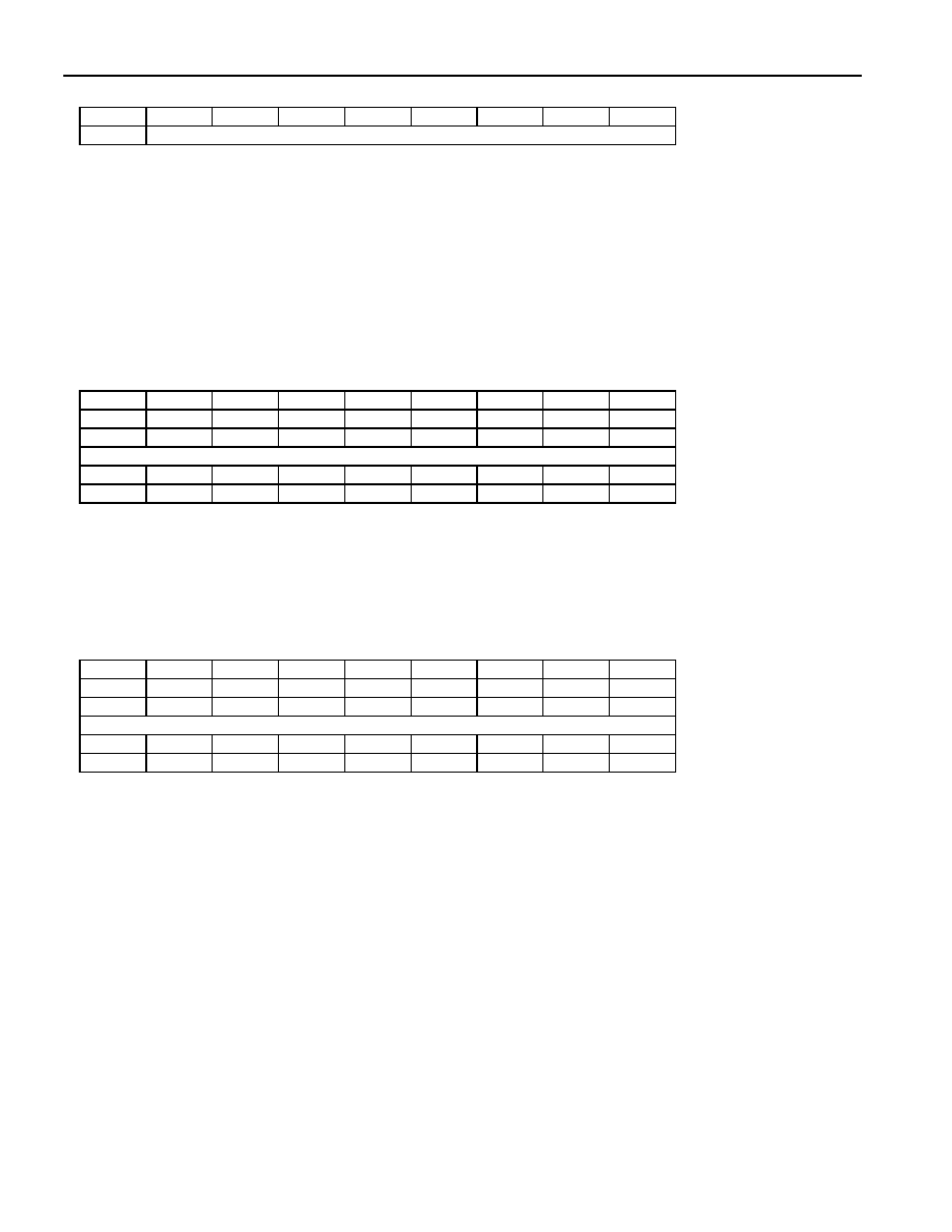
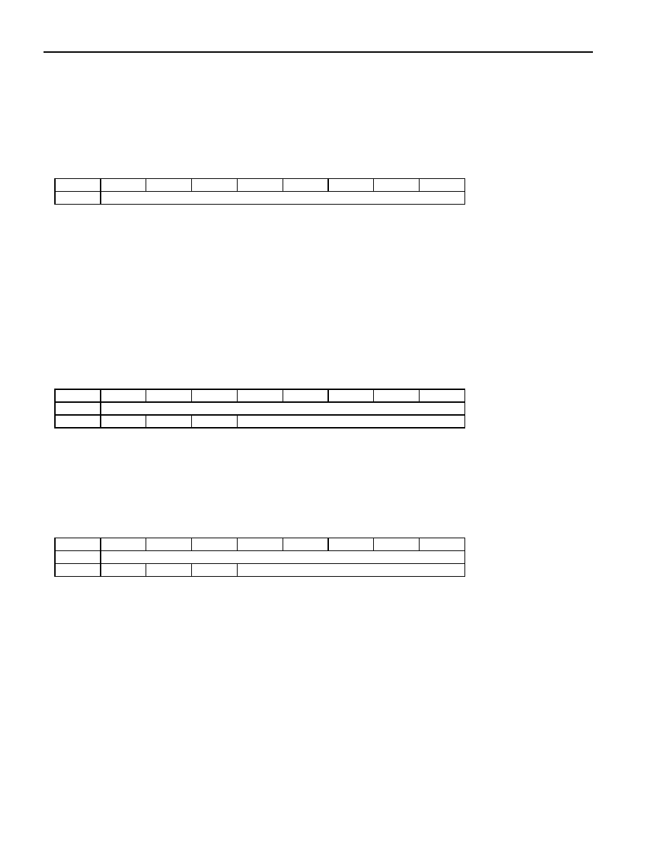
DATALOG MEMORY USAGE
Once setup for a mission, the DS2422 logs the temperature measurements and/or external data at equidistant time
points entry after entry in its datalog memory. The datalog memory is able to store 8192 entries in 8-bit format or
4096 entries in 16-bit format (Figure 10A). If temperature as well as external data is logged, both in the same
format, the memory is split into two equal sections that can store 4096 8-bit entries or 2048 16-bit entries (Figure
10B). If the device is set up to log data in different formats, e. g., temperature in 8-bit and external data in 16-bit
format, the memory is split into blocks of different size, accommodating 2560 entries for either data source (Figure
10C). In this case, the upper 256 bytes are not used. In 16-bit format, the higher 8 bits of an entry are stored at the
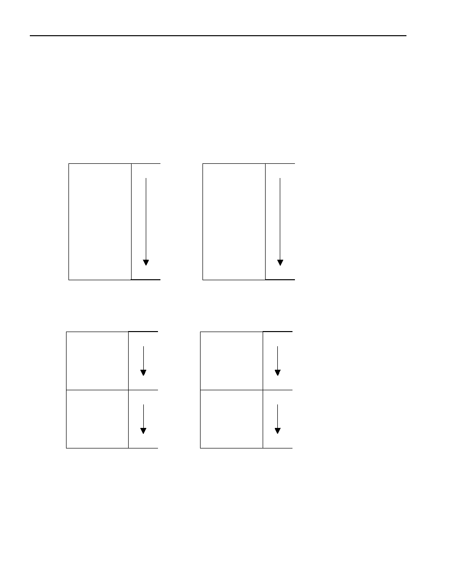
DS2422
23 of 48
lower address. Knowing the starting time point (Mission Time Stamp) and the interval between temperature
measurements one can reconstruct the time and date of each measurement.
There are two alternatives to the way the DS2422 behaves after the datalog memory is filled with data. The user
can program the device to either stop any further recording (disable "rollover") or overwrite the previously recorded
data (enable "rollover"), one entry at a time, starting again at the beginning of the respective memory section. The
contents of the Mission Samples Counter in conjunction with the sample rate and the Mission Time Stamp will then
allow reconstructing the time points of all values stored in the datalog memory. This gives the exact history over
time for the most recent measurements taken. Earlier measurements cannot be reconstructed.
Figure 10A. One-Channel Logging
8192
8-bit entries
Temperature
or
External data
4096
16-bit entries
Temperature
or
External data
1000h
2FFFh
1000h
2FFFh
ETL = 1; EDL = 0 or
ETL = 0; EDL = 1
TLFS = DLFS = 0
ETL = 1; EDL = 0 or
ETL = 0; EDL = 1
TLFS = DLFS = 1
With 16-bit format,
the most-significant
byte is stored at the
lower address.
Figure 10B. Two-Channel Logging, Equal Resolution
Temperature
4096
8-bit entries
External Data
4096
8-bit entries
Temperature
2048
16-bit entries
External Data
2048
16-bit entries
1FFFh
2000h
1000h
2FFFh
1FFFh
2000h
1000h
2FFFh
ETL = EDL = 1
TLFS = DLFS = 0
ETL = EDL = 1
TLFS = DLFS = 1
With 16-bit format,
the most-significant
byte is stored at the
lower address.
DS2422
24 of 48
Figure 10C. Two-Channel Logging, Different Resolution
2E00h
2FFFh
Temperature
2560
8-bit entries
External Data
2560
16-bit entries
(not used)
External Data
2560
8-bit entries
(not used)
Temperature
2560
16-bit entries
19FFh
1A00h
1000h
2DFFh
2E00h
2FFFh
2DFFh
2400h
1000h
23FFh
ETL = EDL = 1
TLFS = 0; DLFS = 1
ETL = EDL = 1
TLFS = 1; DLFS = 0
With 16-bit format,
the most-significant
byte is stored at the
lower address.
MISSIONING
The typical task of the DS2422 is recording temperature and/or external data. Before the device can perform this
function, it needs to be set up properly. This procedure is called missioning.
First of all, DS2422 needs to have its RTC set to valid time and date. This reference time may be the local time, or,
when used inside of a mobile unit, UTC (also called GMT, Greenwich Mean Time) or any other time standard that
was agreed upon. The RTC oscillator must be running (EOSC = 1). The memory assigned to store the Mission
Time Stamp, Mission Samples Counter, Sample Rate, and Alarm Flags must be cleared using the Memory Clear
command. To enable the device for a mission, at least one of the enable logging bits needs to be set to 1. These
are general settings that have to be made in any case, regardless of the type of object to be monitored and the
duration of the mission.
If alarm signaling is desired, the temperature alarm and/or data alarm low and high thresholds must be defined.
How to convert a temperature value into the binary code to be written to the threshold registers is described under
Temperature Conversion earlier in this document. Determining the thresholds for the data alarm depends on the
hardware/converter that is connected to the DS2422's serial input. In addition, the temperature and/or data alarm
must be enabled for the low- and/or high-threshold. This makes the device respond to a Conditional Search
command (see ROM Function Commands), provided that an alarming condition has been encountered.
The setting of the RO bit (rollover enable) and sample rate depends on the duration of the mission and the
monitoring requirements. If the most recently logged data is important, the rollover should be enabled (RO = 1).
Otherwise one should estimate the duration of the mission in minutes and divide the number by 8192 (single
channel 8-bit format) or 4096 (single channel 16-bit format, two channels 8-bit format) or 2048 (two channels 16-bit
format) or 2560 (two channels, one 8-bit format and one 16-bit format) to calculate the value of the sample rate
(number of minutes between temperature conversions). If the estimated duration of a mission is 10 days (= 14400
minutes), for example, then the 8192-byte capacity of the datalog memory would be sufficient to store a new 8-bit
value every 1.8 minutes (110 seconds). If the datalog memory of the DS2422 is not large enough to store all
readings, one can use several devices and set the Mission Start Delay to values that make the second device start
logging as soon as the memory of the first device is full, and so on. The RO-bit needs to be set to 0 to disable
rollover that would otherwise overwrite the logged data.
After the RO bit and the Mission Start Delay are set, the sample rate needs to be written to the Sample Rate
Register. The sample rate may be any value from 1 to 16383, coded as an unsigned 14-bit binary number. A
sample rate of all zeros is not valid and must be avoided under all circumstances. This causes the device to enter
into an undefined state, requiring a power-on reset and restore of the trim settings to recover. The fastest sample
rate is one sample per second (EHSS = 1, Sample Rate = 0001h) and the slowest is one sample every 273.05
hours (EHSS = 0, Sample Rate =3 FFFh). To get one sample every 6 minutes, for example, the sample rate value
needs to be set to 6 (EHSS = 0) or 360 decimal (equivalent to 0168h at EHSS = 1).

DS2422
25 of 48
If there is a risk of unauthorized access to the DS2422 or manipulation of data, one should define passwords for
read access and full access. Before the passwords become effective, their use needs to be enabled. See Security
by Password for more details.
The last step to begin a mission is to issue the Start Mission command. As soon as it has received this command,
the DS2422 sets the MIP flag and clear the MEMCLR flag. With the immediate/delayed start mode (SUTA = 0),
after as many minutes as specified by the Mission Start Delay are over, the device wakes up, copy the current date
and time to the mission time stamp register, and log the first entry of the mission. This increments both the Mission
Samples Counter and Device Samples Counter. All subsequent log entries are made as specified by the value in
the Sample Rate Register and the EHSS bit.
If the Start Upon Temperature Alarm mode is chosen (SUTA = 1
,
ETL = 1) the DS2422 will first wait until the start
delay is over. Then the device wakes up in intervals as specified by the sample rate and EHSS bit and measure the
temperature. This increments the device samples counter only. Only after an alarming temperature is encountered
does the DS2422 set the mission time stamp. The first sample of the mission is logged one sample period after the
temperature alarm occurred.
From then on, both the Mission Samples Counter and Device Samples Counter
increments at the same time. All subsequent log entries are made as specified by the value in the Sample Rate
Register and the EHSS bit.
The general-purpose memory operates independently of the other memory sections and is not write-protected
during a mission. All memory of the DS2422 can be read at any time, e. g., to watch the progress of a mission.
Attempts to read the passwords will read 00h bytes instead of the data that is stored in the password registers.
ADDRESS REGISTERS AND TRANSFER STATUS
Because of the serial data transfer, the DS2422 employs three address registers, called TA1, TA2, and E/S (Figure
11). Registers TA1 and TA2 must be loaded with the target address to which the data is written or from which data
is sent to the master upon a Read command. Register E/S acts like a byte counter and transfer status register. It is
used to verify data integrity with Write commands. Therefore, the master only has read access to this register. The
lower 5 bits of the E/S Register indicate the address of the last byte that has been written to the scratchpad. This
address is called Ending Offset. The DS2422 requires that the Ending Offset is always 1Fh for a Copy
Scratchpad to function.
Bit 5 of the E/S Register, called PF or "partial byte flag," is set if the number of data bits
sent by the master is not an integer multiple of 8. Bit 6 is always a 0. Note that the lowest 5 bits of the target
address also determine the address within the scratchpad, where intermediate storage of data will begin. This
address is called byte offset. If the target address for a Write command is 13Ch, for example, then the scratchpad
will store incoming data beginning at the byte offset 1Ch and will be full after only 4 bytes. The corresponding
ending offset in this example is 1Fh. For best economy of speed and efficiency, the target address for writing
should point to the beginning of a new page, i.e., the byte offset will be 0. Thus the full 32-byte capacity of the
scratchpad is available, resulting also in the ending offset of 1Fh. However, it is possible to write 1 or several
contiguous bytes somewhere within a page. The ending offset together with the Partial and Overflow Flag is mainly
a means to support the master checking the data integrity after a Write command. The highest valued bit of the E/S
Register, called AA or Authorization Accepted, indicates that a valid copy command for the scratchpad has been
received and executed. Writing data to the scratchpad clears this flag.
Figure 11. Address Registers
Bit #
7
6
5
4
3
2
1
0
Target Address (TA1)
T7
T6
T5
T4
T3
T2
T1
T0
Target Address (TA2)
T15
T14
T13
T12
T11
T10
T9
T8
Ending Address with
Data Status (E/S)
(Read Only)
AA
0
PF
E4
E3
E2
E1
E0

DS2422
26 of 48
WRITING WITH VERIFICATION
To write data to the DS2422, the scratchpad has to be used as intermediate storage. First the master issues the
Write Scratchpad command to specify the desired target address, followed by the data to be written to the
scratchpad. In the next step, the master sends the Read Scratchpad command to read the scratchpad and to verify
data integrity. As preamble to the scratchpad data, the DS2422 sends the requested target address TA1 and TA2
and the contents of the E/S Register. If the PF flag is set, data did not arrive correctly in the scratchpad. The
master does not need to continue reading; it can start a new trial to write data to the scratchpad. Similarly, a set AA
flag indicates that the Write command was not recognized by the device. If everything went correctly, both flags are
cleared and the ending offset indicates the address of the last byte written to the scratchpad. Now the master can
continue verifying every data bit. After the master has verified the data, it has to send the Copy Scratchpad
command. This command must be followed exactly by the data of the three address registers TA1, TA2 and E/S as
the master has read them verifying the scratchpad. As soon as the DS2422 has received these bytes, it will copy
the data to the requested location beginning at the target address.
MEMORY- AND CONTROL-FUNCTION COMMANDS
The "Memory/Control Function Flow Chart" (Figure 12) describes the protocols necessary for accessing the
memory and the special function registers of the DS2422. An example on how to use these and other functions to
set up the DS2422 for a mission is included at the end of this document, preceding the Electrical Characteristics
section. The communication between master and DS2422 takes place either at regular speed (default, OD = 0) or
at Overdrive Speed (OD = 1). If not explicitly set into the Overdrive Mode the DS2422 assumes regular speed.
Internal memory access during a mission has priority over external access through the 1-Wire interface. This
affects several of the commands described below. See section Memory Access Conflicts for details and remedies.
WRITE SCRATCHPAD COMMAND [0Fh]
After issuing the Write Scratchpad command, the master must first provide the 2-byte target address, followed by
the data to be written to the scratchpad. The data is written to the scratchpad starting at the byte offset (T4:T0).
The master has to send as many bytes as are needed to reach the Ending Offset of 1Fh. If a data byte is
incomplete, its content is ignored and the partial byte flag PF is set.
When executing the Write Scratchpad command the CRC generator inside the DS2422 (see Figure 18) calculates
a CRC of the entire data stream, starting at the command code and ending at the last data byte sent by the master.
This CRC is generated using the CRC16 polynomial by first clearing the CRC generator and then shifting in the
command code (0Fh) of the Write Scratchpad command, the Target Addresses TA1 and TA2 as supplied by the
master and all the data bytes. The master may end the Write Scratchpad command at any time. If the ending offset
is 11111b, the master may send 16 read-time slots and receives the inverted CRC16 generated by the DS2422.
Note that both register pages are write-protected during a mission. Although the Write Scratchpad command works
normally at any time, the subsequent copy scratchpad to a register page will fail during a mission.
READ SCRATCHPAD COMMAND [AAh]
This command is used to verify scratchpad data and target address. After issuing the Read Scratchpad command,
the master begins reading. The first 2 bytes will be the target address. The next byte will be the ending offset/data
status byte (E/S) followed by the scratchpad data beginning at the byte offset (T4:T0), as shown in Figure 11. The
master may continue reading data until the end of the scratchpad after which it will receive an inverted CRC16 of
the command code, Target Addresses TA1 and TA2, the E/S byte, and the scratchpad data starting at the target
address. After the CRC is read, the bus master will read logical 1s from the DS2422 until a reset pulse is issued.

DS2422
27 of 48
COPY SCRATCHPAD WITH PASSWORD [99h]
This command is used to copy data from the scratchpad to the writable memory sections. After issuing the Copy
Scratchpad command, the master must provide a 3-byte authorization pattern, which can be obtained by reading
the scratchpad for verification. This pattern must exactly match the data contained in the three address registers
(TA1, TA2, E/S, in that order). Next the master must transmit the 64-bit full-access password. If passwords are
enabled and the transmitted password is different from the stored full-access password, the Copy Scratchpad with
Password command will fail. The device will stop communicating and will wait for a reset pulse. If the password
was correct or if passwords were not enabled, the device will test the 3-byte authorization code. If the authorization
code pattern matches, the AA (Authorization Accepted) flag will be set and the copy will begin. A pattern of
alternating 1s and 0s will be transmitted after the data has been copied until the master issues a reset pulse. While
the copy is in progress any attempt to reset the part will be ignored. Copy typically takes 2µs per byte.
The data to be copied is determined by the three address registers. The scratchpad data from the beginning offset
through the ending offset will be copied, starting at the target address. Anywhere from 1 to 32 bytes may be copied
to memory with this command. The AA flag will remain at logic 1 until it is cleared by the next Write Scratchpad
command. With suitable password, the copy scratchpad will always function for the 16 pages of data memory and
the 2 pages of calibration memory. While a mission is in progress, write attempts to the register pages will not be
successful. The AA bit (Authorization Accepted) remaining at 0 will indicate this.
READ MEMORY WITH PASSWORD AND CRC [69h]
The Read Memory with CRC command is the general function to read from the device. This command generates
and transmits a 16-bit CRC following the last data byte of a memory page.
After having sent the command code of the Read Memory with CRC command, the bus master sends a 2-byte
address that indicates a starting byte location. Next the master must transmit one of the 64-bit passwords. If
passwords are enabled and the transmitted password does not match one of the stored passwords, the Read
Memory with Password and CRC command will fail. The device will stop communicating and will wait for a reset
pulse. If the password was correct or if passwords were not enabled, the master reads data from the DS2422
beginning from the starting address and continuing until the end of a 32-byte page is reached. At that point the bus
master will send 16 additional read data time slots and receive the inverted 16-bit CRC. With subsequent read data
time slots the master will receive data starting at the beginning of the next memory page followed again by the
CRC for that page. This sequence will continue until the bus master resets the device. When trying to read the
passwords or memory areas that are marked as "reserved", the DS2422 will transmit 00h or FFh bytes
respectively. The CRC at the end of a 32-byte memory page is based on the data as it was transmitted.
With the initial pass through the Read Memory with CRC flow, the 16-bit CRC value is the result of shifting the
command byte into the cleared CRC generator followed by the 2 address bytes and the contents of the data
memory. Subsequent passes through the Read Memory with CRC flow will generate a 16-bit CRC that is the result
of clearing the CRC generator and then shifting in the contents of the data memory page. After the 16-bit CRC of
the last page is read, the bus master will receive logical 1s from the DS2422 until a reset pulse is issued. The Read
Memory with CRC command sequence can be ended at any point by issuing a reset pulse.
DS2422
28 of 48
Figure 12-1. Memory/Control Function Flow Chart
Master TX Memory or
Control Fkt. Command
0FH
Write
Scratchpad
Master TX
TA1 (T7:T0)
Master TX
TA2 (T15:T8)
DS2422 sets Scratch-
pad Offset = (T4:T0)
and Clears (PF, AA)
Master TX Data Byte
to Scratchpad Offset
DS2422 sets (E4:E0)
= Scratchpad Offset
Master
TX Reset?
Scratch-
pad Offset =
11111b?
Master RX CRC16 of
Command, Address Data
DS2422 Incre-
ments Scratch-
pad Offset
Master RX "1"s
Master
TX Reset?
Master
TX Reset?
Partial
Byte Written?
PF = 1
AAH
Read
Scratchpad
Master RX
TA1 (T7:T0)
Master RX
TA2 (T15:T8)
Master RX Ending
Offset with Data
Status (E/S)
Master
TX Reset?
Scratch-
pad Offset =
11111b?
Master RX CRC16 of
Command, Address Data,
E/S Byte, and Data Starting
at the Target Address
DS2422 Incre-
ments Scratch-
pad Offset
Master RX "1"s
Master
TX Reset?
DS2422 sets Scratch-
pad Offset = (T4:T0)
Master RX Data Byte
from Scratchpad Offset
From ROM Functions
Flow Chart (Figure 14)
To ROM Functions
Flow Chart (Figure 14)
N
Y
N
Y
N
Y
N
Y
N
Y
N
Y
N
Y
N
Y
N
Y
N
Y
From Figure 12
2
nd
Part
To Figure 12
2
nd
Part
DS2422
29 of 48
Figure 12-2. Memory/Control Function Flow Chart
99H
Copy Scrpd.
[w/PW]
Master TX
E/S Byte
Authorization
Code Match?
DS2422 Copies Scratchpad
Data to Memory
Copying
Finished
Master
TX Reset?
AA = 1
Master TX
TA1 (T7:T0), TA2 (T15:T8)
Master TX
64-Bits [Password]
Password
Accepted?
Master
RX "1"s
DS2422 TX "0"
DS2422 TX "1"
Master
TX Reset?
N
Y
N
Y
N
Y
N
Y
Master
TX Reset?
Master
RX "1"s
N
Y
N
Y
N
Y
Authorization
Code
From Figure 12
3
rd
Part
To Figure 12
3
rd
Part
To Figure 12
1
st
Part
From Figure 12
1
st
Part
DS2422
30 of 48
Figure 12-3. Memory/Control Function Flow Chart
69H
Read Mem.
[w/PW]&CRC
Master TX
64-Bits [Password]
Master
TX Reset?
CRC OK?
Master RX "1"s
DS2422 sets Memory
Address = (T15:T0)
Master RX Data Byte
from Memory Address
Master TX
TA1 (T7:T0), TA2 (T15:T8)
Password
Accepted?
DS2422 Incre-
ments Address
Counter
End of Page?
Master RX CRC16 of
Command, Address, Data
(1
st
Pass); CRC16 of Data
(Subsequent Passes)
End of
Memory?
Master TX
Reset?
Master TX
Reset
N
Y
N
Y
N
Y
N
Y
N
Y
N
Y
N
Y
Decision made
by DS2422
Decision made
by Master
From Figure 12
4
th
Part
To Figure 12
4
th
Part
To Figure 12
2
nd
Part
From Figure 12
2
nd
Part

DS2422
31 of 48
Figure 12-4. Memory/Control Function Flow Chart
96H
Clear Mem.
[w/PW]
55H
Forced
Conversion?
Master TX
64-Bits [Password]
N
Y
N
Y
Mission in
Progress?
DS2422 clears Mission
Time Stamp, Mission
Samples Counter,
Alarm Flags
DS2422 sets
MEMCLR = 1
Password
Accepted?
Master
TX Reset?
N
Y
N
Y
N
Y
Mission in
Progress?
DS2422 Performs a
Temp. Conversion
DS2422 copies Result
to Address 020C/Dh
DS2422 Reads Serial
Data Interface
DS2422 copies Result
to Address 020E/Fh
N
Y
Master
TX Reset?
N
Y
Master TX
FFh dummy byte
Master TX
FFh dummy byte
From Figure 12
5
th
Part
To Figure 12
5
th
Part
To Figure 12
3
rd
Part
From Figure 12
3
rd
Part
DS2422
32 of 48
Figure 12-5. Memory/Control Function Flow Chart
N
CCH
Start Mission
[w/PW]
Master TX
64-Bits [Password]
Master
TX Reset?
DS2422 Initiates
Mission Start Delay
Process
N
Y
Mission in
Progress?
DS2422 sets
MIP = 1
MEMCLR = 0
Password
Accepted?
MEMCLR
= 1?
N
Y
N
Y
N
Y
N
Y
Master TX
FFh dummy byte
33H
Stop Mission
[w/PW]
Master TX
64-Bits [Password]
N
Y
Mission in
Progress?
DS2422 sets
MIP = 0
WFTA = 0
Password
Accepted?
Master
TX Reset?
N
Y
N
Y
N
Y
Master TX
FFh dummy byte
DS2422 Waits for 1 Minute
Mission Start
Delay Process
DS2422 Sets WFTA=1
Start Delay
Counter = 0?
Y
DS2422 decrements
Start Delay Counter
DS2422 copies RTC
Data to Mission Time
Stamp Register
DS2422 Starts Logging
Taking First Sample
End Of Process
DS2422 sets WFTA=0
N
Y
Temp.
Alarm?
DS2422 Performs 8-bit
Temp. Conversion
N
MIP = 0?
Y
DS2422 Waits One
Sample Period
SUTA = 1?
Y
N
DS2422 Waits One
Sample Period
To Figure 12
4
th
Part
From Figure 12
4
th
Part

DS2422
33 of 48
CLEAR MEMORY WITH PASSWORD [96h]
The Clear Memory with Password command is used to prepare the device for another mission. This command will
only be executed if no mission is in progress. After the command code the master must transmit the 64-bit full-
access password followed by a FFh dummy byte. If passwords are enabled and the transmitted password is differ-
ent from the stored full-access password or a mission is in progress, the Clear Memory with Password command
will fail. The device will stop communicating and will wait for a reset pulse. If the password was correct or if
passwords were not enabled, the device will clear the Mission Time Stamp, Mission Samples Counter, Sample
Rate register, and all alarm flags of the Alarm Status Register. After these cells are cleared, the MEMCLR bit of the
General Status Register will read 1 to indicate the successful execution of the Clear Memory with Password
command. Clearing of the datalog memory is not necessary because the Mission Samples Counter indicates how
many entries in the datalog memory are valid.
FORCED CONVERSION [55h]
The Forced Conversion command can be used to measure the temperature and read data from the serial data
interface without starting a mission. After the command code the master has to send one FFh byte to get the
conversion started. The conversion result is found as 16-bit value in the Latest Temperature Conversion Result and
Latest Serial Data Reading
registers. This command is only executed if no mission is in progress (MIP = 0). It
cannot be interrupted and takes maximum 666 ms to complete. During this time memory access through the 1-
Wire interface is blocked. The device will behave the same way as during a mission when the sampling interferes
with a memory/control function command. See Memory Access Conflicts for details. A forced conversion must not
be attempted while the RTC oscillator is stopped. This causes the device to enter into an undefined state, requiring
a power-on reset and restore of the trim settings to recover.
START MISSION WITH PASSWORD [CCh]
The DS2422 uses a control function command to start a mission. A new mission can only be started if the previous
mission has been ended and the memory has been cleared. After the command code, the master must transmit the
64-bit full-access password followed by a FFh dummy byte. If passwords are enabled and the transmitted
password is different from the stored full-access password or a mission is in progress, the Start Mission with
Password command will fail. The device will stop communicating and will wait for a reset pulse. If the password
was correct or if passwords were not enabled, the device will start a mission. The sampling and data logging will
begin as soon as the mission start delay is over (SUTA = 0) and, if SUTA = 1, one sample period after a
temperature alarm was encountered. While the device is waiting for a temperature alarm to occur, the WFTA flag in
the general status register will read 1. During a mission there is only read access to the Register Pages.
STOP MISSION WITH PASSWORD [33h]
The DS2422 uses a control function command to stop a mission. Only a mission that is in progress can be
stopped. After the command code, the master must transmit the 64-bit full-access password followed by a FFh
dummy byte. If passwords are enabled and the transmitted password is different from the stored full-access
password or a mission is not in progress, the Stop Mission with Password command will fail. The device will stop
communicating and will wait for a reset pulse. If the password was correct or if passwords were not enabled, the
device will clear the MIP bit in the General Status Register and restore write access to the Register Pages. The
WFTA bit is not cleared. See the description of the General Status Register for a method to clear the WFTA bit.
MEMORY ACCESS CONFLICTS
While a mission is in progress or while the device is waiting for a temperature alarm to start a mission, periodically
a temperature sample is taken and/or data is read from the serial interface and logged. This "internal activity" has
priority over 1-Wire communication. As a consequence, device-specific commands (excluding ROM function
commands and 1-Wire reset) will not perform properly when internal and "external" activities interfere with each
other. Not affected are the commands Start Mission, Forced Conversion and Clear Memory, because they are not
applicable while a mission is in progress or while the device is waiting for a temperature alarm. The table below
explains how the remaining five commands are affected by internal activity, how to detect this interference and how
to work around it.

DS2422
34 of 48
COMMAND
INDICATION OF
INTERFERENCE
REMEDY
Write Scratchpad
The CRC16 at the end of the
command flow reads FFFFh.
Wait 0.5 seconds, 1-Wire reset, address the device,
repeat Write Scratchpad with the same data and check
the validity of the CRC16 at the end of the command
flow. Alternatively, use Read Scratchpad to verify data
integrity.
Read Scratchpad
The data read changes to FFh
bytes or all bytes received are
FFh, including the CRC at the
end of the command flow.
Wait 0.5 seconds, 1-Wire reset, address the device,
repeat Read Scratchpad and check the validity of the
CRC16 at the end of the command flow.
Copy Scratchpad
The device behaves as if
Authorization Code or pass-
word was not valid or as if the
copy function would not end.
Wait 0.5 seconds, 1-Wire reset, address the device,
issue Read Scratchpad and check the AA-bit of the
E/S byte. If the AA-bit is set, Copy Scratchpad was
successful.
Read Memory with
CRC
The data read changes to all
FFh bytes or all bytes received
are FFh, including the CRC at
the end of the command flow,
despite a valid password.
Wait 0.5 seconds, 1-Wire reset, address the device,
repeat Read Memory with CRC and check the validity
of the CRC16 at the end of the memory page.
Stop Mission
The general Status register at
address 215h reads FFh or the
MIP bit is 1 while bits 0, 2, and
5 are 0.
Wait 0.5 seconds, 1-Wire reset, address the device,
and repeat Stop Mission. Perform a 1-Wire reset,
address the device, read the general Status register at
address 215h and check the MIP-bit. If the MIP-bit is 0,
Stop Mission was successful.
The interference is more likely to be seen with a high sample rate (1 sample every second) and with high-resolution
logging, which can last up to 666ms when both temperature and external data are recorded. With lower sample
rates interference may hardly be visible at all. In any case, when writing driver software, it is important to know
about the possibility of interference and to take measures to work around it.
1-Wire BUS SYSTEM
The 1-Wire bus is a system, which has a single bus master and one or more slaves. In all instances the DS2422 is
a slave device. The bus master is typically a microcontroller. The discussion of this bus system is broken down into
three topics: hardware configuration, transaction sequence, and 1-Wire signaling (signal types and timing). The
1-Wire protocol defines bus transactions in terms of the bus state during specific time slots that are initiated on the
falling edge of sync pulses from the bus master. For a more detailed protocol description, refer to Chapter 4 of the
Book of DS19xx iButton Standards.
HARDWARE CONFIGURATION
The 1-Wire bus has only a single line by definition; it is important that each device on the bus be able to drive it at
the appropriate time. To facilitate this, each device attached to the 1-Wire bus must have open drain or tri-state
outputs. The 1-Wire port of the DS2422 is open-drain with an internal circuit equivalent to that shown in Figure 13.
A multidrop bus consists of a 1-Wire bus with multiple slaves attached. At standard speed the 1-Wire bus has a
maximum data rate of 16.3kbps. The speed can be boosted to 142kbps by activating the Overdrive mode. The
DS2422 is not guaranteed to be fully compliant to the iButton Standard. Its maximum data rate in standard speed
mode is 15.4kbps and 125kbps in Overdrive. The value of the pullup resistor primarily depends on the network size
and load conditions. The DS2422 requires a pullup resistor of maximum 2.2k
W at any speed.
The idle state for the 1-Wire bus is high. If for any reason a transaction needs to be suspended, the bus MUST be
left in the idle state if the transaction is to resume. If this does not occur and the bus is left low for more than 16µs
(Overdrive speed) or more than 120µs (standard speed), one or more devices on the bus may be reset. Note that
the DS2422 does not quite meet the full 16µs maximum low time of the normal 1-Wire bus Overdrive timing. With
the DS2422 the bus must be left low for no longer than 12µs at Overdrive to ensure that no DS2422 on the 1-Wire
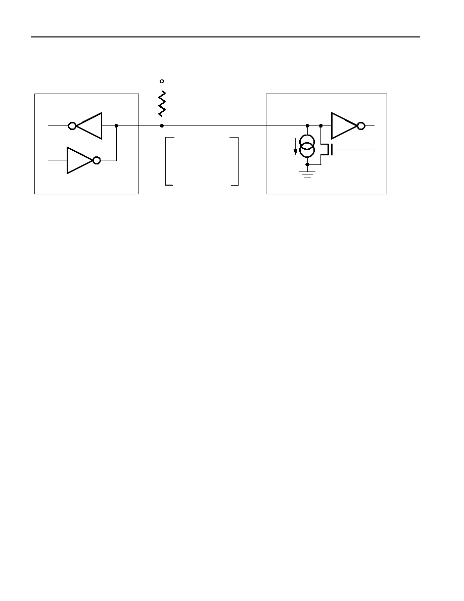
DS2422
35 of 48
bus performs a reset. The DS2422 will communicate properly when used in conjunction with a DS2480B or
DS2490 1-Wire driver and adapters that are based on these driver chips.
Figure 13. Hardware Configuration
Open Drain
Port Pin
RX = RECEIVE
TX = TRANSMIT
100 W
MOSFET
V
PUP
RX
TX
TX
RX
DATA
R
PUP
5 µA
Typ.
BUS MASTER
DS2422 1-Wire PORT
TRANSACTION SEQUENCE
The protocol for accessing the DS2422 through the 1-Wire port is as follows:
ß Initialization
ß ROM
Function
Command
ß Memory/Control Function Command
ß Transaction/Data
INITIALIZATION
All transactions on the 1-Wire bus begin with an initialization sequence. The initialization sequence consists of a
reset pulse transmitted by the bus master followed by presence pulse(s) transmitted by the slave(s). The presence
pulse lets the bus master know that the DS2422 is on the bus and is ready to operate. For more details, see the
1-Wire Signaling section.

DS2422
36 of 48
1-Wire ROM FUNCTION COMMANDS
Once the bus master has detected a presence, it can issue one of the eight ROM function commands that the
DS2422 supports. All ROM function commands are 8 bits long. A list of these commands follows (refer to flowchart
in Figure 14).
READ ROM [33h]
This command allows the bus master to read the DS2422's 8-bit family code, unique 48-bit serial number, and 8-bit
CRC. This command can only be used if there is a single slave on the bus. If more than one slave is present on the
bus, a data collision will occur when all slaves try to transmit at the same time (open drain will produce a wired-
AND result). The resultant family code and 48-bit serial number will result in a mismatch of the CRC.
MATCH ROM [55h]
The Match ROM command, followed by a 64-bit ROM sequence, allows the bus master to address a specific
DS2422 on a multidrop bus. Only the DS2422 that exactly matches the 64-bit ROM sequence will respond to the
following memory function command. All other slaves will wait for a reset pulse. This command can be used with a
single or multiple devices on the bus.
SEARCH ROM [F0h]
When a system is initially brought up, the bus master might not know the number of devices on the 1-Wire bus or
their registration numbers. By taking advantage of the wired-AND property of the bus, the master can use a
process of elimination to identify the registration numbers of all slave devices. For each bit of the registration
number, starting with the least significant bit, the bus master issues a triplet of time slots. On the first slot, each
slave device participating in the search outputs the true value of its registration number bit. On the second slot,
each slave device participating in the search outputs the complemented value of its registration number bit. On the
third slot, the master writes the true value of the bit to be selected. All slave devices that do not match the bit
written by the master stop participating in the search. If both of the read bits are zero, the master knows that slave
devices exist with both states of the bit. By choosing which state to write, the bus master branches in the romcode
tree. After one complete pass, the bus master knows the registration number of a single device. Additional passes
identify the registration numbers of the remaining devices. Refer to Application Note 187: 1-Wire Search Algorithm
for a detailed discussion, including an example.
CONDITIONAL SEARCH [ECh]
The Conditional Search ROM command operates similarly to the Search ROM command except that only those
devices, which fulfill certain conditions, will participate in the search. This function provides an efficient means for
the bus master to identify devices on a multidrop system that have to signal an important event. After each pass of
the conditional search that successfully determined the 64-bit ROM code for a specific device on the multidrop bus,
that particular device can be individually accessed as if a Match ROM had been issued, since all other devices will
have dropped out of the search process and will be waiting for a reset pulse.
The DS2422 will respond to the conditional search if one of the five alarm flags of the Alarm Status Register
(address 0214h) reads 1. The data and temperature alarm will only occur if enabled (see Temperature Sensor
Alarm and Serial Input Alarm). The BOR alarm is always enabled. The first alarm that occurs will make the device
respond to the Conditional Search command.
SKIP ROM [CCh]
This command can save time in a single-drop bus system by allowing the bus master to access the memory
functions without providing the 64-bit ROM code. If more than one slave is present on the bus and, for example, a
Read command is issued following the Skip ROM command, data collision will occur on the bus as multiple slaves
transmit simultaneously (open drain pulldowns will produce a wired-AND result).
RESUME COMMAND [A5h]
The DS2422 needs to be accessed several times before a mission will start. In a multidrop environment this means
that the 64-bit ROM code after a Match ROM command has to be repeated for every access. To maximize the data
throughput in a multidrop environment, the Resume function was implemented. This function checks the status of
the RC bit and, if it is set, directly transfers control to the Memory/Control functions, similar to a Skip ROM

DS2422
37 of 48
command. The only way to set the RC bit is through successfully executing the Match ROM, Search ROM or
Overdrive Match ROM command. Once the RC bit is set, the device can repeatedly be accessed through the
Resume Command function. Accessing another device on the bus will clear the RC bit, preventing two or more
devices from simultaneously responding to the Resume Command function.
OVERDRIVE SKIP ROM [3Ch]
On a single-drop bus this command can save time by allowing the bus master to access the memory/control func-
tions without providing the 64-bit ROM code. Unlike the normal Skip ROM command, the Overdrive Skip ROM sets
the DS2422 in the Overdrive mode (OD = 1). All communication following this command has to occur at Overdrive
speed until a reset pulse of minimum 690µs duration resets all devices on the bus to standard speed (OD = 0).
When issued on a multidrop bus this command will set all Overdrive-supporting devices into Overdrive mode. To
subsequently address a specific Overdrive-supporting device, a reset pulse at Overdrive speed has to be issued
followed by a Match ROM or Search ROM command sequence. This will speed up the time for the search process.
If more than one slave supporting Overdrive is present on the bus and the Overdrive Skip ROM command is
followed by a Read command, data collision will occur on the bus as multiple slaves transmit simultaneously (open-
drain pulldowns will produce a wired-AND result).
OVERDRIVE MATCH ROM [69h]
The Overdrive Match ROM command followed by a 64-bit ROM sequence transmitted at Overdrive Speed allows
the bus master to address a specific DS2422 on a multidrop bus and to simultaneously set it in Overdrive mode.
Only the DS2422 that exactly matches the 64-bit ROM sequence will respond to the subsequent memory/control
function command. Slaves already in Overdrive mode from a previous Overdrive Skip or successful Overdrive
Match command will remain in Overdrive mode. All overdrive-capable slaves will return to standard speed at the
next Reset Pulse of minimum 690µs duration. The Overdrive Match ROM command can be used with a single or
multiple devices on the bus.

DS2422
38 of 48
Figure 14-1. ROM Functions Flow Chart
From Figure 14
2
nd
Part
To Memory Functions
Flow Chart (Figure 12)
Master TX Bit 0
Master TX Bit 63
Master TX Bit 1
RC = 1
DS2422 TX
CRC Byte
DS2422 TX
Serial Number
(6 Bytes)
DS2422 TX
Family Code
(1 Byte)
Bit 0
Match?
Y
N
Bit 1
Match?
Y
N
Bit 63
Match?
Y
N
DS2422 TX Bit 0
DS2422 TX Bit 0
Master TX Bit 0
DS2422 TX Bit 1
DS2422 TX Bit 1
Master TX Bit 1
DS2422 TX Bit 63
DS2422 TX Bit 63
Master TX Bit 63
RC = 1
Bit 0
Match?
Y
N
Bit 1
Match?
Y
N
Bit 63
Match?
Y
N
To Figure 14
2
nd
Part
RC = 0
RC = 0
RC = 0
RC = 0
Y
Y
Y
Y
N
F0h
Search ROM
Command?
N
55h
Match ROM
Command?
N
ECh
Cond. Search
Command?
N
33h
Read ROM
Command?
To Figure 14
2
nd
Part
From Memory Functions
Flow Chart (Figure 12)
Bus Master TX ROM
Function Command
DS2422 TX
Presence Pulse
OD
Reset Pulse?
N
Y
OD = 0
Bus Master TX
Reset Pulse
From Figure 14, 2
nd
Part
Condition Met?
Y
N
DS2422 TX Bit 0
DS2422 TX Bit 0
Master TX Bit 0
DS2422 TX Bit 1
DS2422 TX Bit 1
Master TX Bit 1
DS2422 TX Bit 63
DS2422 TX Bit 63
Master TX Bit 63
RC = 1
Bit 0
Match?
Y
N
Bit 1
Match?
Y
N
Bit 63
Match?
Y
N
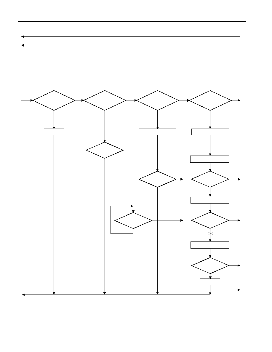
DS2422
39 of 48
Figure 14-2. ROM Functions Flow Chart
From Figure 14
1
st
Part
From Figure 14
1
st
Part
To Figure 14, 1
st
Part
RC = 1 ?
N
Y
RC = 0 ; OD = 1
Master TX Bit 0
Master TX Bit 63
Master TX Bit 1
RC = 1
Bit 0
Match?
Y
N
Bit 1
Match?
Y
N
Bit 63
Match?
Y
N
Y
N
69h
Overdrive Match
ROM?
RC = 0 ; OD = 1
Master
TX Reset ?
Y
N
Master
TX Reset ?
N
Y
Y
N
3Ch
Overdrive
Skip ROM?
Y
N
A5h
Resume
Command?
RC = 0
Y
N
CCh
Skip ROM
Command?
To Figure 14
1
st
Part
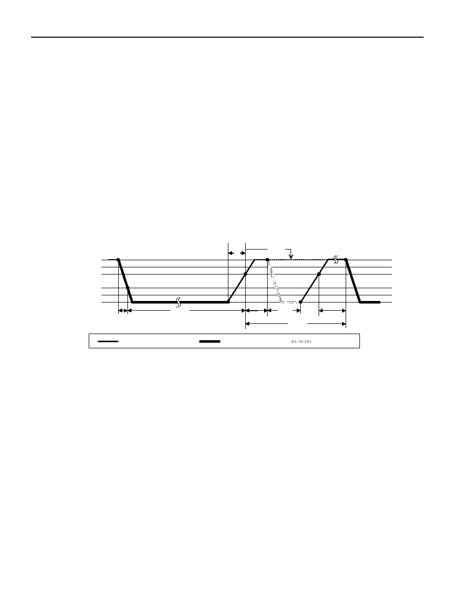
DS2422
40 of 48
1-Wire SIGNALING
The DS2422 requires strict protocols to ensure data integrity. The protocol consists of four types of signaling on
one line: Reset Sequence with Reset Pulse and Presence Pulse, Write-Zero, Write-One and Read-Data. Except for
the presence pulse the bus master initiates all these signals. The DS2422 can communicate at two different
speeds, standard speed, and Overdrive Speed. If not explicitly set into the Overdrive mode, the DS2422 will
communicate at standard speed. While in Overdrive Mode the fast timing applies to all waveforms.
To get from idle to active, the voltage on the 1-Wire line needs to fall from V
PUP
below the threshold V
TL
. To get
from active to idle, the voltage needs to rise from V
ILMAX
past the threshold V
TH
. The time it takes for the voltage to
make this rise is seen in Figure 15 as '
e' and its duration depends on the pull-up resistor (R
PUP
) used and the
capacitance of the 1-Wire network attached.
The voltage V
ILMAX
is relevant for the DS2422 when determining a
logical level, not triggering any events.
The initialization sequence required to begin any communication with the DS2422 is shown in Figure 15. A Reset
Pulse followed by a Presence Pulse indicates the DS2422 is ready to receive data, given the correct ROM and
memory function command. If the bus master uses slew-rate control on the falling edge, it must pull down the line
for t
RSTL
+ t
F
to compensate for the edge. A t
RSTL
duration of 690µs or longer will exit the Overdrive Mode returning
the device to standard speed. If the DS2422 is in Overdrive Mode and t
RSTL
is no longer than 80µs the device will
remain in Overdrive Mode.
Figure 15. Initialization Procedure "Reset and Presence Pulses"
RESISTOR
MASTER
DS2422
t
RSTL
t
PDL
t
RSTH
t
PDH
MASTER TX "RESET PULSE" MASTER RX "PRESENCE PULSE"
V
PUP
V
IHMASTER
V
TH
V
TL
V
ILMAX
0V
e
t
F
t
REC
t
MSP
After the bus master has released the line it goes into receive mode (RX). Now the 1-Wire bus is pulled to V
PUP
through the pullup resistor or, in case of a DS2480B driver, by active circuitry. When the threshold V
TH
is crossed,
the DS2422 waits for t
PDH
and then transmits a Presence Pulse by pulling the line low for t
PDL
. To detect a presence
pulse, the master must test the logical state of the 1-Wire line at t
MSP
.
The t
RSTH
window must be at least the sum of t
PDHMAX
, t
PDLMAX
, and t
RECMIN
. Immediately after t
RSTH
is expired, the
DS2422 is ready for data communication. In a mixed population network t
RSTH
should be extended to minimum
480µs at standard speed and 48µs at Overdrive speed to accommodate other 1-Wire devices.
Read/Write Time Slots
Data communication with the DS2422 takes place in time slots, which carry a single bit each. Write time slots
transport data from bus master to slave. Read time slots transfer data from slave to master. The definitions of the
write and read time slots are illustrated in Figure 16.
All communication begins with the master pulling the data line low. As the voltage on the 1-Wire line falls below the
threshold V
TL
, the DS2422 starts its internal timing generator that determines when the data line will be sampled
during a write time slot and how long data will be valid during a read time slot.
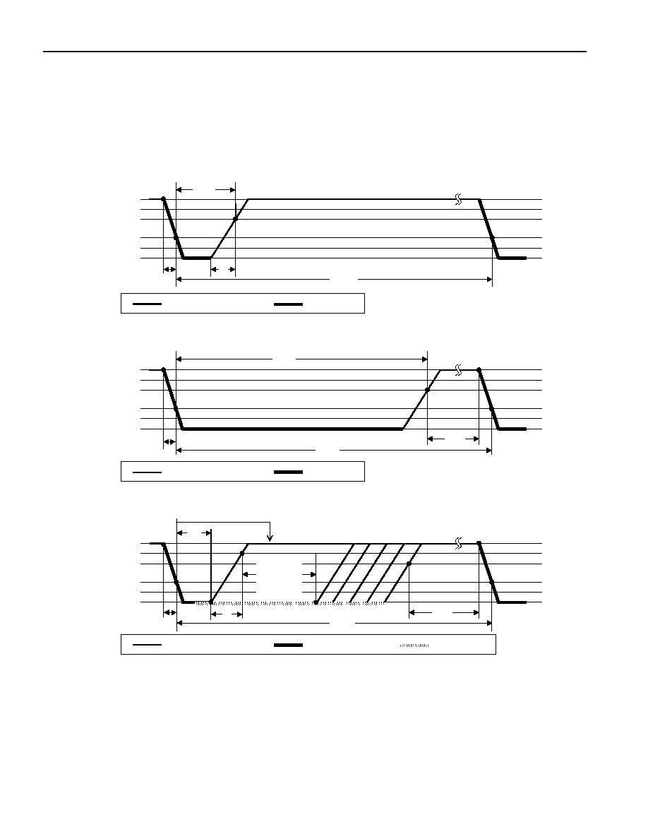
DS2422
41 of 48
Master-to-Slave
For a write-one time slot, the voltage on the data line must have crossed the V
TH
threshold before the write-one
low time t
W1LMAX
is expired. For a write-zero time slot, the voltage on the data line must stay below the V
TH
threshold until the write-zero low time t
W0LMIN
is expired. For most reliable communication the voltage on the data
line should not exceed V
ILMAX
during the entire t
W0L
or t
W1L
window. After the V
TH
threshold has been crossed, the
DS2422 needs a recovery time t
REC
before it is ready for the next time slot.
Figure 16. Read/Write Timing Diagram
Write-One Time Slot
RESISTOR
MASTER
V
PUP
V
IHMASTER
V
TH
V
TL
V
ILMAX
0V
t
F
t
SLOT
t
W1L
e
Write-Zero Time Slot
RESISTOR
MASTER
t
REC
V
PUP
V
IHMASTER
V
TH
V
TL
V
ILMAX
0V
t
F
t
SLOT
t
W0L
Read-Data Time Slot
RESISTOR
MASTER
DS2422
t
REC
V
PUP
V
IHMASTER
V
TH
V
TL
V
ILMAX
0V
Master
Sampling
Window
d
t
F
t
SLOT
t
RL
t
MSR
Slave-to-Master
A read-data time slot begins like a write-one time slot. The voltage on the data line must remain below V
TL
until the
read low time t
RL
is expired. During the t
RL
window, when responding with a 0, the DS2422 will start pulling the data
line low; its internal timing generator determines when this pulldown ends and the voltage starts rising again. When
responding with a 1, the DS2422 will not hold the data line low at all, and the voltage starts rising as soon as t
RL
is
over.
DS2422
42 of 48
The sum of t
RL
+
d (rise rime) on one side and the internal timing generator of the DS2422 on the other side define
the master sampling window (t
MSRMIN
to t
MSRMAX
) in which the master must perform a read from the data line. For
most reliable communication, t
RL
should be as short as permissible and the master should read close to but no later
than t
MSRMAX
. After reading from the data line, the master must wait until t
SLOT
is expired. This guarantees sufficient
recovery time t
REC
for the DS2422 to get ready for the next time slot.
IMPROVED NETWORK BEHAVIOR
In a 1-Wire environment line termination is possible only during transients controlled by the bus master (1-Wire
driver). 1-Wire networks, therefore, are susceptible to noise of various origins. Depending on the physical size and
topology of the network, reflections from end points and branch points can add up or cancel each other to some
extent. Such reflections are visible as glitches or ringing on the 1-Wire communication line. Noise coupled onto the
1-Wire line from external sources can also result in signal glitching. A glitch during the rising edge of a time slot can
cause a slave device to lose synchronization with the master and, as a consequence, result in a search ROM
command coming to a dead end or cause a device-specific function command to abort. For better performance in
network applications, the DS2422 uses a new 1-Wire front end, which makes it less sensitive to noise and also
reduces the magnitude of noise injected by the slave device itself.
The 1-Wire front end of the DS2422 differs from traditional slave devices in four characteristics.
1) The falling edge of the presence pulse has a controlled slew rate. This provides a better match to the line
impedance than a digitally switched transistor, converting the high frequency ringing known from traditional
devices into a smoother low-bandwidth transition. The slew rate control is specified by the parameter t
FPD
,
which has different values for standard and Overdrive speed.
2) There is additional low-pass filtering in the circuit that detects the falling edge at the beginning of a time slot.
This reduces the sensitivity to high-frequency noise. This additional filtering does not apply at Overdrive speed.
3) There is a hysteresis at the low-to-high switching threshold V
TH
. If a negative glitch crosses V
TH
but doesn't go
below V
TH
- V
HY
, it will not be recognized (Figure 17, Case A). The hysteresis is effective at any 1-Wire speed.
4) There is a time window specified by the rising edge hold-off time t
REH
during which glitches will be ignored,
even if they extend below V
TH
- V
HY
threshold (Figure 17, Case B, t
GL
< t
REH
). Deep voltage droops or glitches
that appear late after crossing the V
TH
threshold and extend beyond the t
REH
window cannot be filtered out and
will be taken as beginning of a new time slot (Figure 17, Case C, t
GL
≥ t
REH
).
Only devices which have the parameters t
FPD
, V
HY
and t
REH
specified in their electrical characteristics use the
improved 1-Wire front end.
Figure 17. Noise Suppression Scheme
V
PUP
V
TH
V
HY
0V
t
REH
t
GL
t
REH
t
GL
Case A
Case C
Case B
CRC GENERATION
With the DS2422 there are two different types of CRCs (Cyclic Redundancy Checks). One CRC is an 8-bit type
and is stored in the most significant byte of the 64-bit ROM. The bus master can compute a CRC value from the
first 56 bits of the 64-bit ROM and compare it to the value stored within the DS2422 to determine if the ROM data
has been received error-free. The equivalent polynomial function of this CRC is: X
8
+ X
5
+ X
4
+ 1. This 8-bit CRC is
received in the true (non-inverted) form. It is computed at the factory and lasered into the ROM.
The other CRC is a 16-bit type, generated according to the standardized CRC16-polynomial function x
16
+ x
15
+ x
2
+ 1. This CRC is used for error detection when reading register pages or the datalog memory using the Read
Memory with CRC command and for fast verification of a data transfer when writing to or reading from the
scratchpad. In contrast to the 8-bit CRC, the 16-bit CRC is always communicated in the inverted form. A CRC-
generator inside the DS2422 chip (Figure 18) will calculate a new 16-bit CRC as shown in the command flow chart
of Figure 12. The bus master compares the CRC value read from the device to the one it calculates from the data

DS2422
43 of 48
and decides whether to continue with an operation or to reread the portion of the data with the CRC error. With the
initial pass through the Read Memory with CRC flow chart, the 16-bit CRC value is the result of shifting the
command byte into the cleared CRC generator, followed by the 2 address bytes and the data bytes. The password
is excluded from the CRC calculation. Subsequent passes through the Read Memory with CRC flow chart will
generate a 16-bit CRC that is the result of clearing the CRC generator and then shifting in the data bytes
.
With the Write Scratchpad command the CRC is generated by first clearing the CRC generator and then shifting in
the command code, the Target Addresses TA1 and TA2 and all the data bytes. The DS2422 will transmit this CRC
only if the data bytes written to the scratchpad include scratchpad ending offset 11111b. The data may start at any
location within the scratchpad.
With the Read Scratchpad command the CRC is generated by first clearing the CRC generator and then shifting in
the command code, the Target Addresses TA1 and TA2, the E/S byte, and the scratchpad data starting at the
target address. The DS2422 will transmit this CRC only if the reading continues through the end of the scratchpad,
regardless of the actual ending offset. For more information on generating CRC values see Application Note 27.
Figure 18. CRC-16 Hardware Description and Polynomial
Polynomial = X
16
+ X
15
+ X
2
+ 1
X
0
X
1
X
2
X
3
X
4
X
5
X
6
X
7
X
8
X
9
X
10
X
11
X
12
X
13
X
14
X
15
X
16
1
st
STAGE
2
nd
STAGE
3
rd
STAGE
4
th
STAGE
6
th
STAGE
5
th
STAGE
7
th
STAGE
8
th
STAGE
9
th
STAGE
10
th
STAGE
11
th
STAGE
12
th
STAGE
13
th
STAGE
14
th
STAGE
15
th
STAGE
16
th
STAGE
INPUT DATA
CRC
OUTPUT
Figure 19. Crystal Placement on PCB
Local ground
plane beneath
signal plane or on
other side of pcb
Guard ring on
signal plane
Crystal
Pad
Crystal
Pad
VIA
AGND
X1
ALARM
X2

DS2422
44 of 48
COMMAND-SPECIFIC 1-Wire COMMUNICATION PROTOCOL--LEGEND
SYMBOL
DESCRIPTION
RST
1-Wire Reset Pulse generated by master
PD
1-Wire Presence Pulse generated by slave
Select
Command and data to satisfy the ROM function protocol
WS
Command "Write Scratchpad"
RS
Command "Read Scratchpad"
CPS
Command "Copy Scratchpad with Password"
RM
Command "Read Memory with Password"
RMC
Command "Read Memory with Password & CRC"
CM
Command "Clear Memory with Password "
FC
Command "Forced Conversion"
SM
Command "Start Mission with Password"
STP
Command "Stop Mission with Password"
TA
Target Address TA1, TA2
TA-E/S
Target Address TA1, TA2 with E/S byte
<data to EOS>
Transfer of as many data bytes as are needed to reach the scratchpad offset 1Fh
<data to EOP>
Transfer of as many data bytes as are needed to reach the end of a memory page
<data to EOM>
Transfer of as many data bytes as are needed to reach the end of the datalog memory
<PW/dummy>
Transfer of 8 bytes that either represent a valid password or acceptable dummy data
<32 bytes>
Transfer of 32 bytes
<data>
Transfer of an undetermined amount of data
FFh
Transmission of one byte FFh
CRC16\
Transfer of an inverted CRC16
FF loop
Indefinite loop where the master reads FF bytes
AA loop
Indefinite loop where the master reads AA bytes
COMMAND-SPECIFIC 1-Wire COMMUNICATION PROTOCOL--COLOR CODES
Master to slave
Slave to master
WRITE SCRATCHPAD, REACHING THE END OF THE SCRATCHPAD (CANNOT FAIL)
RST
PD
Select
WS
TA
<data to EOS>
CRC16\
FF loop
READ SCRATCHPAD (CANNOT FAIL)
RST
PD
Select
RS
TA-E/S
<data to EOS>
CRC16\
FF loop

DS2422
45 of 48
COPY SCRATCHPAD WITH PASSWORD (SUCCESS)
RST
PD
Select
CPS
TA-E/S
<PW/dummy>
AA loop
COPY SCRATCHPAD WITH PASSWORD (INVALID TA-E/S OR PASSWORD)
RST
PD
Select
CPS
TA-E/S
<PW/dummy>
FF loop
READ MEMORY WITH PASSWORD & CRC (SUCCESS)
RST
PD
Select
RMC
TA
<PW/dummy>
<data to EOP>
CRC16\
<32 bytes>
CRC16\
FF loop
READ MEMORY WITH PASSWORD & CRC (INVALID PASSWORD OR ADDRESS)
RST
PD
Select
RMC
TA
<PW/dummy>
FF loop
CLEAR MEMORY WITH PASSWORD
RST
PD
Select
CM
<PW/dummy>
FFh
FF loop
To verify success, read the General Status Register at address 0215h. If MEMCLR is 1, the command was
executed successfully.
FORCED CONVERSION
RST
PD
Select
FC
FFh
FF loop
To read the result and to verify success, read the addresses 020Ch to 020Fh (results) and the Device Samples
Counter at address 0223h to 0225h. If the count has incremented, the command was executed successfully.
START MISSION WITH PASSWORD
RST
PD
Select
SM
<PW/dummy>
FFh
FF loop
To verify success, read the General Status Register at address 0215h. If MIP is 1 and MEMCLR is 0, the command
was executed successfully.
Loop

DS2422
46 of 48
STOP MISSION WITH PASSWORD
RST
PD
Select
STP
<PW/dummy>
FFh
FF loop
To verify success, read the General Status Register at address 0215h. If MIP is 0, the command was executed
successfully.
MISSION EXAMPLE: PREPARE AND START A NEW MISSION
Assumption: The previous mission has been ended by using the Stop Mission command. Passwords are not
enabled.
Starting a mission with the DS2422 requires three steps:
Step 1: clear the data of the previous mission
Step 2: write the setup data to register page 1
Step 3: start the mission
STEP 1
Clear the previous mission.
With only a single DS2422 connected to the bus master, the communication of step 1 looks like this:
MASTER MODE
DATA (LSB FIRST)
COMMENTS
TX
(Reset)
Reset pulse
RX
(Presence)
Presence pulse
TX
CCh
Issue "skip ROM" command
TX
96h
Issue "clear memory" command
TX
<8 FFh bytes>
Send dummy password
TX
FFh
Send dummy byte
TX
(Reset)
Reset pulse
RX
(Presence)
Presence pulse
DS2422
47 of 48
STEP 2
During the setup, the device needs to learn the following information:
ß
Time and Date
ß
Sample Rate
ß
Alarm Thresholds
ß
Alarm Controls (Response to Conditional Search)
ß
General Mission Parameters (e. g., channels to log and logging format, rollover, start mode)
ß
Mission Start Delay
The following data will setup the DS2422 for a mission that logs temperature using 8-bit format. Such a mission
could last up to 56 days until the 8192-byte datalog memory is full.
ADDRESS
DATA
EXAMPLE VALUES
FUNCTION
0200h
00h
0201h
30h
15:30:00 hours
Time
0202h
15h
0203h
01h
0204h
04h
1
st
of April in 2002
Date
0205h
02h
0206h
0Ah
0207h
00h
Every 10 minutes (EHSS = 0)
Sample rate
0208h
52h
0∞C low
Temperature Alarm
0209h
66h
10∞C high
Threshold
020Ah
00h
External Data Alarm
020Bh
FFh
(Don't care)
Threshold
020Ch
FFh
020Dh
FFh
020Eh
FFh
020Fh
FFh
(Don't care)
Clock through read-only registers
0210h
02h
Enable high alarm
Temp. Alarm Control
0211h
FCh
Disabled
Data Alarm Control
0212h
01h
On (enabled), EHSS = 0 (low sample rate)
RTC Oscillator Control, sample
rate selection
0213h
C1h
Normal start; no rollover; 8-bit temp. log
General Mission Control
0214h
FFh
Clock through
0215h
FFh
(Don't care)
read-only registers
0216h
5Ah
0217h
00h
90 minutes
Mission Start Delay
0218h
00h
With only a single DS2422 connected to the bus master, the communication of step 2 looks like this:
MASTER MODE
DATA (LSB FIRST)
COMMENTS
TX
(Reset)
Reset pulse
RX
(Presence)
Presence pulse
TX
CCh
Issue "skip ROM" command
TX
0Fh
Issue "write scratchpad" command
TX
00h
TA1, beginning offset=00h
TX
02h
TA2, address=0200h
TX
<25 data bytes>
Write 25 bytes of data to scratchpad
DS2422
48 of 48
MASTER MODE
DATA (LSB FIRST)
COMMENTS
TX
<7 FFh bytes>
Write through the end of the scratchpad
TX
(Reset)
Reset pulse
RX
(Presence)
Presence pulse
TX
CCh
Issue "skip ROM" command
TX
AAh
Issue "read scratchpad" command
RX
00h
Read TA1, beginning offset=00h
RX
02h
Read TA2, address=0200h
RX
1Fh
Read E/S, ending offset=1Fh, flags=0h
RX
<32 data bytes>
Read scratchpad data and verify
TX
(Reset)
Reset pulse
RX
(Presence)
Presence pulse
TX
CCh
Issue "skip ROM" command
TX
99h
Issue "copy scratchpad" command
TX
00h
TX
02h
TX
1Fh
TA1
TA2 (AUTHORIZATION
CODE)
E/S
TX
<8 FFh bytes>
Send dummy password
TX
(Reset)
Reset pulse
RX
(Presence)
Presence pulse
STEP 3
Start the new mission.
With only a single DS2422 connected to the bus master, the communication of step 3 looks like this:
MASTER MODE
DATA (LSB FIRST)
COMMENTS
TX
(Reset)
Reset pulse
RX
(Presence)
Presence pulse
TX
CCh
Issue "skip ROM" command
TX
CCh
Issue "start mission" command
TX
<8 FFh bytes>
Send dummy password
TX
FFh
Send dummy byte
TX
(Reset)
Reset pulse
RX
(Presence)
Presence pulse
If step 3 was successful, the MIP bit in the General Status Register will be 1, the MEMCLR bit will be 0 and the
mission start delay will count down.
PACKAGE INFORMATION
(The package drawing(s) in this data sheet may not reflect the most current specifications. For the latest package outline information, go to
www.maxim-ic.com/DallasPackInfo
.)