 | –≠–ª–µ–∫—Ç—Ä–æ–Ω–Ω—ã–π –∫–æ–º–ø–æ–Ω–µ–Ω—Ç: MAXQ3120 | –°–∫–∞—á–∞—Ç—å:  PDF PDF  ZIP ZIP |

General Description
The MAXQ3120 microcontroller is a high-performance,
16-bit microcontroller that incorporates dual, true-differen-
tial, 16-bit sigma-delta analog-to-digital converters
(ADCs), a liquid-crystal display (LCD) interface that can
drive up to 112 segments, and a real-time clock (RTC)
module with a dedicated battery-backup supply. The
MAXQ3120 is uniquely suited for the single-phase elec-
tricity metering market, but can be used in any applica-
tion that requires high-performance operation. The device
can operate at a maximum of 8MHz (DV
DD
= 3.3V). The
MAXQ3120 has 16kWords of flash memory, 256 words of
RAM, three 16-bit timers, and two universal synchro-
nous/asynchronous receiver/transmitters (USARTs). The
microcontroller core and I/O are powered by a single
3.3V supply, and an additional battery supply keeps the
RTC running during power outages.
Features
High-Performance, Low-Power, 16-Bit RISC Core
DC to 8MHz Operation, Approaching 1MIPS
per MHz
3.3V Core and I/O
33 Instructions, Most Single-Cycle
Three Independent Data Pointers Accelerate
Data Movement with Automatic Increment/
Decrement
16-Level Hardware Stack
16-Bit Instruction Word, 16-Bit Data Bus
16 x 16-Bit, General-Purpose Working Registers
Optimized for C-Compiler (High-Speed/Density
Code)
Program and Data Memory
16kWords Flash Memory
1,000,000 Flash Write/Erase Cycles
256 Words of Internal Data RAM
JTAG Bootloader for Programming
Dual, 16-Bit Sigma-Delta ADCs
Differential Analog Input Channels
Programmable Gain of 1x or 16x
Integrated Sinc
3
Filters
Digital Phase Compensation and Trimmable
Bandgap Reference
Peripheral Features
Up to 32 General-Purpose I/O Pins
112-Segment LCD Driver
Up to 4 COM and 28 Segments
Static, 1/2, and 1/3 LCD Bias Supported
No External Resistors Required
Two Serial USARTs, One with Infrared PWM
Support
One-Cycle, 16 x 16 Hardware Multiply/
Accumulate with 40-Bit Accumulator
Three 16-Bit Programmable Timers/Counters,
One with Infrared PWM Support
8-Bit, Subsecond, System Timer/Alarm
Battery-Backed, 32-Bit RTC with
Time-of-Day Alarm and Digital Trim
Programmable Watchdog Timer
Flexible Programming Interface
Bootloader Simplifies Programming
In-System Programming Through JTAG
Supports In-Application Programming of Flash
Memory
Power Consumption
< 28mA at 8MHz, 3.3V Flash Operation
320µA Standby Current in Sleep Mode
Low-Power Divide-by-256 Mode
MAXQ3120
High-Precision ADC
Mixed-Signal Microcontroller
______________________________________________ Maxim Integrated Products
1
Rev 1; 8/05
For pricing, delivery, and ordering information, please contact Maxim/Dallas Direct! at
1-888-629-4642, or visit Maxim's website at www.maxim-ic.com.
Selector Guide, Typical Operating Circuit, and
Pin Configuration appear at end of data sheet.
Note: Some revisions of this device may incorporate deviations
from published specifications known as errata. Multiple revi-
sions of any device may be simultaneously available through
various sales channels. For information about device errata, go
to: www.maxim-ic.com/errata.
MAXQ is a trademark of Maxim Integrated Products, Inc.
+Denotes a Pb-free/RoHS-compliant device.
Ordering Information
PART
TEMP RANGE
PIN-PACKAGE
MAXQ3120-FFN
-40∞C to +85∞C
80 MQFP
MAXQ3120-FFN+
-40∞C to +85∞C
80 MQFP
Single-Phase
Electricity Metering
Battery-Powered and
Portable Devices
Electrochemical and
Optical Sensors
Industrial Control
Data-Acquisition
Systems and Data
Loggers
Home Appliances
Consumer Electronics
Thermostats/Humidity
Sensors
Security Sensors
Gas and Chemical
Sensors
HVAC
Smart Transmitters
Applications
MAXQ3120
High-Precision ADC
Mixed-Signal Microcontroller
2
_____________________________________________________________________
ABSOLUTE MAXIMUM RATINGS
ELECTRICAL CHARACTERISTICS
(DV
DD
, AV
DD
= V
RST
to 3.6V, V
REF
= 1.25V (external), f
HFXIN
= 8MHz, T
A
= -40∞C to +85∞C, unless otherwise noted.) (Note 1)
Stresses beyond those listed under "Absolute Maximum Ratings" may cause permanent damage to the device. These are stress ratings only, and functional
operation of the device at these or any other conditions beyond those indicated in the operational sections of the specifications is not implied. Exposure to
absolute maximum rating conditions for extended periods may affect device reliability.
Voltage Range on DV
DD
Relative to DGND ..........-0.3V to +4.0V
Voltage Range on AV
DD
Relative to AGND...........-0.3V to +4.0V
Voltage Range on AGND Relative to DGND .........-0.3V to +0.3V
Voltage Range on AV
DD
Relative to DV
DD
............-0.3V to +0.3V
Voltage Range on Any Pin Relative to DGND
Except AN0+, AN0-, AN1+, AN1-.........-0.3V to (DV
DD
+ 0.5V)
Voltage Range on AN0+, AN0-, AN1+,
AN1- Relative to AGND ......................................-4.0V to +4.0V
Operating Temperature Range ...........................-40∞C to +85∞C
Junction Temperature ......................................................+150∞C
Storage Temperature Range .............................-65∞C to +150∞C
Soldering Temperature .......................................See IPC/JEDEC
J-STD-020 Specification
PARAMETER
SYMBOL
CONDITIONS
MIN
TYP
MAX
UNITS
Digital Supply Voltage
DV
DD
V
RST
3.3
3.6
V
Digital Supply Ramp Rate
Can be controlled by placing a 1µF or
higher capacitor between DV
DD
and
ground
-16
+16
V/ms
Digital Power-Fail Reset
V
RST
2.8
2.9
3.03
V
I
DD1
/1 mode
21
28
I
DD2
/2 mode
11
I
DD3
/4 mode
5.7
I
DD4
/8 mode
3.1
Active Current
(Note 2)
I
DD5
PMM mode
1.0
mA
Stop-Mode Current
(DV
DD
plus AV
DD
)
I
STOP
320
760
µA
Battery Supply Voltage
V
BAT
1.8
3.8
V
Battery Current
I
BAT
RTCE = 1, DV
DD
= 0V, V
BAT
= 3.6V
5.1
10
µA
Input High Voltage
V
IH
0.7 x
DV
DD
DV
DD
+ 0.3
V
Input Low Voltage
V
IL
-0.3
0.3 x
DV
DD
V
Input Hysteresis (Schmitt)
V
IHYS
0.6
V
I
OH
= +1.5mA
DV
DD
- 0.4
Output High Voltage
(All Ports)
V
OH
I
OH
= +2.5mA
DV
DD
- 0.5
V
I
OL
= 3mA sink current
0.4
Output Low Voltage (All Ports,
RESET)
V
OL
I
OL
= 3.65mA sink current
0.5
V
Input Low Current (All Ports)
I
IL
V
IL
= 0.4V; weak pullup enabled
-50
µA
RESET Pullup Resistance
R
RST
50
100
200
k
Input Leakage (All Ports)
I
L
Weak pullup disabled
-1
+1
µA

MAXQ3120
High-Precision ADC
Mixed-Signal Microcontroller
_____________________________________________________________________
3
ELECTRICAL CHARACTERISTICS (continued)
(DV
DD
, AV
DD
= V
RST
to 3.6V, V
REF
= 1.25V (external), f
HFXIN
= 8MHz, T
A
= -40∞C to +85∞C, unless otherwise noted.) (Note 1)
PARAMETER
SYMBOL
CONDITIONS
MIN
TYP
MAX
UNITS
Analog Supply Voltage
AV
DD
AV
DD
= DV
DD
2.8
3.3
3.6
V
Active Analog Supply Current
I
AVDD
Normal operation
2.65
3.5
mA
Power-Down Analog Supply
Current
APD2:0 = 111b
250
635
µA
ANALOG-TO-DIGITAL CONVERTER DC ACCURACY
ADC Resolution
No missing codes, with software lowpass
filter (see Appendix A)
16
bits
Offset Error
Gain = 1
±5.0
mV
Gain Error
Gain = 1
±5.0
%
Gain-Error Drift
±10
ppm
Gain-Error Match
±0.5
%
DC Power-Supply Rejection
PSRR
AN0+, AN0- = AGND; AV
DD
= 3.0V to 3.6V
80
dB
ANALOG-TO-DIGITAL CONVERTER DYNAMIC SPECIFICATIONS
DV
DD
= 3.3V, AV
DD
= 3.3V, AN0 = 25mV,
peak-to-peak sine wave at 65Hz, gain = 16
48
57
With software lowpass filter, cutoff at 21st
harmonic (see Appendix A)
71
Signal-to-Noise Ratio
SNR
With software lowpass filter, cutoff at 7th
harmonic (see Appendix A)
74
dB
Total Harmonic Distortion
THD
DV
DD
= 3.3V, AV
DD
= 3.3V, AN0 = 25mV,
peak-to-peak sine wave at 65Hz, gain = 16
(up to 21st harmonic)
-79
-55
dB
ANALOG-TO-DIGITAL CONVERTER INPUTS
Input-Voltage Range
AN0+, AN0-; AN1+, AN1- to AGND
-1
+1
V
Gain = 1
1
Input Sampling Capacitance
(Note 3)
C
IN
Channel 0
Gain = 16
16
pF
Input Sampling Rate
f
S
(Note 4)
1.33
MHz
Sample Output Rate
f
HFXIN
/
384
sample
/ sec
Gain = 1
750
Input Impedance to AGND
(Note 5)
Gain = 16
46
k
Gain = 1
1500
Differential Input Impedance
(Note 6)
Gain = 16
93
k
Input Bandwidth (-3dB)
5.5
kHz
Reference Input Voltage
V
REF
1.2
1.25
1.3
V
Reference Input Sampling
Capacitance
2
pF
Reference Input Sampling Rate
f
S
1.33
MHz
MAXQ3120
High-Precision ADC
Mixed-Signal Microcontroller
4
_____________________________________________________________________
Note 1: Specifications to -40∞C are guaranteed by design and not production tested. All typical values are guaranteed by design
characterization and are not production tested.
Note 2: Tested with T
A
= +25∞C, DV
DD
= 3.3V, and all peripherals inactive except for port pins.
Note 3: These numbers are guaranteed by design and are not tested.
Note 4: Can be calculated as (f
HFXIN
/ 6).
Note 5: Can be calculated as 6 / (f
HFXIN
x C
IN
).
Note 6: Can be calculated as 12 / (f
HFXIN
x C
IN
).
Note 7: Assumes that no external components are connected to V
LCD
, V
LCD1
, V
LCD2
, or V
ADJ
.
ELECTRICAL CHARACTERISTICS (continued)
(DV
DD
, AV
DD
= V
RST
to 3.6V, V
REF
= 1.25V (external), f
HFXIN
= 8MHz, T
A
= -40∞C to +85∞C, unless otherwise noted.) (Note 1)
PARAMETER
SYMBOL
CONDITIONS
MIN
TYP
MAX
UNITS
INTERNAL REFERENCE
Reference Output Voltage
1.25
V
±120
Reference-Output Temperature
Coefficient
With V
REF
bandgap trimming
(ATRM[4:0] = 01111b)
±35
ppm/∞C
Load Regulation
I
REF
= ±2µA, C
L
= 12pF
±50
±500
µV/µA
LCD INTERFACE
LCD Reference Voltage
V
LCD
DV
DD
V
LCD Bias Voltage 1
V
LCD1
Guaranteed by design
V
ADJ
+ 2/3
(V
LCD
- V
ADJ
)
V
LCD Bias Voltage 2
V
LCD2
Guaranteed by design
V
ADJ
+ 1/3
(V
LCD
- V
ADJ
)
V
LCD Adjustment Voltage (Note 7)
V
ADJ
Guaranteed by design
0
0.4 x
V
LCD
V
LCD Bias Resistor
R
LCD
20
k
LCD Adjust Resistor
R
LADJ
LRA4:LRA0 = 0
40
k
Segment is driven at V
LCD
; V
LCD
= 3V,
I
SEGxx
= -3µA, guaranteed by design
V
LCD
-
0.02
V
LCD
V
Segment is driven at V
LCD1
; V
LCD1
= 2V,
I
SEGxx
= -3µA, guaranteed by design
V
LCD1
-
0.02
V
LCD1
V
Segment is driven at V
LCD2
; V
LCD2
= 1V,
I
SEGxx
= -3µA, guaranteed by design
V
LCD2
-
0.02
V
LCD2
V
LCD Segment Voltage
V
SEGxx
Segment is driven at V
ADJ
; V
ADJ
= 0V,
I
SEGxx
= +3µA, guaranteed by design
V
ADJ
0.1
V
CLOCK SOURCE
External Crystal Frequency
f
HFXIN
1
8
MHz
REAL-TIME CLOCK
RTC Input Frequency
f
32KIN
32kHz watch crystal
32.768
kHz
JTAG/FLASH PROGRAMMING
JTAG Clock Rate
f
TCK
sysclk / 8
Mass erase
904
Flash Erase Time
Page erase
313
ms
Flash Programming Time
17
µs
Write/Erase Cycles
1,000,000
Cycles
Data Retention
20
Years

MAXQ3120
High-Precision ADC
Mixed-Signal Microcontroller
_____________________________________________________________________
5
DIGITAL SUPPLY CURRENT
vs. CLOCK FREQUENCY
MAXQ3120 toc01
f
HFXIN
(MHz)
I
DD1
(mA)
7
6
5
4
3
10
15
20
25
5
2
8
D
VDD
= +3.6V
T
A
= +85
∞C
T
A
= -40
∞C, +25∞C
PORT PIN HIGH OUTPUT VOLTAGE
vs. SOURCE CURRENT
MAXQ3120 toc02
I
OH
(mA)
V
OH
(V)
8
6
4
2
1.9
2.0
2.1
2.2
2.3
2.4
2.5
2.6
2.7
2.8
1.8
0
10
D
VDD
= 2.8V
T
A
= +85
∞C
T
A
= +25
∞C
T
A
= -40
∞C
PORT PIN LOW-OUTPUT VOLTAGE
vs. SINK CURRENT
MAXQ3120 toc03
I
OL
(mA)
V
OL
(V)
8
6
4
2
0.1
0.2
0.3
0.4
0.5
0.6
0.7
0.8
0.9
1.0
0
0
10
D
VDD
= 2.8V
T
A
= +85
∞C
T
A
= +25
∞C
T
A
= -40
∞C
REFERENCE VOLTAGE OUTPUT
vs. LOAD CURRENT
MAXQ3120 toc04
I
REF
(
µA)
V
REF
(V)
50
0
-50
1.25
1.26
1.27
1.28
1.29
1.24
-100
100
A
VDD
= 3.3V
T
A
= +25
∞C
T
A
= +85
∞C
T
A
= -40
∞C
SIGNAL-TO-NOISE RATIO
vs. INPUT FREQUENCY
MAXQ3120 toc05
INPUT FREQUENCY (kHz)
SNR (dB)
9
8
7
6
5
4
3
2
1
50
55
60
45
0
10
V
REF
= +1.25V
A
VDD
= 3.3V
T
A
= +25
∞C, +85∞C
Typical Operating Characteristics
(T
A
= +25∞C, unless otherwise noted.)
MAXQ3120
High-Precision ADC
Mixed-Signal Microcontroller
6
_____________________________________________________________________
Pin Description
PIN
NAME
FUNCTION
22, 38,
60, 74
DV
DD
Digital Supply Voltage (+3.3V)
19, 37, 43,
59, 75
DGND
Digital Ground
44
AV
DD
Analog Supply Voltage
52
AGND
Analog Ground
12
V
LCD
LCD Bias-Control Voltage. Highest LCD drive voltage used in all bias modes. This pin must be
connected to an external supply when using the LCD display controller.
13
V
LCD1
LCD Bias, Voltage 1. Next highest LCD drive voltage, used in 1/2 and 1/3 LCD bias modes. An internal
resistor-divider sets the voltage at this pin. External resistors and capacitors can be used to change
LCD voltage or drive capability at this pin. This pin must be shunted externally to V
LCD2
when using 1/2
bias mode.
14
V
LCD2
LCD Bias, Voltage 2. Third highest LCD drive voltage, used in 1/3 LCD bias mode only. An internal
resistor-divider sets the voltage at this pin. External resistors and capacitors can be used to change
LCD voltage or drive capability at this pin. This pin must be shunted externally to V
LCD1
when using
1/2 bias mode.
15
V
ADJ
LCD Adjustment Voltage. Lowest LCD drive voltage, used in all bias modes. Connect to DGND
through an external resistor to provide external control of the LCD contrast. Leave disconnected for
internal contrast adjustment.
63
RESET
Digital, Active-Low, Reset Input/Output. The CPU is held in reset when this is low and begins
executing from the reset vector when released. The pin includes a pullup current source and should be
driven by an open-drain, external source capable of sinking in excess of 2mA. This pin is driven low as
an output when an internal reset condition occurs.
20
HFXIN
High-Frequency Crystal Input. Connect an external crystal between HFXIN and HFXOUT to generate
the high-frequency system clock. HFXIN and HFXOUT contain integral 16pF load capacitors, so no
external capacitor is required.
21
HFXOUT
High-Frequency Crystal Output. Connect an external crystal between HFXIN and HFXOUT to
generate the high-frequency system clock. HFXIN and HFXOUT contain integral 16pF load capacitors,
so no external capacitor is required.
53
V
BAT
Digital Battery-Backup Supply. This supply provides an optional battery backup for the RTC when
DV
DD
power is removed. If this supply is not provided, all functions of the device operate as normal,
but the RTC is cleared upon power-on reset (POR).
61
32KIN
32kHz Crystal Input. Connect an external, 32kHz watch crystal between 32KIN and 32KOUT to
generate the 32kHz system clock. This clock is required for the RTC to operate.
62
32KOUT
32kHz Crystal Output. Connect an external, 32kHz watch crystal between 32KIN and 32KOUT to
generate the 32kHz system clock. This clock is required for the RTC to operate.
51
V
REF
Voltage Reference Input/Output. Bias voltage (+1.25V) for the ADCs. An external reference voltage
can be connected to this pin when extremely high accuracy is required.
45
AN0-
Negative Input for Sigma-Delta ADC Channel 0
46
AN0+
Positive Input for Sigma-Delta ADC Channel 0
47
AN1-
Negative Input for Sigma-Delta ADC Channel 1
48
AN1+
Positive Input for Sigma-Delta ADC Channel 1
MAXQ3120
High-Precision ADC
Mixed-Signal Microcontroller
_____________________________________________________________________
7
Pin Description (continued)
PIN
NAME
FUNCTION
General-Purpose, Digital, I/O, Type-D Port; External Edge-Selectable Interrupt. These port pins
function as bidirectional I/O pins only. All port pins default to input mode with weak pullups enabled
after a reset. Port pins P0.3, P0.4, and P0.5 can be configured as external interrupt inputs. All alternate
functions must be enabled from software.
PIN
PORT
ALTERNATE FUNCTIONS
64
P0.0
RTC Square-Wave Output
--
65
P0.1
Serial Port 0 Receive
--
66
P0.2
Serial Port 0 Transmit
--
67
P0.3
Timer 0 Gate Input
INT0
68
P0.4
Timer 0 Input
INT1
69
P0.5
Timer 1 Input/Output
INT2
70
P0.6
Timer 2 Input/Output A (T2P)
--
64≠71
P0.0≠P0.7/
SQW, RXD0,
TXD0,
INT0≠INT2/
T2A, T2B/
T0G, T0, T1
71
P0.7
Timer 2 Input/Output B (T2PB)
--
G e n e r a l - Pu r p o s e , 8 - B i t , D i g i t a l , I/ O , T y p e - C Po r t ; LC D Se g m e n t - D r iv e r Ou t p u t . These p or t p i ns
functi on as b oth b i d i r ecti onal I/O p i ns and LC D seg m ent- d r i ve outp uts. Al l p or t p i ns d efaul t to i np ut m od e
w i th w eak p ul l up s enab l ed after a r eset. S etti ng the LC D enab l e ( P C Fx) b i t for a g r oup of four p or t p i ns
enab l es the LC D functi on and d i sab l es the g ener al - p ur p ose I/O functi on on al l p i ns i n that g r oup .
PIN
PORT
LCD SEGMENT
LCD ENABLE
76
P1.0
SEG19
77
P1.1
SEG18
78
P1.2
SEG17
79
P1.3
SEG16
PCF1
80
P1.4
SEG15
1
P1.5
SEG14
2
P1.6
SEG13
76≠80, 1,
2, 3
P1.0≠P1.7/
SEG19≠
SEG12
3
P1.7
SEG12
PCF0
G e n e r a l - Pu r p o s e , 8 - B i t , D i g i t a l , I/ O , T y p e - C Po r t ; LC D Se g m e n t - D r iv e r Ou t p u t . These p or t p i ns
functi on as b oth b i d i r ecti onal I/O p i ns and LC D seg m ent- d r i ve outp uts. Al l p or t p i ns d efaul t to i np ut m od e
w i th w eak p ul l up s enab l ed after a r eset. S etti ng the LC D enab l e ( P C Fx) b i t for a g r oup of four p or t p i ns
enab l es the LC D functi on and d i sab l es the g ener al - p ur p ose I/O functi on on al l p i ns i n that g r oup .
PIN
PORT
LCD SEGMENT
LCD ENABLE
28
P2.0
SEG20
29
P2.1
SEG21
30
P2.2
SEG22
31
P2.3
SEG23
PCF2
32
P2.4
SEG24
33
P2.5
SEG25
34
P2.6
SEG26
28≠34, 39
P2.0≠P2.7/
SEG20≠
SEG27
39
P2.7
SEG27
PCF3

MAXQ3120
High-Precision ADC
Mixed-Signal Microcontroller
8
_____________________________________________________________________
Pin Description (continued)
PIN
NAME
FUNCTION
General-Purpose, 8-Bit, Digital, I/O, Type-C Port. These port pins function as bidirectional I/O pins
only. All port pins default to input mode with weak pullups enabled after a reset. JTAG functions are
enabled by default following reset; all other alternate functions must be enabled from software.
PIN
PORT
ALTERNATE FUNCTION
40
P3.0
TDO≠JTAG Data Out
41
P3.1
TDI≠JTAG Data In
42
P3.2
TMS≠JTAG Mode Select
54
P3.3
TCK≠JTAG Clock
55
P3.4
--
56
P3.5
--
57
P3.6
Serial Port 1 Transmit
40, 41, 42,
54≠58
P3.0≠P3.7/
TDO, TDI,
TMS, TCK,
TXDI, RXDI
58
P3.7
Serial Port 1 Receive
23
SEG0
LCD Segment 0 Driver. Dedicated LCD drive output.
18
SEG1
LCD Segment 1 Driver. Dedicated LCD drive output.
17
SEG2
LCD Segment 2 Driver. Dedicated LCD drive output.
16
SEG3
LCD Segment 3 Driver. Dedicated LCD drive output.
11
SEG4
LCD Segment 4 Driver. Dedicated LCD drive output.
10
SEG5
LCD Segment 5 Driver. Dedicated LCD drive output.
9
SEG6
LCD Segment 6 Driver. Dedicated LCD drive output.
8
SEG7
LCD Segment 7 Driver. Dedicated LCD drive output.
7
SEG8
LCD Segment 8 Driver. Dedicated LCD drive output.
6
SEG9
LCD Segment 9 Driver. Dedicated LCD drive output.
5
SEG10
LCD Segment 10 Driver. Dedicated LCD drive output.
4
SEG11
LCD Segment 11 Driver. Dedicated LCD drive output.
27
COM0
LCD Common 0 Driver. Dedicated LCD common-voltage output.
26
COM1
LCD Common 1 Driver. Dedicated LCD common-voltage output.
25
COM2
LCD Common 2 Driver. Dedicated LCD common-voltage output.
24
COM3
LCD Common 3 Driver. Dedicated LCD common-voltage output.
35, 36, 49,
50, 72, 73
N.C.
No Connection

MAXQ3120
High-Precision ADC
Mixed-Signal Microcontroller
_____________________________________________________________________
9
Functional Diagram
DGND
VADJ
SEG[11:0]
COM[3:0]
VLCD2
LCD
DRIVER
14 x 8
LCD
DISPLAY
RAM
32kHz CLOCK
256 x 16
SRAM
16k x 16
(32kB)
FLASH
REGISTER
FILE
SERIAL
USART 0
PORT PIN
PAD
DRIVERS
INFRARED
CONTROL
INTERRUPT
CONTROLLER
WATCHDOG
TIMER
TIMER 0
T0INT
T1INT
T2INT
TIMER 1
TIMER 2
RXD0
TXD0
RXD1
TXD1
SERIAL
USART 1
DP[0]
DP[1]
BP[Offs]
16 x 16 HW
MULTIPLY
VLCD1
VLCD
ADC
ANALOG
FRONT
END
CHANNEL 0
MODULATOR
CHANNEL 1
MODULATOR
CHANNEL 0
OUTPUT
CHANNEL 1
OUTPUT
FRONT
CHANNEL 0
SINC
3
FILTER
CHANNEL
0 AND 1
PHASE
DELAY
CHANNEL 1
SINC
3
FILTER
AV
DD
AN0+
AN0-
AN1+
AN1-
AGND
DGND
SEG[27:12]
DV
DD
P0.3/INT0/T0G
EXTINT
U0INT
U1INT
DV
DD
P3.2/TMS
P3.1/TDI
P3.0/TDO
P3.3/TCK
DGND
RESET
HFXIN
HFXOUT
32K
OSC
HF
OSC
CLK
DIV
WD
DIV
JTAG
BOOTLOAD
AND
DEBUG
INTERFACE
16-BIT
RISC
CPU
CORE
TIMER CLOCKS
REAL-TIME CLOCK, ALARMS
(BATTERY BACKED)
32KOUT
32KIN
V
BAT
WDC
TIME OF DAY,
INTERVAL
WDC
V
REF
MAXQ3120
P0.4/INT1/T0
T0
T0G
T1
T2
T2B
P0.5/INT2/T1
P0.6/T2A
P0.7/T2B
P0.0/SQW
P0.1/RXD0
P0.2/TXD0
P3.7/RXD1
P3.6/TXD1
P3.4
P3.5
P1[7:0]
SEG[12:19]
P2[7:0]
SEG[27:20]

MAXQ3120
High-Precision ADC
Mixed-Signal Microcontroller
10
____________________________________________________________________
Detailed Description
The following is an introduction to the primary features
of the microcontroller. More detailed descriptions of the
device features can be found in the data sheets, errata
sheets, and user's guides described later in the
Additional Documentation section.
MAXQ Core Architecture
The MAXQ3120 is a low-cost, high-performance,
CMOS, 16-bit RISC microcontroller with flash memory
and an integrated 112-segment LCD controller. It is
structured on a highly advanced, accumulator-based,
16-bit RISC architecture. Fetch and execution opera-
tions are completed in one cycle without pipelining,
because the instruction contains both the op code and
data. The result is a streamlined 8 million instructions-
per-second (MIPS) microcontroller.
The highly efficient core is supported by a 16-level
hardware stack, enabling fast subroutine calling and
task switching. Data can be quickly and efficiently
manipulated with three internal data pointers. Multiple
data pointers allow more than one function to access
data memory without having to save and restore data
pointers each time. The data pointers can automatically
increment or decrement following an operation, elimi-
nating the need for software intervention. As a result,
the application speed is greatly increased.
Instruction Set
The instruction set is composed of fixed-length, 16-bit
instructions that operate on registers and memory loca-
tions. The instruction set is highly orthogonal, allowing
arithmetic and logical operations to use any register
along with the accumulator. System registers control
functionality common to all MAXQ microcontrollers,
while peripheral registers control peripherals and func-
tions specific to the MAXQ3120. All registers are subdi-
vided into register modules. The family architecture is
modular, so that new devices and modules can reuse
code developed for existing products.
The architecture is transport-triggered. This means that
writes or reads from certain register locations can also
cause side effects to occur. These side effects form the
basis for the higher-level op codes defined by the
assembler, such as ADDC, OR, JUMP, etc. The op
codes are actually implemented as MOVE instructions
between certain system register locations, while the
assembler handles the encoding, which need not be a
concern to the programmer.
The 16-bit instruction word is designed for efficient exe-
cution. Bit 15 indicates the format for the source field of
the instruction. Bits 0 to 7 of the instruction represent the
source for the transfer. Depending on the value of the
format field, this can either be an 8-bit immediate value
or a source register. If this field represents a register, the
lower four bits contain the module specifier and the
upper four bits contain the register index in that module.
Bits 8 to 14 represent the destination for the transfer.
This value always represents a destination register, with
the lower four bits containing the module specifier and
the upper three bits containing the register subindex
within that module.
The following types of instructions require the use of
the prefix register, PFX, to supply additional data.
∑ Loading a 16-bit immediate value (with a nonzero
high byte) into any register
∑ Branching to a 16-bit absolute destination address
(LJMP or LCALL)
∑ Selecting one of the upper 8 registers in a system
register module as a destination
∑ Selecting one of the upper 16 registers in a periph-
eral register module as a source
∑ Selecting one of the upper 24 registers in a periph-
eral register module as a destination
For any of these instruction types, the prefix register is
used to supply the additional immediate value bits,
source bits, and destination bits as needed. This prefix
register write is inserted automatically by the assembler
and requires only one additional execution cycle for
any or all of these conditions.
Memory Organization
The device incorporates several memory areas:
∑ 2kWords utility ROM
∑ 16kWords of flash memory for program storage
∑ 256 words of SRAM for storage of temporary vari-
ables
∑ 16-level, 16-bit-wide stack memory for storage of
program return addresses and general-purpose use
The memory is arranged by default in a Harvard archi-
tecture, with separate address spaces for program and
data memory. The configuration of program and data
space depends on the current execution location.
∑ When executing code from flash memory, the SRAM
and utility ROM are accessible in data space.
∑ When executing code from SRAM, the flash memory
and utility ROM are accessible in data space.
∑ When executing code from the utility ROM, the flash
memory and SRAM are accessible in data space.

MAXQ3120
High-Precision ADC
Mixed-Signal Microcontroller
____________________________________________________________________
11
Refer to the user's guide supplement for this device for
more details.
In all cases, whichever memory segment is currently
being executed from cannot be accessed in data space.
To allow the use of lookup tables and similar constructs
in the flash memory, the utility ROM contains a set of
lookup and block copy routines (refer to the user's guide
supplement for this device for more details).
The incorporation of flash memory allows the device to
be reprogrammed, eliminating the expense of throwing
away one-time programmable devices during develop-
ment and field upgrades. Flash memory can be pass-
word protected with a 16-word key, denying access to
program memory by unauthorized individuals.
Stack Memory
A 16-bit-wide internal stack provides storage for pro-
gram return addresses and general-purpose use. The
stack is used automatically by the processor when the
CALL, RET, and RETI instructions are executed and
interrupts serviced. The stack can also be used explic-
itly to store and retrieve data by using the PUSH, POP,
and POPI instructions.
On reset, the stack pointer, SP, initializes to the top of
the stack (0Fh). The CALL, PUSH, and interrupt-vector-
ing operations increment SP, then store a value at the
stack location pointed to by SP. The RET, RETI, POP,
and POPI operations retrieve the value at the stack
location pointed to by SP, and then decrement SP.
Utility ROM
The utility ROM is a 2kWord block of internal ROM
memory that defaults to a starting address of 8000h.
The utility ROM consists of subroutines that can be
called from application software. These include:
∑ In-system programming (bootloader) over the JTAG
interface
∑ In-circuit debug routines
∑ Test routines (internal memory tests, memory loader,
etc.)
∑ User-callable routines for in-application flash pro-
gramming and code space table lookup
Figure 1. Memory Map
DATA SPACE
(WORD MODE)
87FFh
8000h
00FFh
0000h
A0FFh
A000h
DATA SPACE
(BYTE MODE)
8FFFh
8000h
01FFh
0000h
87FFh
3FFFh
8000h
0000h
SYSTEM
REGISTERS
PROGRAM
SPACE
256 x 16
DATA SRAM
2k x 16
UTILITY ROM
4k x 8
UTILITY ROM
512 x 8
DATA SRAM
256 x 16
DATA SRAM
2k x 16
UTILITY ROM
16 x 16
STACK
M0
x0h
x1Fh
M1
M2
M3
0xh
1xh
2xh
3xh
AP
x0h
xFh
A
PFX
IP
8xh
9xh
Bxh
SP
DPC
DP
Dxh
Exh
Fxh
Cxh
PERIPHERAL
REGISTERS
16k x 16
PROGRAM
FLASH
OR MASKED
ROM

MAXQ3120
Following any reset, execution begins in the utility
ROM. The ROM software determines whether the pro-
gram execution should immediately jump to the start of
user-application code (located at address 0000h), or to
one of the special routines mentioned. Routines within
the utility ROM are user-accessible and can be called
as subroutines by the application software. More infor-
mation on the utility ROM contents is contained in the
user's guide supplement for this device.
Some applications require protection against unautho-
rized viewing of program code memory. For these
applications, access to in-system programming, in-
application programming, or in-circuit debugging func-
tions is prohibited until a password has been supplied.
A single password-lock (PWL) bit is implemented in the
SC register. When the PWL is set to one (power-on
reset default), the password is required to access the
utility ROM, including in-circuit debug and in-system
programming routines that allow reading or writing of
internal memory. When PWL is cleared to zero, these
utilities are fully accessible without the password. The
password is automatically set to all ones following a
mass erase.
Programming
The flash memory of the microcontroller can be pro-
grammed by two different methods: in-system program-
ming and in-application programming. Both methods
afford great flexibility in system design as well as reduce
the life-cycle cost of the embedded system. These fea-
tures can be password protected to prevent unautho-
rized access to code memory.
In-System Programming
An internal bootstrap loader allows the device to be
reloaded over a simple JTAG interface. As a result, sys-
tem software can be upgraded in-system, eliminating
the need for a costly hardware retrofit when software
updates are required. Remote software uploads are
possible that enable physically inaccessible applica-
tions to be frequently updated. The interface hardware
can be a JTAG connection to another microcontroller, or
a connection to a PC serial port using a serial-to-JTAG
converter such as the MAXQJTAG-001, available from
Maxim Integrated Products/Dallas Semiconductor. If in-
system programmability is not required, a commercial
gang programmer can be used for mass programming.
Activating the JTAG interface and loading the test
access port (TAP) with the system programming instruc-
tion invokes the bootloader. Setting the SPE bit to 1 dur-
ing reset through the JTAG interface executes the
bootloader-mode program that resides in the utility
ROM. When programming is complete, the bootloader
can clear the SPE bit and reset the device, allowing the
device to bypass the utility ROM and begin execution of
the application software.
The following bootloader functions are supported:
∑ Load
∑ Dump
∑ CRC
∑ Verify
∑ Erase
In-Application Programming
The in-application programming feature allows the
microcontroller to modify its own flash program memory
while simultaneously executing its application software.
This allows on-the-fly software updates in mission-criti-
cal applications that cannot afford downtime.
Alternatively, it allows the application to develop custom
loader software that can operate under the control of the
application software. The utility ROM contains user-
accessible flash programming functions that erase and
program flash memory. These functions are described
in detail in the user's guide supplement for this device.
Register Set
Most functions of the device are controlled by sets of
registers. These registers provide a working space for
memory operations as well as configuring and address-
ing peripheral registers on the device. Registers are
divided into two major types: system registers and
peripheral registers. The common register set, also
known as the system registers, includes the ALU, accu-
mulator registers, data pointers, interrupt vectors and
control, and stack pointer. The peripheral registers
define additional functionality that may be included by
different products based on the MAXQ architecture.
This functionality is broken up into discrete modules so
that only the features required for a given product need
to be included. Tables 1 and 4 show the MAXQ3120
register set.
High-Precision ADC
Mixed-Signal Microcontroller
12
____________________________________________________________________

MAXQ3120
High-Precision ADC
Mixed-Signal Microcontroller
____________________________________________________________________
13
Table 1. System Register Map
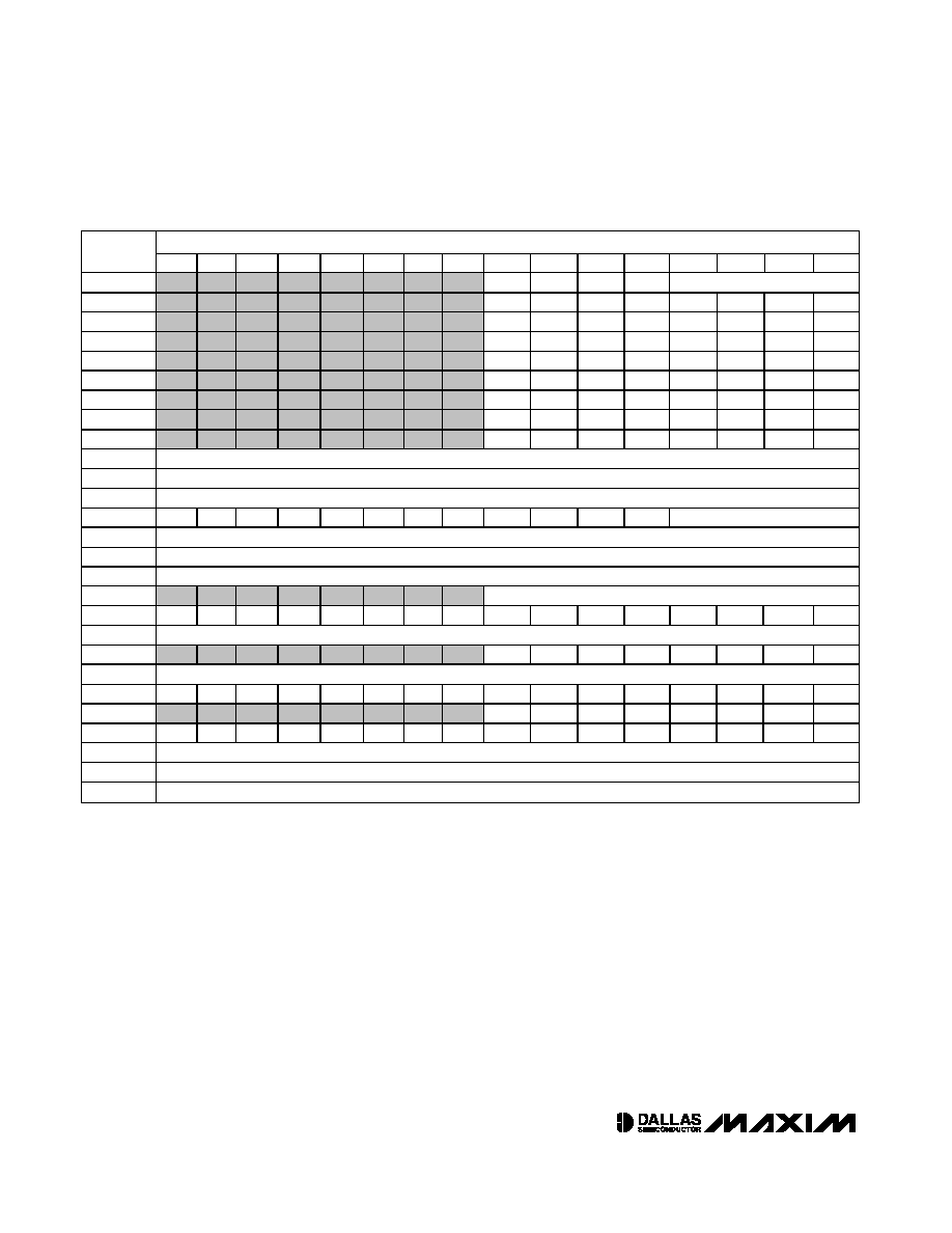
REGISTER
INDEX
AP
(8h)
A
(9h)
PFX
(Bh)
IP
(Ch)
SP
(Dh)
DPC
(Eh)
DP
(Fh)
0xh
AP
A[0]
PFX
IP
--
--
--
1xh
APC
A[1]
--
--
SP
--
--
2xh
--
A[2]
--
--
IV
--
--
3xh
--
A[3]
--
--
--
Offs
DP[0]
4xh
PSF
A[4]
--
--
--
DPC
--
5xh
IC
A[5]
--
--
--
GR
--
6xh
IMR
A[6]
--
--
LC[0]
GRL
--
7xh
--
A[7]
--
--
LC[1]
BP
DP[1]
8xh
SC
A[8]
--
--
--
GRS
--
9xh
--
A[9]
--
--
--
GRH
--
Axh
--
A[10]
--
--
--
GRXL
--
Bxh
IIR
A[11]
--
--
--
BP[offs]
--
Cxh
--
A[12]
--
--
--
--
--
Dxh
--
A[13]
--
--
--
--
--
Exh
CKCN
A[14]
--
--
--
--
--
Fxh
WDCN
A[15]
--
--
--
--
--
Note: Names that appear in italics indicate that all bits of a register are read-only. Names that appear in bold indicate that a register
is 16 bits wide. Registers in module AP are bit addressable.
MAXQ3120
High-Precision ADC
Mixed-Signal Microcontroller
14
____________________________________________________________________
Table 2. System Register Bit Functions
REGISTER BIT
REGISTER
15
14
13
12
11
10
9
8
7
6
5
4
3
2
1
0
AP
--
--
--
--
AP (4 bits)
APC
CLR
IDS
--
--
--
MOD2
MOD1
MOD0
PSF
Z
S
--
GPF1
GPF0
OV
C
E
IC
--
--
CGDS
--
--
--
INS
IGE
IMR
IMS
--
--
--
IM3
IM2
IM1
IM0
SC
TAP
--
--
--
--
ROD
PWL
--
IIR
IIS
--
--
--
II3
II2
II1
II0
CKCN
--
--
--
STOP
SWB
PMME
CD1
CD0
WDCN
POR
EWDI
WD1
WD0
WDIF
WTRF
EWT
RWT
A[0..15]
A[n] (16 bits)
PFX
PFX (16 bits)
IP
IP (16 bits)
SP
--
--
--
--
--
--
--
--
--
--
--
--
SP (4 bits)
IV
IV (16 bits)
LC[0]
LC[0] (16 bits)
LC[1]
LC[1] (16 bits)
Offs
Offs (8 bits)
DPC
--
--
--
--
--
--
--
--
--
--
--
WBS2
WBS1
WBS0
SDPS1 SDPS0
GR
GR (16 bits)
GRL
GR.7
GR.6
GR.5
GR.4
GR.3
GR.2
GR.1
GR.0
BP
BP (16 bits)
GRS
GR.7
GR.6
GR.5
GR.4
GR.3
GR.2
GR.1
GR.0
GR.15
GR.14
GR.13
GR.12
GR.11
GR.10
GR.9
GR.8
GRH
GR.15
GR.14
GR.13
GR.12
GR.11
GR.10
GR.9
GR.8
GRXL
GR.7
GR.7
GR.7
GR.7
GR.7
GR.7
GR.7
GR.7
GR.7
GR.6
GR.5
GR.4
GR.3
GR.2
GR.1
GR.0
BP[offs]
BP[offs] (16 bits)
DP[0]
DP[0] (16 bits)
DP[1]
DP[1] (16 bits)

MAXQ3120
High-Precision ADC
Mixed-Signal Microcontroller
____________________________________________________________________
15
Table 3. System Register Reset Values
REGISTER BIT
REGISTER
15
14
13
12
11
10
9
8
7
6
5
4
3
2
1
0
AP
0
0
0
0
0
0
0
0
APC
0
0
0
0
0
0
0
0
PSF
i
i
0
0
0
0
0
0
IC
0
0
0
0
0
0
0
0
IMR
0
0
0
0
0
0
0
0
SC
1
0
i
i
i
0
0
0
IIR
0
0
0
0
0
0
0
0
CKCN
1
0
0
0
0
0
0
0
WDCN
s
s
0
0
0
s
s
0
A[0..15]
i
i
i
i
i
i
i
i
i
i
i
i
i
i
i
i
PFX
0
0
0
0
0
0
0
0
0
0
0
0
0
0
0
0
IP
1
0
0
0
0
0
0
0
0
0
0
0
0
0
0
0
SP
0
0
0
0
0
0
0
0
0
0
0
0
1
1
1
1
IV
0
0
0
0
0
0
0
0
0
0
0
0
0
0
0
0
LC[0]
0
0
0
0
0
0
0
0
0
0
0
0
0
0
0
0
LC[1]
0
0
0
0
0
0
0
0
0
0
0
0
0
0
0
0
Offs
0
0
0
0
0
0
0
0
DPC
0
0
0
0
0
0
0
0
0
0
0
1
1
1
0
0
GR
0
0
0
0
0
0
0
0
0
0
0
0
0
0
0
0
GRL
0
0
0
0
0
0
0
0
BP
0
0
0
0
0
0
0
0
0
0
0
0
0
0
0
0
GRS
0
0
0
0
0
0
0
0
0
0
0
0
0
0
0
0
GRH
0
0
0
0
0
0
0
0
GRXL
0
0
0
0
0
0
0
0
0
0
0
0
0
0
0
0
BP[offs]
0
0
0
0
0
0
0
0
0
0
0
0
0
0
0
0
DP[0]
0
0
0
0
0
0
0
0
0
0
0
0
0
0
0
0
DP[1]
0
0
0
0
0
0
0
0
0
0
0
0
0
0
0
0
Note: Bits marked with an "i" have an indeterminate value upon reset. Bits marked with an "s" have special behavior upon reset.
Refer to the user's guide supplement for this device for more details.
MAXQ3120
High-Precision ADC
Mixed-Signal Microcontroller
16
____________________________________________________________________
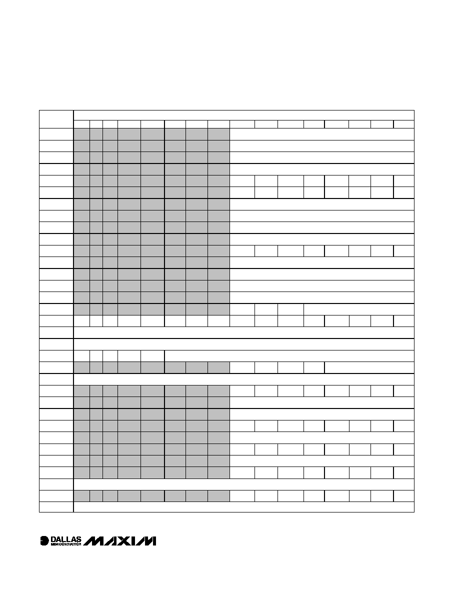
Table 4. Peripheral Register Map
REGISTER
INDEX
M0
(0h)
M1
(1h)
M2
(2h)
M3
(3h)
M4
(4h)
M5
(5h)
00h
PO0
T0CN
T1CN
MCNT
--
--
01h
PO1
T0L
T1L
MA
--
--
02h
PO2
T0H
T1H
MB
--
--
03h
PO3
SCON0
T2CNA
MC2
--
--
04h
--
SBUF0
T2H
MC1
--
--
05h
--
SCON1
T2RH
MC0
--
--
06h
EIF0
SBUF1
T2CH
MC1R
--
--
07h
EIE0
--
IRCN
MC0R
--
--
08h
PI0
--
T1CL
ADCN
--
--
09h
PI1
SMD0
T1CH
PHC
--
--
0Ah
PI2
PR0
T1MD
AD0
--
--
0Bh
PI3
SMD1
T2CNB
AD1
--
--
0Ch
EIES0
PR1
T2V
ATRM
--
--
0Dh
--
--
T2R
LCRA
--
--
0Eh
--
--
T2C
LCFG
--
--
0Fh
--
--
T2CFG
--
--
--
10h
PD0
--
--
LCD0
--
--
11h
PD1
--
--
LCD1
--
--
12h
PD2
--
--
LCD2
--
--
13h
PD3
--
--
LCD3
--
--
14h
--
--
--
LCD4
--
--
15h
--
--
--
LCD5
--
--
16h
--
--
--
LCD6
--
--
17h
--
--
--
LCD7
--
--
18h
RTRM
--
--
LCD8
--
--
19h
RCNT
--
--
LCD9
--
--
1Ah
RTSS
--
--
LCD10
--
--
1Bh
RTSH
ICDF
--
LCD11
--
--
1Ch
RTSL
--
--
LCD12
--
--
1Dh
RSSA
--
--
LCD13
--
--
1Eh
RASH
--
--
--
--
--
1Fh
RASL
--
--
--
--
--
Note: Names that appear in italics indicate that all bits of a register are read-only. Names that appear in bold indicate that a register
is 16 bits wide. Registers in module AP are bit addressable.
MAXQ3120
High-Precision ADC
Mixed-Signal Microcontroller
____________________________________________________________________
17
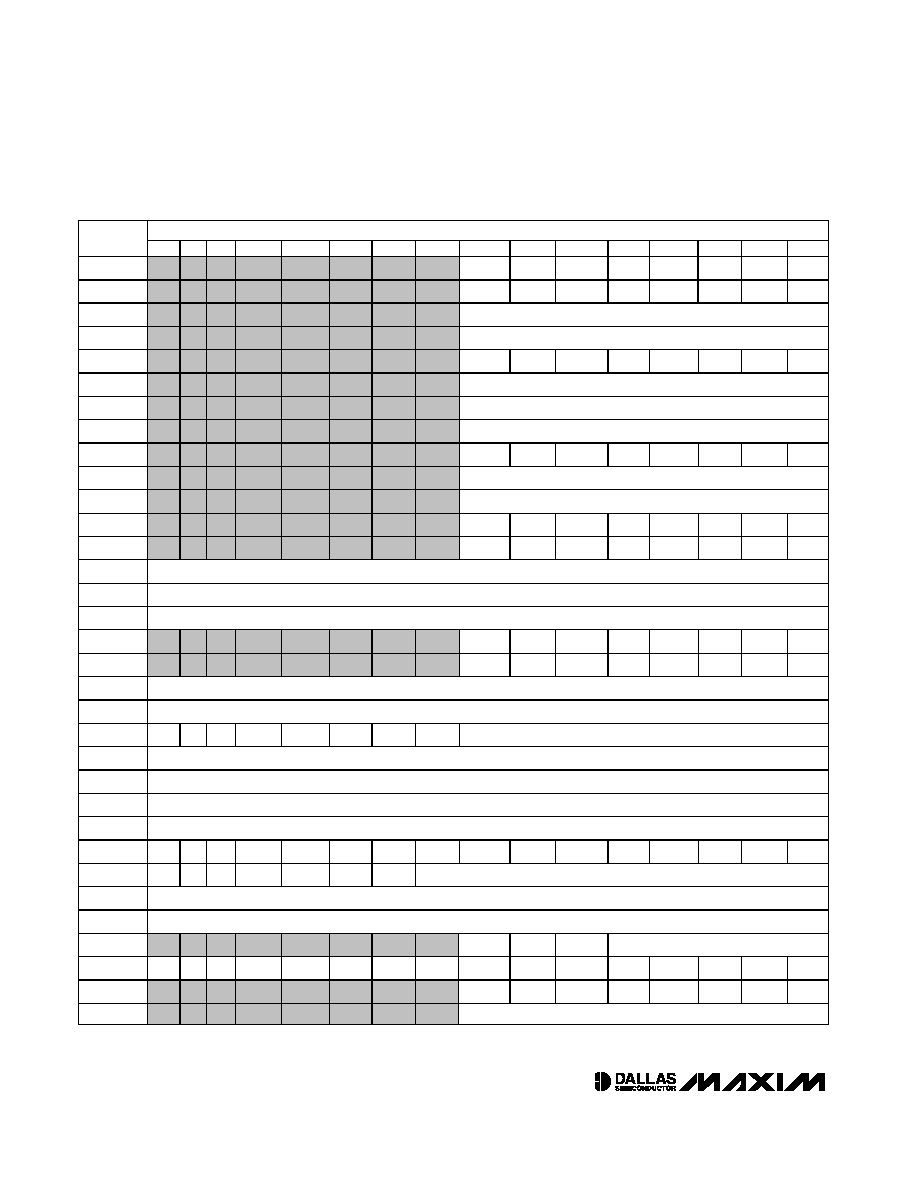
Table 5. Peripheral Register Bit Functions
REGISTER BIT
REGISTER
15
14
13
12
11
10
9
8
7
6
5
4
3
2
1
0
PO0
PO0 (8 bits)
PO1
PO1 (8 bits)
PO2
PO2 (8 bits)
PO3
PO3 (8 bits)
EIF0
--
--
--
--
--
IE2
IE1
IE0
EIE0
--
--
--
--
--
EX2
EX1
EX0
PI0
PI0 (8 bits)
PI1
PI1 (8 bits)
PI2
PI2 (8 bits)
PI3
PI3 (8 bits)
EIES0
--
--
--
--
--
IT2
IT1
IT0
PD0
PD0 (8 bits)
PD1
PD1 (8 bits)
PD2
PD2 (8 bits)
PD3
PD3 (8 bits)
RTRM
--
--
TSGN
TRM (5 bits)
RCNT
WE
--
--
--
--
--
FT
SQE
ALSF
ALDF
RDYE
RDY
BUSY
ASE
ADE
RTCE
RTSH
RTSH (16 bits)
RTSL
RTSL (16 bits)
RSSA
--
--
--
--
--
RSSA (11 bits)
RASH
--
--
--
--
RASH (4 bits)
RASL
RASL (16 bits)
T0CN
ET0
T0M
TF0
TR0
GATE
C/T
M1
M0
T0L
T0L (8 bits)
T0H
T0H (8 bits)
SCON0
SM0/FE
SM1
SM2
REN
TB8
RB8
TI
RI
SBUF0
SBUF0 (8 bits)
SCON1
SM0/FE
SM1
SM2
REN
TB8
RB8
TI
RI
SBUF1
SBUF1 (8 bits)
SMD0
EPWM
OFS
--
--
--
ESI
SMOD
FEDE
PR0
PR0 (16 bits)
SMD1
--
--
--
--
--
ESI
SMOD
FEDE
PR1
PR1 (16 bits)
MAXQ3120
High-Precision ADC
Mixed-Signal Microcontroller
18
____________________________________________________________________
Table 5. Peripheral Register Bit Functions (continued)
REGISTER BIT
REGISTER
15
14
13
12
11
10
9
8
7
6
5
4
3
2
1
0
ICDF
--
--
--
--
PSS1
PSS0
SPE
--
T1CN
TF1
EXF1
T1OE
DCEN
EXEN1
TR1
C/T1
CPRL1
T1L
T1L (8 bits)
T1H
T1H (8 bits)
T2CNA
ET2
T2OE0
T2POL0
TR2L
TR2
CPRL2
SS2
G2EN
T2H
T2V[15:8] (8 bits)
T2RH
T2R[15:8] (8 bits)
T2CH
T2C[15:8] (8 bits)
IRCN
--
--
--
--
--
IREN
IRTX
IRBB
T1CL
T1CL (8 bits)
T1CH
T1CH (8 bits)
T1MD
--
--
--
--
--
--
ET1
T1M
T2CNB
ET2L
T2OE1
T2POL1
--
TF2
TCC2
TF2L
TC2L
T2V
T2V (16 bits)
T2R
T2R (16 bits)
T2C
T2C (16 bits)
T2CFG
T2CI
DIV2
DIV1
DIV0
T2MD
CCF1
CCF0
C/T2
MCNT
OF
MCW
CLD
SQU
OPCS
MSUB
MMAC
SUS
MA
MA (16 bits)
MB
MB (16 bits)
MC2
--
--
--
--
--
--
--
--
MC2 (8 bits)
MC1
MC1 (16 bits)
MC0
MC0 (16 bits)
MC1R
MC1R (16 bits)
MC0R
MC0R (16 bits)
ADCN
G3
G2
G1
G0
--
APD2
APD1
APD0
UFF
EDBI
FLU1
FLU0
FOV1
FOV0
ABF1
ABF0
PHC
ZPS
--
--
--
--
--
--
PH (9 bits)
AD0
AD0 (16 bits)
AD1
AD1 (16 bits)
ATRM
--
--
--
ABGT (5 bits)
LCRA
--
--
--
DUTY1
DUTY0
FRM3
FRM2
FRM1
FRM0
LCCS
LRIG
--
LRA3
LRA2
LRA1
LRA0
LCFG
PCF3
PCF2
PCF1
PCF0
--
--
OPM
DPE
LCD[0..13]
LCD[n] (8 bits)

MAXQ3120
High-Precision ADC
Mixed-Signal Microcontroller
____________________________________________________________________
19
Table 6. Peripheral Register Bit Reset Values
REGISTER BIT
REGISTER
15
14
13
12
11
10
9
8
7
6
5
4
3
2
1
0
PO0
1
1
1
1
1
1
1
1
PO1
1
1
1
1
1
1
1
1
PO2
1
1
1
1
1
1
1
1
PO3
1
1
1
1
1
1
1
1
EIF0
0
0
0
0
0
0
0
0
EIE0
0
0
0
0
0
0
0
0
PI0
s
s
s
s
s
s
s
s
PI1
s
s
s
s
s
s
s
s
PI2
s
s
s
s
s
s
s
s
PI3
s
s
s
s
s
s
s
s
EIES0
0
0
0
0
0
0
0
0
PD0
0
0
0
0
0
0
0
0
PD1
0
0
0
0
0
0
0
0
PD2
0
0
0
0
0
0
0
0
PD3
0
0
0
0
0
0
0
0
RTRM
0
0
s
s
s
s
s
s
RCNT
0
0
0
0
0
0
0
0
0
0
0
0
1
0
0
s
RTSS
s
s
s
s
s
s
s
s
RTSH
s
s
s
s
s
s
s
s
s
s
s
s
s
s
s
s
RTSL
s
s
s
s
s
s
s
s
s
s
s
s
s
s
s
s
RSSA
0
0
0
0
0
s
s
s
s
s
s
s
s
s
s
s
RASH
0
0
0
0
s
s
s
s
RASL
s
s
s
s
s
s
s
s
s
s
s
s
s
s
s
s
T0CN
0
0
0
0
0
0
0
0
T0L
0
0
0
0
0
0
0
0
T0H
0
0
0
0
0
0
0
0
SCON0
0
0
0
0
0
0
0
0
SBUF0
0
0
0
0
0
0
0
0
SCON1
0
0
0
0
0
0
0
0
SBUF1
0
0
0
0
0
0
0
0
SMD0
0
0
0
0
0
0
0
0
PR0
0
0
0
0
0
0
0
0
0
0
0
0
0
0
0
0
SMD1
0
0
0
0
0
0
0
0
PR1
0
0
0
0
0
0
0
0
0
0
0
0
0
0
0
0
ICDF
0
0
0
0
0
0
0
0
T1CN
0
0
0
0
0
0
0
0
T1L
0
0
0
0
0
0
0
0

MAXQ3120
High-Precision ADC
Mixed-Signal Microcontroller
20
____________________________________________________________________
Table 6. Peripheral Register Bit Reset Values (continued)
REGISTER BIT
REGISTER
15
14
13
12
11
10
9
8
7
6
5
4
3
2
1
0
T1H
0
0
0
0
0
0
0
0
T2CNA
0
0
0
0
0
0
0
0
T2H
0
0
0
0
0
0
0
0
T2RH
0
0
0
0
0
0
0
0
T2CH
0
0
0
0
0
0
0
0
IRCN
0
0
0
0
0
0
0
0
T1CL
0
0
0
0
0
0
0
0
T1CH
0
0
0
0
0
0
0
0
T1MD
0
0
0
0
0
0
0
0
T2CNB
0
0
0
0
0
0
0
0
T2V
0
0
0
0
0
0
0
0
0
0
0
0
0
0
0
0
T2R
0
0
0
0
0
0
0
0
0
0
0
0
0
0
0
0
T2C
0
0
0
0
0
0
0
0
0
0
0
0
0
0
0
0
T2CFG
0
0
0
0
0
0
0
0
MCNT
0
0
0
0
0
0
0
0
MA
0
0
0
0
0
0
0
0
0
0
0
0
0
0
0
0
MB
0
0
0
0
0
0
0
0
0
0
0
0
0
0
0
0
MC2
0
0
0
0
0
0
0
0
0
0
0
0
0
0
0
0
MC1
0
0
0
0
0
0
0
0
0
0
0
0
0
0
0
0
MC0
0
0
0
0
0
0
0
0
0
0
0
0
0
0
0
0
MC1R
0
0
0
0
0
0
0
0
0
0
0
0
0
0
0
0
MC0R
0
0
0
0
0
0
0
0
0
0
0
0
0
0
0
0
ADCN
s
s
s
s
0
s
s
s
0
0
0
0
0
0
0
0
PHC
s
0
0
0
0
0
0
s
s
s
s
s
s
s
s
s
AD0
i
i
i
i
i
i
i
i
i
i
i
i
i
i
i
i
AD1
i
i
i
i
i
i
i
i
i
i
i
i
i
i
i
i
ATRM
0
0
0
s
s
s
s
s
LCRA
0
0
0
0
0
0
0
0
0
0
0
0
0
0
0
0
LCFG
0
0
0
0
0
0
0
0
LCD[0..13]
0
0
0
0
0
0
0
0
Note: Bits marked with an "i" have an indeterminate value upon reset. Bits marked with an "s" have special behavior upon reset.
Refer to the user's guide supplement for this device for more details.
MAXQ3120
High-Precision ADC
Mixed-Signal Microcontroller
____________________________________________________________________
21
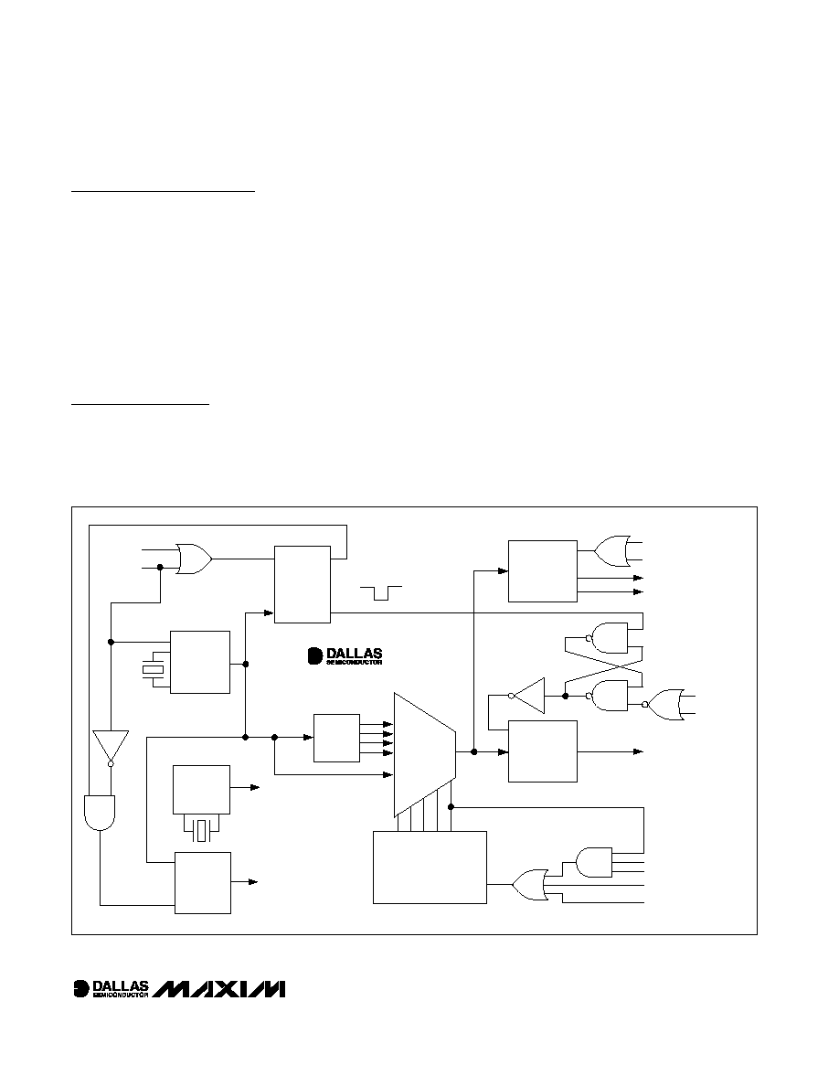
System Timing
The MAXQ3120 generates its internal system clock
from an external high-frequency crystal. Because the
MAXQ3120 includes internal capacitors for this pur-
pose, no external capacitors are required to use the
high-frequency crystal. The MAXQ3120 should not be
driven directly by an external clock source.
A crystal warmup counter enhances operational relia-
bility. Each time the external crystal oscillation must
restart, such as after exiting stop mode, the device initi-
ates a crystal warmup period of 65,536 oscillations.
This allows time for the crystal amplitude and frequency
to stabilize before using it as a clock source.
Power Management
Advanced power-management features minimize power
consumption by dynamically matching the processing
speed of the device to the required performance level.
This means device operation can be slowed and power
consumption minimized during periods of reduced
activity. When more processing power is required, the
microcontroller can increase its operating frequency.
Software-selectable clock-divide operations allow flexi-
bility, selecting whether a system clock cycle is 1, 2, 4,
or 8 oscillator cycles. By performing this function in soft-
ware, a lower power state can be entered without the
cost of additional hardware.
For extremely power-sensitive applications, two addi-
tional low-power modes are available.
∑ Divide-by-256 power-management mode (PMM)
(PMME = 1, CD1:0 = 00b)
∑ Stop mode (STOP = 1)
In PMM, one system clock is 256 oscillator cycles, signifi-
cantly reducing power consumption while the microcon-
troller functions at reduced speed. The optional
switchback feature allows enabled interrupt sources,
such as the external interrupts and USARTs, to cause the
processor to quickly exit PMM mode and return to a
faster internal clock rate.
Figure 2. Clock Sources
MAXQ3120
GLITCH-FREE
MUX
DIV 1
DIV 2
DIV 4
DIV 8
PWM
CLOCK
DIVIDER
SELECTOR
DEFAULT
WATCHDOG
TIMER
RESET DOG
RWT
RESET
POWER-ON
RESET
STOP
STOP
POWER-ON
RESET
SWB
INTERRUPT/SERIAL PORT
RESET
STOP
POWER MONITOR
REAL-TIME CLOCK
LCD CONTROLLER
WATCHDOG RESET
CLOCK
GENERATION
SYSTEM CLOCK
ENABLE
WATCHDOG INTERRUPT
32kHz
CRYSTAL
CRYSTAL
MONITOR
ENABLE
INPUT
HF
CRYSTAL
CRYSTAL KILL
XDOG
STARTUP
TIMER
CLK INPUT
RESET
XDOG COUNT
XDOG DONE

MAXQ3120
Power consumption reaches its minimum in stop mode.
In this mode, the external high-frequency oscillator,
system clock, and all code execution is halted. Stop
mode is exited when an enabled external interrupt pin
is triggered, an external reset signal is applied to the
RESET pin, or the RTC time-of-day alarm is activated.
The 32kHz clock continues running during stop mode,
enabling the following peripherals to keep running dur-
ing stop mode.
∑ The RTC always continues running during stop
mode.
∑ The LCD controller continues running during stop
mode if it is running from the 32kHz clock (LCCS = 0).
Interrupts
Multiple reset sources are available for quick response
to internal and external events. The MAXQ architecture
uses a single interrupt vector (IV), single interrupt-ser-
vice routine (ISR) design. For maximum flexibility, inter-
rupts can be enabled globally, individually, or by
module. When an interrupt condition occurs, its individ-
ual flag is set, even if the interrupt source is disabled at
the local, module, or global level. Interrupt flags must
be cleared within the user-interrupt routine to avoid
repeated interrupts from the same source. Application
software must ensure a delay between the write to the
flag and the RETI instruction to allow time for the inter-
rupt hardware to remove the internal interrupt condition.
Asynchronous interrupt flags require a one-instruction
delay and synchronous interrupt flags require a two-
instruction delay.
When an enabled interrupt is detected, software jumps
to a user-programmable interrupt vector location. The
IV register defaults to 0000h on reset or power-up, so if
it is not changed to a different address, the user pro-
gram must determine whether a jump to 0000h came
from a reset or interrupt source.
Once software control has been transferred to the ISR,
the interrupt identification register (IIR) can determine if
a system register or peripheral register was the source
of the interrupt. The specified module can then be inter-
rogated for the specific interrupt source and software
can take appropriate action. Because the interrupts are
evaluated by user software, the user can define a
unique interrupt priority scheme for each application.
The following interrupt sources are available.
∑ Watchdog Interrupt
∑ External Interrupts 0 to 2
∑ RTC Time-of-Day and Subsecond Alarms
∑ Serial Port 0 Receive and Transmit Interrupts
∑ Serial Port 1 Receive and Transmit Interrupts
∑ Timer 0 Overflow Interrupt
∑ Timer 1 Overflow and External Trigger Interrupts
∑ Timer 2 Low Compare, Low Overflow, Capture/
Compare, and Overflow Interrupts
Reset Sources
Several reset sources are provided for microcontroller
control. Although code execution is halted in the reset
state, the high-frequency oscillator and the 32kHz oscilla-
tor continue to oscillate. Internal resets such as the
power-on and watchdog resets assert the RESET pin low.
Power-On Reset
An internal power-on reset circuit enhances system reli-
ability. This circuit forces the device to perform a
power-on reset whenever a rising voltage on DV
DD
climbs above the V
RST
level. At this point, the following
events occur:
∑ All registers and circuits enter their reset state
(except for the RTC, if it is battery-backed)
∑ The POR flag (WDCN.7) is set to indicate the source
of the reset
∑ Code execution begins at location 8000h
Watchdog Timer Reset
The watchdog timer functions are described in the
MAXQ Family User's Guide. Execution resumes at loca-
tion 8000h following a watchdog timer reset.
External System Reset
Asserting the external RESET pin low causes the
device to enter the reset state. The external reset func-
tions as described in the MAXQ Family User's Guide.
Execution resumes at location 8000h after the RESET
pin is released.
I/O Ports
The microcontroller uses the Type C and Type D bidi-
rectional I/O ports described in the MAXQ Family
User's Guide. The use of two port types allows for maxi-
mum flexibility when interfacing to external peripherals.
Each port has eight independent, general-purpose I/O
pins and three configure/control registers. Many pins
support alternate functions such as timers or interrupts,
which are enabled, controlled, and monitored by dedi-
cated peripheral registers. Using the alternate function
automatically converts the pin to that function.
High-Precision ADC
Mixed-Signal Microcontroller
22
____________________________________________________________________

Type C port pins have Schmitt Trigger receivers and
full CMOS output drivers, and can support alternate
functions. The pin is either tri-stated or a weak pullup
when defined as an input, dependent on the state of
the corresponding bit in the output register.
Type D port pins have Schmitt Trigger receivers and
full CMOS output drivers, and can support alternate
functions. The pin is either tri-stated or a weak pullup
when defined as an input, dependent on the state of
the corresponding bit in the output register. All Type D
pins also have interrupt capability.
High-Speed Hardware Multiplier
The hardware multiplier module performs high-speed
multiply, square, and accumulate operations, and can
complete a 16-bit x 16-bit multiply-and-accumulate
operation in a single cycle. The hardware multiplier
consists of two 16-bit parallel-load operand registers
(MA, MB), a 40-bit accumulator that is formed by three
16-bit parallel registers (MC2, MC1, and MC0), and a
status/control register (MCNT). Loading the registers
can automatically initiate the operation, saving time on
repetitive calculations. The accumulate function of the
hardware multiplier is an essential element of digital fil-
tering, signal processing, and proportional/integral/
derivative (PID) algorithm-based control systems.
The hardware multiplier module supports the following
operations:
∑ Multiply unsigned (16 bit x 16 bit)
∑ Multiply signed (16 bit x 16 bit)
∑ Multiply-accumulate unsigned (16 bit x 16 bit)
∑ Multiply-accumulate signed (16 bit x 16 bit)
∑ Square unsigned (16 bit)
∑ Square signed (16 bit)
∑ Square-accumulate unsigned (16 bit)
∑ Square-accumulate signed (16 bit)
MAXQ3120
High-Precision ADC
Mixed-Signal Microcontroller
____________________________________________________________________
23
MAXQ3120
PD.x
SF DIRECTION
SF ENABLE
MUX
MUX
PO.x
V
DDIO
SF OUTPUT
V
DDIO
WEAK
I/O PAD
PORT PIN
INTERRUPT
FLAG
FLAG
PI.x OR SF INPUT
EIES.x
TYPE D PORT ONLY
DETECT
CIRCUIT
Figure 3. Type C/D Port Pin Schematic

MAXQ3120
Real-Time Clock
A binary real-time clock keeps the time of day in
absolute seconds with 1/256-second resolution. The
32-bit second counter can count up to approximately
136 years and be translated to calendar format by the
application software. A time-of-day alarm and indepen-
dent subsecond alarm can cause an interrupt, or wake
the device from stop mode.
The independent subsecond alarm runs from the same
RTC, and allows the application to perform periodic
interrupts up to 8 seconds with a granularity of approxi-
mately 3.9ms. This creates an additional timer that can
be used to measure long periods without performance
degradations. Traditionally, long time periods have
been measured using multiple interrupts from shorter
programmable timers. Each timer interrupt required
servicing, with each accompanying interruption slowing
system operation. By using the RTC subsecond timer
as a long-period timer, only one interrupt is needed,
eliminating the performance hit associated with using a
shorter timer.
An internal crystal oscillator clocks the RTC using inte-
grated 6pF load capacitors, and gives the best perfor-
mance when mated with a 32.768kHz crystal rated for a
6pF load. No external load capacitors are required.
Higher accuracy can be obtained by using the digital
RTC trim function. The frequency accuracy of a crystal-
based oscillator circuit is dependent upon crystal accu-
racy, the match between the crystal and the oscillator
capacitor load, ambient temperature, etc.
Programmable Timers
The MAXQ3120 incorporates one instance each of the
timer 0, timer 1, and timer 2 peripherals. These timers
can be used in counter/timer/capture/compare/PWM
functions, allowing precise control of internal and exter-
nal events. Timer 2 supports optional single-shot, exter-
nal gating, and polarity control options as well as
carrier generation support for infrared transmit/receive
functions using serial port 0.
Timer 0
The timer 0 peripheral includes the following:
∑ 8-bit autoreload timer/counter
∑ 13-bit or 16-bit timer/counter
∑ Dual 8-bit timer/counter
∑ External pulse counter
Timer 1
The timer 1 peripheral includes the following:
∑ 16-bit autoreload timer/counter
∑ 16-bit capture
∑ 16-bit counter
∑ Clock generation output
Timer 2
The timer 2 peripheral includes the following:
∑ 16-bit autoreload timer/counter
∑ 16-bit capture
∑ 16-bit counter
∑ 8-bit capture and 8-bit timer
∑ 8-bit counter and 8-bit timer
∑ Infrared carrier generation support
Watchdog Timer
An internal watchdog timer greatly increases system
reliability. The timer resets the processor if software
execution is disturbed. The watchdog timer is a free-
running counter designed to be periodically reset by
the application software. If software is operating cor-
rectly, the counter is periodically reset and never
reaches its maximum count. However, if software oper-
ation is interrupted, the timer does not reset, triggering
a system reset and optionally a watchdog timer inter-
rupt. This protects the system against electrical noise
or electrostatic discharge (ESD) upsets that could
cause uncontrolled processor operation. The internal
watchdog timer is an upgrade to older designs with
external watchdog devices, reducing system cost and
simultaneously increasing reliability.
The watchdog timer is controlled through bits in the
WDCN register. Its timeout period can be set to one of
four programmable intervals ranging from 2
12
to 2
21
system clocks in its default mode, allowing flexibility to
support different types of applications. The interrupt
occurs 512 system clocks before the reset, allowing the
system to execute an interrupt and place the system in
a known, safe state before the device performs a total
system reset. At 8MHz, watchdog timeout periods can
be programmed from 512µs to 61.7s, depending on the
system clock mode.
High-Precision ADC
Mixed-Signal Microcontroller
24
____________________________________________________________________

In-Circuit Debug
Embedded debugging capability is available through
the JTAG-compatible TAP. Embedded debug hardware
and embedded ROM firmware provide in-circuit
debugging capability to the user application, eliminat-
ing the need for an expensive in-circuit emulator.
Figure 4 shows a block diagram of the in-circuit debug-
ger. The in-circuit debug features include:
∑ Hardware debug engine
∑ Set of registers able to set breakpoints on register,
code, or data accesses
∑ Set of debug service routines stored in the utility
ROM
The embedded hardware debug engine is an indepen-
dent hardware block in the microcontroller. The debug
engine can monitor internal activities and interact with
selected internal registers while the CPU is executing
user code. Collectively, the hardware and software fea-
tures allow two basic modes of in-circuit debugging:
∑ Background mode allows the host to configure and set
up the in-circuit debugger while the CPU continues to
execute the application software at full speed. Debug
mode can be invoked from background mode.
∑ Debug mode allows the debug engine to take control
of the CPU, providing read/write access to internal reg-
isters and memory, and single-step trace operation.
Serial Peripherals
The MAXQ3120 incorporates two 8051-style universal
synchronous/asynchronous receiver/transmitters. The
USARTs allow the device to conveniently communicate
with other RS-232 interface-enabled devices, as well as
PCs and serial modems when paired with an external
RS-232 line driver/receiver. The dual independent
USARTs can communicate simultaneously at different
baud rates with two separate peripherals. The USART
can detect framing errors and indicate the condition
through a user-accessible software bit.
The time base of the serial ports is derived from either a
division of the system clock or the dedicated baud
clock generator. The following table summarizes the
operating characteristics as well as the maximum baud
rate of each mode.
Serial port 0 contains additional functionality to support
low-speed infrared transmission in combination with the
PWM function of timer 2. When enabled in this mode,
the serial port automatically outputs a waveform gener-
ated by combining the normal serial port output wave-
form with the PWM carrier waveform output by timer 2,
using a logical OR or logical NOR function. The output
of serial port 0 in this mode can be used to drive an
infrared LED to communicate using a fixed-frequency
carrier modulated signal. Depending on the drive
strength required, the output may require a buffer when
used for this purpose.
MAXQ3120
High-Precision ADC
Mixed-Signal Microcontroller
____________________________________________________________________
25
MODE
TYPE
START BITS
DATA BITS
STOP BIT
MAX BAUD RATE AT 8MHz
Mode 0
Synchronous
--
8
--
2Mbps
Mode 1
Asynchronous
1
8
1
250kbps
Mode 2
Asynchronous
1
8 + 1
1
250kbps
Mode 3
Asynchronous
1
8 + 1
1
250kbps
Figure 4. In-Circuit Debugger
TAP
CONTROLLER
CPU
DEBUG
ENGINE
DEBUG
SERVICE
ROUTINES
(UTILITY ROM)
TMS
TCK
TDI
TDO
CONTROL
BREAKPOINT
ADDRESS
DATA
MAXQ3120
MAXQ3120
LCD Driver
The MAXQ3120 microcontroller incorporates an LCD
driver that interfaces to common low-voltage displays.
By incorporating the LCD driver into the microcon-
troller, the design requires only an LCD glass rather
than a considerably more expensive LCD module.
Every character in an LCD glass is composed of one or
more segments, each of which is activated by selecting
the appropriate segment and common signal. The
microcontroller can drive up to 112 LCD glass seg-
ments by multiplexing combinations of 28 segment
(SEG0≠SEG27) outputs and four common-signal out-
puts (COM0≠COM3). Eight of the segment outputs can
also be used as general-purpose port pins, if they are
not needed to drive the LCD.
The segments are easily addressed by writing to dedi-
cated display memory. Once the LCD driver settings
and display memory have been initialized, the 14-byte
display memory is periodically scanned, and the seg-
ment and common signals are generated automatically
at the selected display frequency. No additional proces-
sor overhead is required while the LCD driver is running.
Unused display memory can be used for general-pur-
pose storage.
The design is further simplified and cost-reduced by
the inclusion of software-adjustable internal voltage-
dividers to control display contrast. If desired, contrast
can also be controlled by an external resistance. The
features of the LCD driver include the following:
∑ Automatic LCD segment and common-drive signal
generation
∑ Four display modes supported:
Static (COM0)
1/2 duty multiplexed with 1/2 bias voltages
(COM0, COM1)
1/3 duty multiplexed with 1/3 bias voltages
(COM0, COM1, COM2)
1/4 duty multiplexed with 1/3 bias voltages
(COM0, COM1, COM2, COM3)
∑ Up to 28 segment outputs and four common-signal
outputs
∑ 14 bytes (112 bits) of display memory
∑ Adjustable frame frequency
∑ Internal voltage-divider resistors eliminate require-
ment for external components
∑ Internal adjustable resistor allows contrast adjust-
ment without external components
∑ Flexibility to use external resistors to adjust drive
voltages and current capacity
A simple LCD-segmented glass interface example
demonstrates the minimal hardware required to inter-
face to a MAXQ3120 microcontroller. A two-character
LCD is controlled, with each character containing
seven segments plus decimal point. The LCD driver is
configured for 1/2 duty cycle operation, meaning the
active segment is controlled using a combination of
segment signals, and COM0 or COM1 signals are used
to select the active display.
High-Precision ADC
Mixed-Signal Microcontroller
26
____________________________________________________________________
Figure 5. Two-Character, 1/2 Duty, LCD Interface Example
SEG0
SEG1
SEG2
SEG3
COM0
SEG0:7
CONNECTED TO DARK GREY SEGMENTS
COM1
CONNECTED TO LIGHT GREY SEGMENTS
SEG4
SEG5
SEG6
SEG7
MAXQ3120

Analog Front-End
The MAXQ3120 microcontroller incorporates an analog
front-end for dedicated analog-to-digital conversion.
This peripheral converts and digitally filters two differ-
ential signal channels with no CPU overhead.
The two conversion channels operate completely in
parallel, running at the same sample rate whether one
channel or both channels are enabled. If one or both
channels are not in use, they may be powered down to
conserve supply current.
The two input signals for each channel form a true differ-
ential pair. Each of the two signals (AN0+ and AN0- for
channel 0, AN1+ and AN1- for channel 1) can vary
across the entire +1V to -1V analog input range, without
regard to the level of the other signal in the pair. The ini-
tial stage for each channel is a programmable gain
function (1x, 16x) that can be set by software indepen-
dently for each channel. Next, a second-order sigma-
delta modulator samples each input signal.
When using both channels to measure the same signal
(as is the case when measuring voltage and current for
power calculations), a phase-correction buffer is pro-
vided to compensate for any phase shift between the
two channels caused by external circuitry. The phase-
correction buffer operates digitally on the output bit
stream of one of the two channels and can delay either
channel's bit stream with respect to the other channel's
bit stream by up to 140 bits.
Next, the bit streams for the two channels travel through
two digital sinc
3
lowpass filters, which convert the bit
streams to 16-bit PCM values for additional processing.
MAXQ3120
High-Precision ADC
Mixed-Signal Microcontroller
____________________________________________________________________
27
Figure 6. Analog Front-End Block Diagram
CHANNEL 0
PROGRAMMABLE
GAIN
(1x, 16x)
AN0+
AN0-
AN1+
AN0-
CHANNEL1
PROGRAMMABLE
GAIN
(1x, 16x)
CHANNEL 0
SIGMA-DELTA
MODULATOR
CHANNEL 1
SIGMA-DELTA
MODULATOR
PHASE
CORRECTION
AD0
AD1
CHANNEL 0
SINC
3
FILTER
CHANNEL 1
SINC
3
FILTER

MAXQ3120
Applications Information
The low-power, high-performance RISC architecture of
the MAXQ3120 makes it an excellent fit for many
portable or battery-powered applications that require
cost-effective computing. The high-throughput core is
complemented by a dual-differential channel, 16-bit
sigma-delta ADC, and 16-bit hardware multiplier-accu-
mulator, allowing the implementation of sophisticated
computational algorithms. Applications benefit from a
wide range of peripheral interfaces, allowing the micro-
controller to communicate with many external devices.
With integrated LCD support of up to 112 segments (4 x
28), applications can support complex user interfaces.
Displays are driven directly with no additional external
hardware required. Contrast can be adjusted using a
built-in, adjustable resistor. The simplified architecture
reduces component count and board space, critical
factors in the design of portable systems.
The MAXQ3120 is ideally suited for single-phase elec-
tricity metering applications as well as other applica-
tions that require high-precision analog-to-digital
conversion and signal processing.
Additional Documentation
Designers must have four documents to fully use all the
features of this device. This data sheet contains pin
descriptions, feature overviews, and electrical specifi-
cations. Errata sheets contain deviations from pub-
lished specifications. The user's guides offer detailed
information about programming, device features, and
operation. The following documents can be down-
loaded from www.maxim-ic.com/microcontrollers.
∑ The MAXQ3120 data sheet, which contains electri-
cal/timing specifications and pin descriptions, avail-
able at www.maxim-ic.com/MAXQ3120.
∑ The MAXQ3120 errata sheet, available at
www.maxim-ic.com/errata.
∑ The MAXQ Family User's Guide, which contains
detailed information on core features and operation,
including programming, avaliable at www.maxim-
ic.com/MAXQUG.
∑ The MAXQ Family User's Guide: MAXQ3120
Supplement, which contains detailed information on
features specific to the MAXQ3120, available at
www.maxim-ic.com/MAXQ3120UG.
Development and Technical Support
A variety of highly versatile, affordably priced develop-
ment tools for this microcontroller are available from
Maxim/Dallas Semiconductor and third-party suppliers,
including:
∑ Compilers
∑ In-circuit emulators
∑ Integrated development environments (IDEs)
∑ JTAG-to-serial converters for programming and
debugging
A partial list of development tool vendors can be found
on our website at www.maxim-ic.com/microcontrollers.
Technical support is available through email at
maxq.support@dalsemi.com.
Definitions
Offset Error
For an ideal converter, the first transition occurs at 0.5
LSB above zero. Offset error is the amount of deviation
between the measured first transition point and the
ideal point.
Gain Error
With a full-scale analog voltage applied to the ADC
(resulting in all ones in the digital code), gain error is
defined as the amount of deviation between the ideal
transfer function and the measured transfer function
(with the offset error removed). Gain error is usually
expressed in LSB or as a percentage of full-scale
range (%FSR).
Power-Supply Rejection Ratio
Power-supply rejection ratio (PSRR) is the ratio of
changes in the power supply (V) to changes in the con-
verter output (V). It is typically measured in decibels.
High-Precision ADC
Mixed-Signal Microcontroller
28
____________________________________________________________________

Appendix A: Applying a Lowpass
Filter (LPF) for Application-
Optimized ADC Performance
The MAXQ3120 gives a user application program direct
access to the ADC data stream right after its sinc3 fil-
ters. This unique feature permits the MAXQ3120 to be
optimized for its target applications. With the device's
8MIPS processing power and the 1-cycle MAC, a linear
FIR filter can be easily computed in the user application
program. This section provides a simple LP FIR filter to
improve the SNR and THD performance of the
MAXQ3120 for the power-metering application.
Filter Specifications and Coefficients
Input signal frequency (f
IN
) = 60Hz
Sampling frequency (f
S
) = 20833Hz
Window = hamming
Cutoff frequency (attenuates after 7th harmonic) = 0.06
= 625Hz
Cutoff frequency (for 21st harmonic) = 0.18
= 1875Hz
Transition width = 0.35
= 3646Hz
Filter length = 23
MAXQ3120
High-Precision ADC
Mixed-Signal Microcontroller
____________________________________________________________________
29
FILTER_COEFFICIENT_0
-19
FILTER_COEFFICIENT_12
21893
FILTER_COEFFICIENT_1
-288
FILTER_COEFFICIENT_13
17547
FILTER_COEFFICIENT_2
-786
FILTER_COEFFICIENT_14
11739
FILTER_COEFFICIENT_3
-1402
FILTER_COEFFICIENT_15
6018
FILTER_COEFFICIENT_4
-1670
FILTER_COEFFICIENT_16
1627
FILTER_COEFFICIENT_5
-876
FILTER_COEFFICIENT_17
-876
FILTER_COEFFICIENT_6
1627
FILTER_COEFFICIENT_18
-1670
FILTER_COEFFICIENT_7
6018
FILTER_COEFFICIENT_19
-1402
FILTER_COEFFICIENT_8
11739
FILTER_COEFFICIENT_20
-786
FILTER_COEFFICIENT_9
17547
FILTER_COEFFICIENT_21
-288
FILTER_COEFFICIENT_10
21893
FILTER_COEFFICIENT_22
-19
FILTER_COEFFICIENT_11
23506
--
--
FILTER_COEFFICIENT_0
849
FILTER_COEFFICIENT_12
23295
FILTER_COEFFICIENT_1
1420
FILTER_COEFFICIENT_13
21720
FILTER_COEFFICIENT_2
2553
FILTER_COEFFICIENT_14
19291
FILTER_COEFFICIENT_3
4334
FILTER_COEFFICIENT_15
16269
FILTER_COEFFICIENT_4
6754
FILTER_COEFFICIENT_16
12966
FILTER_COEFFICIENT_5
9700
FILTER_COEFFICIENT_17
9700
FILTER_COEFFICIENT_6
12966
FILTER_COEFFICIENT_18
6754
FILTER_COEFFICIENT_7
16269
FILTER_COEFFICIENT_19
4334
FILTER_COEFFICIENT_8
19291
FILTER_COEFFICIENT_20
2553
FILTER_COEFFICIENT_9
21720
FILTER_COEFFICIENT_21
1420
FILTER_COEFFICIENT_10
23295
FILTER_COEFFICIENT_22
849
FILTER_COEFFICIENT_11
23840
--
--
1) LPF coefficients (up to 21st harmonic). Note that these coefficients have been converted to 16-bit fixed-point
numbers. A shift of 17 places is required after the multiply-accumulate operation.
2) LPF coefficients (up to 7th harmonic). Note that these coefficients have been converted to 16-bit fixed-point
numbers. A shift of 18 places is required after the multiply-accumulate operation.

+Denotes a Pb-free/RoHS-compliant device.
MAXQ3120
Filter Results
Below is the summary of the SNR and THD values
before and after applying the above LPFs, for 60
MAXQ3120 units.
An application engineer can easily implement his own
favorite lowpass filters to optimize MAXQ3120 for his
target applications. However, he does need to consider
the filter complexity and its processor resource require-
ment (CPU cycles and storage space) to strike an opti-
mal balance. The above 23-tap LPF takes 23 x 2 bytes
of RAM and 107 clock cycles of the MAXQ3120 to com-
plete. Note that the number of cycles varies from filter
to filter because the number of shifts required to nor-
malize the multiply-accumulate result will vary.
High-Precision ADC
Mixed-Signal Microcontroller
30
____________________________________________________________________
SNR
THD
CONDITION
MIN
AVG
MAX
MIN
AVG
MAX
Before LPF
56.5
56.8
57.1
-84.5
-81.1
-77.3
After LPF, 21st Harmonic
68.2
70.7
71.4
-85.8
-83.1
-79.4
After LPF, 7th
Harmonic
71.5
73.8
74.7
-88.9
-85.7
-82.0
Selector Guide
PART
TEMP RANGE
PROGRAM
MEMORY
DATA
MEMORY
LCD
SEGMENTS
EXTERNAL
INTERRUPTS
USARTS
PIN-
PACKAGE
MAXQ3120-FFN
-40∞C to +85∞C
16kWord Flash
256 Word SRAM
112
3
2
80 MQFP
MAXQ3120-FFN+
-40∞C to +85∞C
16kWord Flash
256 Word SRAM
112
3
2
80 MQFP
MAXQ3120
High-Precision ADC
Mixed-Signal Microcontroller
____________________________________________________________________
31
Pin Configuration
80
79
78
77
76
75
74
73
72
71
70
69
68
67
66
65
25
26
27
28
29
30
31
32
33
34
35
36
37
38
39
40
P1.4/SEG15
P1.3/SEG16
P1.2/SEG17
P1.1/SEG18
P1.0/SEG19
DGND
DV
DD
N.C.
N.C.
P0.7/T2B
P0.6/T2A
64
P0.0/SQW
RESET
32KOUT
32KIN
DV
DD
DGND
P3.7/RXD1
P3.6/TXD1
P3.5
P3.4
P3.3/TCK
V
BAT
AGND
V
REF
N.C.
N.C.
AN1+
AN1-
AN0+
AN0-
AV
DD
DGND
P3.2/TMS
P3.1/TDI
P1.5/SEG14
P1.6/SEG13
P1.7/SEG12
SEG11
SEG10
SEG9
SEG8
SEG7
SEG6
SEG5
SEG4
V
LCD
V
LCD1
V
LCD2
V
ADJ
SEG3
SEG2
SEG1
DGND
HFXIN
HFXOUT
DV
DD
SEG0
COM3
63
62
61
60
59
58
57
56
55
54
53
52
51
50
49
48
47
46
45
44
43
42
41
1
2
3
4
5
6
7
8
9
10
11
12
13
14
15
16
17
18
19
20
21
22
23
24
P0.5/INT2/T1
P0.4/INT1/T0
P0.3/INT0/T0G
P0.2/TXD0
P0.1/RXD0
COM2
COM1
COM0
P2.0/SEG20
P2.1/SEG21
P2.2/SEG22
P2.3/SEG23
P2.4/SEG24
P2.5/SEG25
P2.6/SEG26
N.C.
N.C.
DGND
DV
DD
P2.7/SEG27
P3.0/TDO
MQFP
MAXQ3120
TOP VIEW
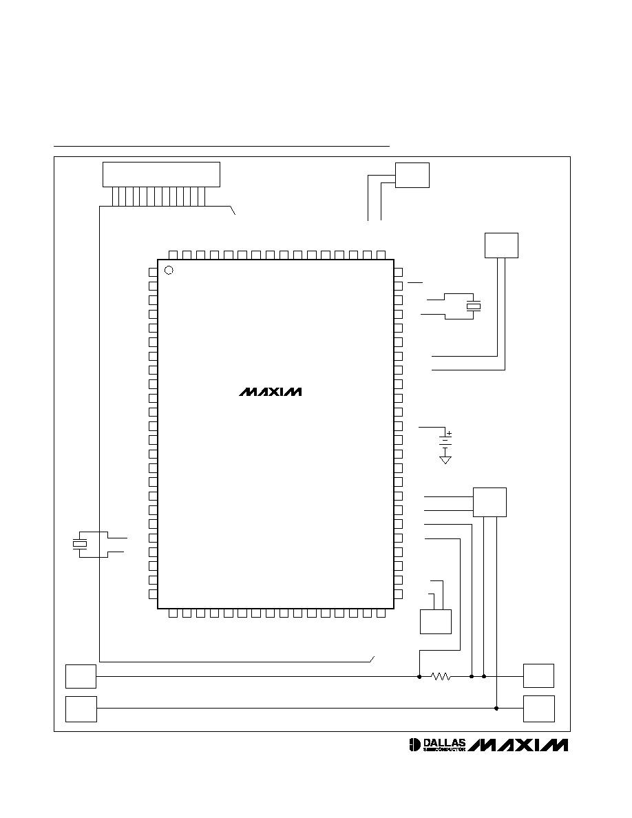
MAXQ3120
High-Precision ADC
Mixed-Signal Microcontroller
32
____________________________________________________________________
Typical Operating Circuit
80
79
78
77
76
75
74
73
72
71
70
69
68
67
66
65
25
26
27
28
29
30
31
32
33
34
35
36
37
38
39
40
P1.4/SEG15
P1.3/SEG16
P1.2/SEG17
P1.1/SEG18
P1.0/SEG19
DGND
DV
DD
N.C.
N.C.
P0.7/T2B
P0.6/T2A
64
P0.0/SQW
RESET
32KOUT
32KIN
DV
DD
DGND
P3.7/RXD1
P3.6/TXD1
P3.5
P3.4
P3.3/TCK
V
BAT
AGND
V
REF
N.C.
N.C.
AN1+
AN1-
AN0+
AN0-
AV
DD
DGND
P3.2/TMS
P3.1/TDI
P1.5/SEG14
LCD DISPLAY
P1.6/SEG13
P1.7/SEG12
SEG11
SEG10
SEG9
SEG8
SEG7
SEG6
SEG5
SEG4
V
LCD
V
LCD1
V
LCD2
V
ADJ
SEG3
SEG2
SEG1
DGND
HFXIN
HFXOUT
8MHz
DV
DD
SEG0
COM3
63
62
61
60
59
58
57
56
55
54
53
52
51
50
49
48
47
46
45
44
43
42
41
1
2
3
4
5
6
7
8
9
10
11
12
13
14
15
16
17
18
19
20
21
22
23
24
P0.5/INT2/T1
P0.4/INT1/T0
P0.3/INT0/T0G
P0.2/TXD0
P0.1/RXD0
COM2
COM1
COM0
P2.0/SEG20
P2.1/SEG21
P2.2/SEG22
P2.3/SEG23
P2.4/SEG24
P2.5/SEG25
P2.6/SEG26
N.C.
N.C.
DGND
DV
DD
P2.7/SEG27
P3.0/TDO
MAXQ3120
INFRARED
Tx/Rx
32.768kHz
RS-485
Tx/Rx
VOLTAGE-
DIVIDER
AC LINE
OUT
SERIAL
EEPROM
CURRENT
SHUNT
AC
NEUTRAL
OUT
AC LINE
IN
AC
NEUTRAL
IN

MAXQ3120
High-Precision ADC
Mixed-Signal Microcontroller
Maxim cannot assume responsibility for use of any circuitry other than circuitry entirely embodied in a Maxim product. No circuit patent licenses are
implied. Maxim reserves the right to change the circuitry and specifications without notice at any time.
Maxim Integrated Products, 120 San Gabriel Drive, Sunnyvale, CA 94086 408-737-7600 ____________________ 33
© 2005 Maxim Integrated Products
Printed USA
is a registered trademark of Maxim Integrated Products, Inc.
is a registered trademark of Dallas Semiconductor Corporation.
Quijano
Package Information
(The package drawing(s) in this data sheet may not reflect the most current specifications. For the latest package outline information,
go to www.maxim-ic.com/DallasPackInfo).
Revision History
Rev 0; 7/05:
Original release.
Rev 1; 8/05:
Added clarification to ADC Resolution condition (No missing codes, with software lowpass filter, see
Appendix A).
Deleted paragraph on Integral Nonlinearity.