 | –≠–ª–µ–∫—Ç—Ä–æ–Ω–Ω—ã–π –∫–æ–º–ø–æ–Ω–µ–Ω—Ç: PCI-30259 | –°–∫–∞—á–∞—Ç—å:  PDF PDF  ZIP ZIP |
PCI-416
Ultra-Performance, Analog Input
Boards for PCI Computers
Æ
Æ
FEATURES
∑∑
∑∑
∑
The ideal array-processor "front end"
∑∑
∑∑
∑
Up to 10MHz A/D sampling rates
∑∑
∑∑
∑
Choice of 12, 14 or 16-bit A/D resolutions
∑∑
∑∑
∑
Wideband inputs with low harmonic distortion
∑∑
∑∑
∑
Quick, 32-bit, PCI block transfers
∑∑
∑∑
∑
2 to 16-channel simultaneous sampling eliminates
phase skew
∑∑
∑∑
∑
On-board A/D FIFO memory holds 8k samples
∑∑
∑∑
∑
64 megasamples or greater data streaming
∑∑
∑∑
∑
Pre/post-trigger, gap-free, ring buffering
∑∑
∑∑
∑
Great for DSP, FFT's, digital filtering, etc.
∑∑
∑∑
∑
Pentium
Æ
compatible; Windows 95/NT software
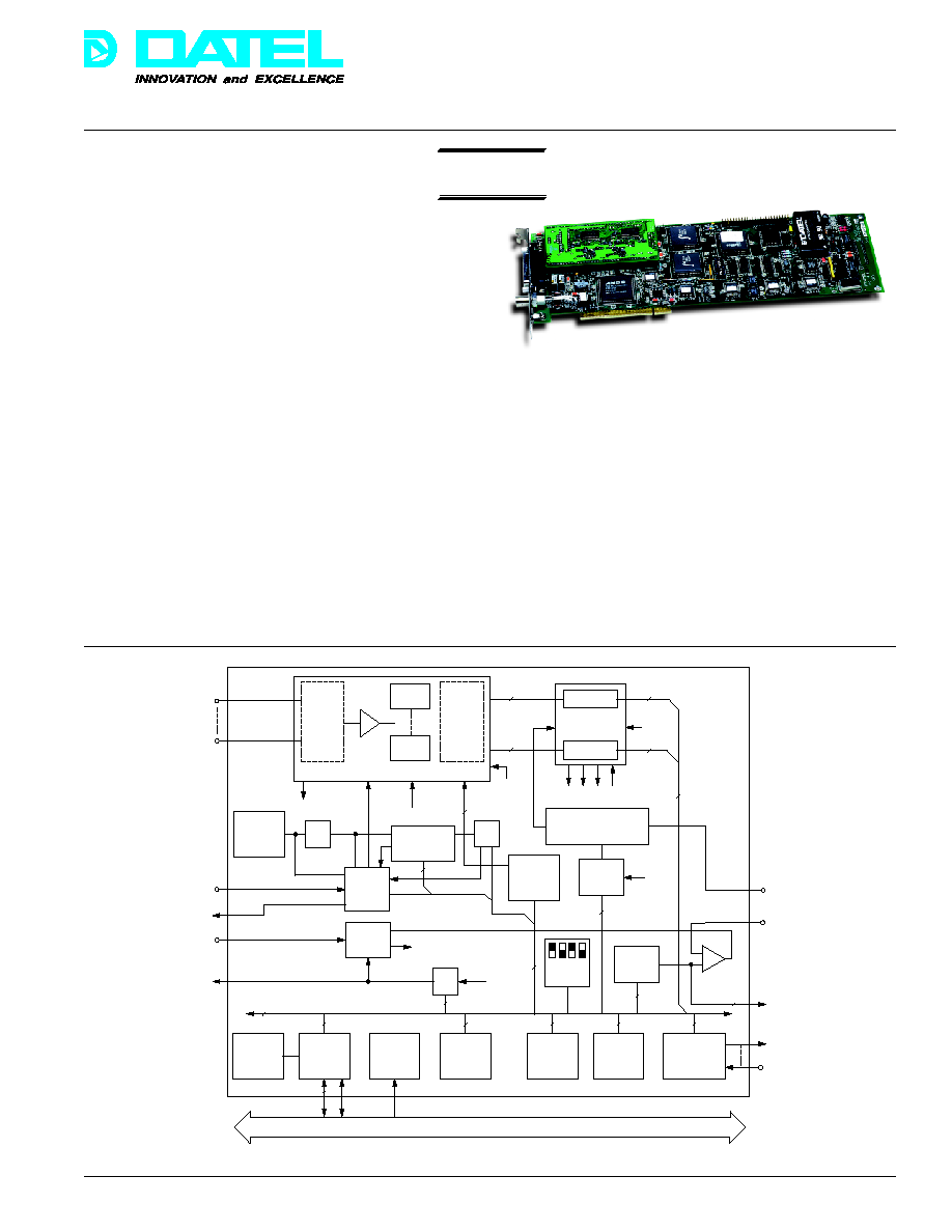
The PCI-416 Family consists of several advanced-performance,
data acquisition boards based on the 32-bit PCI bus architecture.
With an emphasis on continuous, non-stop, high-speed
streaming of A/D samples to host memory or disk, the system
has been optimized for a wide range of signal-processing and
data-recording applications. In very long "baseline" studies or
high-speed transient analysis, the PCI-416 can collect huge
amounts of "seamless" digitized data to host memory.
Exploiting a unique "banked" FIFO architecture, the PCI-416
moves two A/D words in each 32-bit PCI transfer. The FIFO
memory (8k samples deep) serves to decouple the precise
timing of the A/D converter from the block bursts of the PCI bus.
The PCI-416's optional analog front ends utilize DATEL's low-
noise, wide-bandwidth sampling A/D converters. All models
exhibit excellent harmonic distortion and perform well in DSP/
FFT applications. Software for Windows 95, NT, DOS,
Hyperception and LabVIEW
Æ
implements a menu-driven,
"no-programming", fast data recording and display system to
memory or disk.
Several different "pluggable" analog options offer up to 16 input
channels in single-ended or differential configurations, multiple
input ranges, sampling rates to 10MHz, 12/14/16-bit A/D
resolutions, and various simultaneous sampling configurations
(1 A/D per channel) up to 16 channels. The simultaneous feature
is intended for parallel sampling applications that cannot tolerate
phase skew introduced by the A/D system. These include sonar
or acoustic sensor arrays, cross-channel computation, multiple
Pluggable Analog Section
Analog
Inputs
MUX
EOC
A/D
Control
40MHz
Crystal
Oscillator
Clock
Control
˜4
10MHz
Frequency
Synthesizer
16
Bank
Switch
Sample
Counter
EOC
31-16
15-0
E
H
F RST
Pretrigger Logic, Clock
Gating, Marker
Channel
Address
Control
Trigger
ANATRG
INTTRIG
˜2
32
10MHz
82C54
32-Bit Local Bus
Module
ID
D/A
Converter
Trigger
Comparator
Analog
Trigger
Analog
Output
PCI bus
Controller
DC/DC
Power
Converter
System
Control
Status
Register
Command
Register
Parallel I/O
Port 82C55
24-Bit
Digital
I/O
Marker
Input
IRQ
Marker
SSH
Start
External
A/D
Clock
Clock
Out
External
Trigger
Trigger
Output
˜2
A/D
PCI Bus
FIFO
Memory
Bootstrap
EPROM
RST
TRIG
SEL
Pluggable Analog Section
Figure 1. Functional Block Diagram
DATEL, Inc., Mansfield, MA 02048 (USA)
∑
Tel: (508)339-3000, (800)233-2765 Fax: (508)339-6356
∑
Email: sales@datel.com
∑
Internet: www.datel.com
7
Hyperception
Win95/NT Software
NEW

Æ
Æ
PCI-416
DATEL, Inc., Mansfield, MA 02048 (USA)
∑
Tel: (508)339-3000, (800)233-2765 Fax: (508)339-6356
∑
Email: sales@datel.com
∑
Internet: www.datel.com
carrier demodulation, interferometry, multi-channel
spectrometers, and highly concurrent system testing. High-
quality, wide-bandwidth, low-noise A/D's and analog components
are used. The design is ideal as an array processor "front end"
or for DSP/FFT (Digital Signal Processing/Fast Fourier
Transform) usage.
Two on-board software-programmable timebases run the A/D
sample clock. A 40MHz frequency synthesizer provides high
resolution, whereas the 10MHz 16-stage programmable divider
offers very low clock jitter. If preferred, external clocks can be
used for both the A/D start clock and the trigger. And several
PCI-416's can be connected in master-slave clocking for many
simultaneous channels. A programmable 24-bit sample counter
collects long blocks up to 16 million samples. The trigger system
collects a single fixed length frame, N repeating frames
separated by programmable delays, or it can run "forever".
Interrupts to the PCI bus are programmable from the FIFO half
full flag, the bus master block transfer done, or the sample
counter.
System features optimize gapless sampling without data loss. A
pretrigger system can collect data continuously to host circular
memory (ring buffer) of several megabytes or more. When an
external trigger is received, the PCI-416 will count down the
number of preloaded post-trigger samples then automatically
stop when all samples are collected. The trigger sample may
then be found using a negative circular offset into the ring buffer,
knowing the post-trigger sample count.
In addition, a digital marker input will tag data samples on the fly
as often as needed. This provides later identification of external
events without stopping sample collection. A D/A analog output
is included to set the trip level to generate an external analog
triggers. Or the D/A can be used for analog output.
A general-purpose, 24-bit (82C55) digital I/O port which is
separate from the fast A/D parallel port can control external
circuits. The parallel port uses an internal header connector.
Like any PC hardware, the PCI-416 needs software to command
and control it. Data acquisition, data display and data storage
applications are available for Windows
Æ
95/98, Windows
Æ
NT,
Hyperception, National Instrument's LabVIEW
Æ
, and MS-DOS
Æ
.
Simply install the software on your PC and you will be acquiring
and storing data within minutes. When data acquisition is
complete, any third party data processing application can be
used to analyze the results. Non-programmers will be very
interested in our Hyperception and LabVIEW
Æ
driver libraries.
These visual programming environments allows you to create
custom Windows
Æ
95/98 virtual instruments for test and
measurement applications, without writing code.
Programmers developing their own code may need to customize
the system to better suit an application, or simply to integrate the
PCI-416 with existing software. Professionally written, well
commented source code for all of DATEL's software is available.
Everything from dynamic link library (DLL) functions to graphic
user interface (GUI) modules are provided to accommodate all
levels of software development. The software was designed
using common integrated development environments such as
C/C
++
, Delphi
Æ
, and C
++
Builder
Æ
. To help with your development
efforts, most source code is accompanied with comprehensive,
well written reference manuals. If you run into problems along
the way, you can rely on DATEL's team of highly qualified
technical support and applications engineers to guide you
through.
REGISTER I/O or MEMORY MAPPING
All of the PCI-416's registers require 32-bit instructions.
DATEL software provides highly portable examples which can
be used with any language. All registers are fully described in
the User Manual included with the board.
Base Address
Register
Function
BADR0
S5933 PCI controller operation registers
BADR1
Pass-Thru Address Register Latch (ARL)
BADR2
Read/Write general registers
If ARL=0,
Command register (write only)
If ARL=4,
Sample counter (write only)
If ARL=8,
Channel address register (write)
Clear A/D FIFO memory (read)
If ARL=12, A/D convert enable (write only)
If ARL=16, PLL register (write only)
BADR3
High-speed read of status register or A/D
FIFO data
If ARL=0,
Status register (read only)
If ARL=4,
A/D FIFO data (read only)
BADR4
Low-speed devices, 82C54 and 82C55, and
analog output
82C54 Programmable counter-timer (read/write)
If ARL=0,
Counter 0
If ARL=4,
Counter 1
If ARL=8,
Counter 2
If ARL=12, Control register
82C55 Programmable parallel port (read/write)
If ARL=16, Port A
If ARL=20, Port B
If ARL=24, Port C
If ARL=28, Control register
Analog output (D/A channel)
If ARL=32, D/A converter register (write
only)
8

Æ
Æ
PCI-416
DATEL, Inc., Mansfield, MA 02048 (USA)
∑
Tel: (508)339-3000, (800)233-2765 Fax: (508)339-6356
∑
Email: sales@datel.com
∑
Internet: www.datel.com
FUNCTIONAL SPECIFICATIONS
(Typical at +25∞C, dynamic conditions, gain = 1, unless noted)
PCI-416F
2 Simultaneous
Single Ended
0 to +10 V
±5 V
±15 V
2 µs
--
>1 M
165 ns
20 ns
±40 ps
12 bits
400 ns
2
±1
±1
±0.1
±0.1
2 MHz
2 MHz/chan.
≠70 dB
PCI-416E
16SE/8D
SE or Diff.
0 to +10 V
±10 V
±5 V
[Footnote 1]
±15 V
2 µs
±10 V
100 M
750 ns
20 ns
±40 ps
12 bits
500 ns
1
±1
±0.75
±0.1
±0.1
2 MHz
31.25 kHz/chan.
≠72 dB
PCI-416B
4
Single Ended
0 to +10 V
±10 V
±5 V
±15 V
2 µs
--
10 M
750 ns
20 ns
±100 ps
14 bits
1.6 µs
1
±1.5
±1
±0.3
±0.3
500 kHz
82 kHz/chan.
≠75 dB
ANALOG INPUTS
Number of Channels
Input Configuration
(non-isolated) [Footnote 15]
Full Scale Input Ranges
(user-selectable)
(gain = 1)
Input Overvoltage
(no damage, power on)
Overvoltage Recovery
Time, maximum
Common Mode Voltage
Range, maximum
Input Impedance
Acquisition Time
Aperture Delay
Aperture Delay Uncertainty
Resolution
Conversion Period
Number of A/D Converters
Integral Non-linearity
(LSB of FSR)
Differential Non-linearity
(LSB of FSR)
Full Scale Temperature
Coefficient (LSB per ∞C)
Zero or Offset
Temperature Coefficient
(LSB per ∞C)
Sample Rate
(single channel only)
Sample Rate per Channel
(simul. or sequential chans.)
[Footnote 4]
Total Harmonic Distortion
[Footnote 3]
PCI-416D
1
Differential
±5 V
(0 to +10 V,
special order)
±15 V
2 µs
±1 V
2 k
50 ns
10 ns
±7 ps
12 bits
200 ns
1
±2
±1
±0.1
±0.3
5 MHz
--
≠68 dB
SAMPLE/HOLD
A/D CONVERTER
SYSTEM DC CHARACTERISTICS [Footnote 6]
SYSTEM DYNAMIC PERFORMANCE [Footnote 2]
Note:
Model PCI-416J in short-cycled addressing is recommended in place of the PCI-416A.
Model PCI-416E can substitute for the PCI-416C.
ANALOG INPUTS
Programmable Gains
See Footnote 1
Common Mode Rejection
(DC - 60 Hz)
-80 dB (g = 100) (416E)
Addressing Modes
1. Single channel
(short cycle channel
2. Simultaneous sampling
addressing is software-
3. Sequential with
selectable on PCI-416J,L)
autosequenced addressing
4. Random addressing by host
software
A/D CONVERTER
Output Coding
Positive-true, right justified,
straight bin. (unipolar) or right-
justified 2's comp. (bipolar) with
sign extension thru bit 15
Warm-Up Period
20 minutes until rated
specifications. [Footnote 6]
Please read all footnotes carefully.
9

Æ
Æ
PCI-416
DATEL, Inc., Mansfield, MA 02048 (USA)
∑
Tel: (508)339-3000, (800)233-2765 Fax: (508)339-6356
∑
Email: sales@datel.com
∑
Internet: www.datel.com
ANALOG INPUTS
Number of Channels
Input Configuration
(non-isolated) [Footnote 15]
Full Scale Input Ranges
(user-selectable)
(gain = 1)
Input Overvoltage
(no damage, power on)
Overvoltage Recovery
Time, maximum
Common Mode Voltage
Range, maximum
Input Impedance
Acquisition Time
Aperture Delay
Aperture Delay Uncertainty
Resolution
Conversion Period
Number of A/D Converters
Integral Non-linearity
(LSB of FSR)
Differential Non-linearity
(LSB of FSR)
Full Scale Temperature
Coefficient (LSB per ∞C)
Zero or Offset
Temperature Coefficient
(LSB per ∞C)
Sample Rate
(single channel only)
Sample Rate per Channel
(simul. or sequential chans.)
[Footnote 4]
Total Harmonic Distortion
[Footnote 3]
FUNCTIONAL SPECIFICATIONS
(Typical at +25∞C, dynamic conditions, gain = 1, unless noted)
PCI-416K
2 Simultaneous
Limited Differential
0 to +10 V, ±5 V
(separate
models)
±15 V
--
±1 V
1 k
50 ns
10 ns
±7 ps
12 bits
200 ns
2
±2
±1
±0.1
±0.3
5 MHz
5 MHz/ch.
≠68 dB
PCI-416G
2 Simultaneous
Single Ended
±5 V or
0 to +10 V
(separate
models)
±15 V
2 µs
--
>1 M
350 ns
20 ns
±70 ps
14 bits
1 µsec*
2
±1.5
±1
±0.3
±0.3
1 MHz*
1 MHz/chan.*
≠80 dB
PCI-416H
1
Differential
±5 V
(other ranges
special order)
±15 V
1 µs
±1 V
2 k
35 ns
±10 ns
3 ps rms
12 bits
100 ns
1
±1.5
±1
±1
±1
10 MHz
--
≠65 dB
PCI-416J
8 Simultaneous
Single Ended
±5 V, ±10 V
[Footnote 10]
±15 V
--
--
8 k
(bipolar)
400 ns
--
--
12 bits
2 µs
(all chans. in
simul. sampling)
8
±1
±1
[Footnote 10]
[Footnote 10]
400 kHz
250 kHz/chan.**
≠75 dB
SAMPLE/HOLD
A/D CONVERTER
SYSTEM DC CHARACTERISTICS [Footnote 6]
SYSTEM DYNAMIC PERFORMANCE [Footnote 2]
*Dual 2MHz 14-bit sampling is available on special order, model PCI-30267.
**A 380kHz/channel option is available on special order, model PCI-30264.
10
Æ
Æ
PCI-416
DATEL, Inc., Mansfield, MA 02048 (USA)
∑
Tel: (508)339-3000, (800)233-2765 Fax: (508)339-6356
∑
Email: sales@datel.com
∑
Internet: www.datel.com
FUNCTIONAL SPECIFICATIONS
(Typical at +25∞C, dynamic conditions, gain = 1, unless noted)
ANALOG INPUTS
Number of Channels
Input Configuration
(non-isolated) [Footnote 15]
Full Scale Input Ranges
(user-selectable)
(gain = 1)
Input Overvoltage
(no damage, power on)
Overvoltage Recovery
Time, maximum
Common Mode Voltage
Range, maximum
Input Impedance
Acquisition Time
Aperture Delay
Aperture Delay Uncertainty
Resolution
Conversion Period
Number of A/D Converters
Integral Non-linearity
(LSB of FSR)
Differential Non-linearity
(LSB of FSR)
Full Scale Temperature
Coefficient (LSB per ∞C)
Zero or Offset
Temperature Coefficient
(LSB per ∞C)
Sample Rate
(single channel only)
Sample Rate per Channel
(simul. or sequential chans.)
[Footnote 4]
Total Harmonic Distortion
[Footnote 3]
PCI-416L
16 Simultaneous
Single Ended
±5 V, ±10 V,
(user selectable)
[Footnote 10]
±15 V
--
--
8 k
400 ns
--
--
12 bits
2 µs
(all chans. in
simul. sampling)
16
±2
±1
[Footnote 10]
[Footnote 10]
400 kHz
190 kHz/chan.
-75 dB
PCI-416M
4 Simultaneous
Single Ended
±10 V
±12 V
--
--
10 M
2 µs
--
--
16 bits
5 µs
(all chans. in
simul. sampling)
4
±4
±3
±1
±1
200 kHz
200 kHz/chan.
-83 dB
PCI-416N
2 Simultaneous
Single Ended
±2.5 V
±15 V
--
--
10 M
or 50
35 ns
±10 ns
5 ps
14 bits
200 ns
(all chans. in
simul. sampling)
2
±1
±1
±0.5
±0.5
5 MHz
5 MHz/chan.
-75 dB
PCI-416P
4 Simultaneous
A/D's
Single Ended
±2.5 V or
0 to +5 V
(user selectable)
±7 V
--
--
1000
80 ns
--
--
14 bits
400 ns
4
±3
±1.5
±0.5
±0.5
3 MHz* min.
2.5 MHz/chan.
-75 dB
SAMPLE/HOLD
A/D CONVERTER
SYSTEM DYNAMIC PERFORMANCE [Footnote 2]
SYSTEM DC CHARACTERISTICS [Footnote 6]
* The sample rate to published specifications is 3 MHz. The A/D is functional to 5 MHz. Valid data output per channel is delayed
by 4 samples after the start of the sample clock. Please make note of this for products such as the PC-414P, PC-430P, and
DVME-614P which use non-continuous A/D sampling. Data output is pipelined meaning that the first four samples per channel
should be discarded. For all 4 channels, discard 16 samples. The design is intended for semi-continuous sampling of wideband
signals and is less suitable for low speed data acquisition. Approximately 5 dB SFDR improvement can be achieved by directly
connecting an external A/D sample clock. Contact DATEL for details.
11

Æ
Æ
PCI-416
DATEL, Inc., Mansfield, MA 02048 (USA)
∑
Tel: (508)339-3000, (800)233-2765 Fax: (508)339-6356
∑
Email: sales@datel.com
∑
Internet: www.datel.com
SPECIFICATIONS, CONTINUED
(Typical @ +25∞C, dynamic conditions, unless noted)
A/D SAMPLE CLOCK
Sample Clock Sources
Selectable from among:
[Footnote 7]
1. Frequency synthesizer*
2. 10MHz crystal oscillator
3. 20MHz crystal oscillator
4. 16-stage binary divider
to either 1 or 2, maximum
input: 10MHz
5. External digital input
Frequency Synthesizer
Output 5-10MHz in 625Hz
(not available on PCI-416N2)
steps, further divisible by 16-
stage binary divider, all
software programmable. Up
to 40MHz is available in
2500Hz steps.
Total Sample Range
76.3Hz to 10MHz
(40MHz available)
Oscillator Frequency
Accuracy
±50ppm (+20 to +30∞C)
Crystal Aging
±5ppm/year
Trigger Sources
1. Analog threshold
[Footnote 8]
comparator using internal
D/A to set trip level**
2. Internal trigger derived
from10MHz timebase,
divided by 32-stage
divider (82C54). Range:
20ns to 429.5 seconds.
3. External digital trigger
Trigger Response
Selectable from among:
1. Starts one frame ("single
trigger mode")
2. Collects repeating
frames, each started by
a trigger ("continuous
trigger mode").
3. Runs the A/D "forever"
(sample counter disabled)
A/D Samples per Frame
1 to 16,777,216 samples
(24-bit counter) or "forever"
Analog Trigger Input Range
±10V
Analog Trigger Response
2µs [Footnote 5]
Analog Trigger Hysteresis
±40mV
Marker Input
Digital input which sets A/D
bit 15 to logic "1" for one A/D
clock cycle. Used to tag
samples to external events if
enabled.
Pretrigger Mode
The sample down-counter is
delayed until an external
trigger. Pretrigger samples
are stored in a host ring
buffer for transient capture, if
enabled.
ANALOG OUTPUT (not available on PCI-416N2)
Number of Channels
One channel
Function
Selectable from among:
1. General-purpose analog
output
2. Threshold comparator for
A/D trigger
Resolution
12 bits
Output Voltage Range
0 to +10V, ±5V, ±10V at 5mA
max. (user selectable)
Linearity
±0.05% of FSR
Settling Time
5 microseconds (10V step)
Input Coding
Straight binary
Data Bus Size
32 bits
Address Bus Size
32 bits
PCI Controller Type
AMCC S5933 bus master or
slave mode
Data Transfer
32-bit I/O or memory
(selectable)
Bus Transfer Mode
Up to 2
24
longwords, per
PCI spec.
Interrupt
One interrupt, selectable to
INTA, B, C, or D
Interrupt Sources
FIFO half full, sample count
reached (ACQuire flag), bus
master transfer done.
Board Identification Switch
4-bit DIP switch is factory
preset to identify A/D module
type. May be changed if
another module is used.
Analog Section Modularity
The MUX-S/H-A/D module is
socketed for function
interchange.
Analog Section
Offset and gain per channel
Adjustments
for SSH on PCI-416F,G,K,M,N.
A single offset and gain pot is
provided on PCI-416B,D,E.
Recommended recalibration
interval is 90 days in stable
conditions.
Operating Temp. Range
0 to +60∞C, thermal shock
±1∞C max per minute.
Storage Temp. Range
-25 to +85∞C
Humidity
10% to 90%,
non-condensing
Altitude
0 to 10,000 feet, forced
cooling is required
Power Required
+5Vdc @ 3.0A max. from
PCI bus. Compatible to
+3.3V systems but makes no
connection.
Outline Dimensions
4.2 x 12.28 x 0.5 inches,
compatible to PCI bus
Architecture
First-In, First-Out (FIFO)
Memory Capacity
8192 A/D samples
TRIGGER CONTROL
PCI Bus
MISCELLANEOUS
A/D MEMORY
*No frequency synthesizer on PCI-416N2.
**No analog trigger on PCI-416N2.
12

Æ
Æ
PCI-416
DATEL, Inc., Mansfield, MA 02048 (USA)
∑
Tel: (508)339-3000, (800)233-2765 Fax: (508)339-6356
∑
Email: sales@datel.com
∑
Internet: www.datel.com
6.
Allow 20 minutes warmup time to rated specifications for
models PCI-416B,G,M,N.
7.
Use the crystal oscillator for best harmonic performance.
8.
Avoid mixing external triggers which are a close
submultiple of the internal A/D start clock to prevent
sample jitter.
9.
The BNC connector may be rewired to either external
trigger or external A/D clock.
10. PCI-416J and 416L bipolar input is user-selectable ±5V
or ±10V (default) per channel. Total gain error over
temperature range is ±4 LSB maximum. Total zero/offset
error over temperature range is ±4 LSB maximum.
Monotonicity: no missing codes over temperature range.
11. Input polarity. Some models are fixed as bipolar only
whereas others are user-selectable unipolar or bipolar.
Still others require separate model numbers.
12. PCI-416D, H, and K, inputs are jumpered as single-
ended. Special, user-configured wiring allows differential
operation.
13. Models F, G, J, K, L, M, N, and P use one A/D converter
per channel.
14. The customer must use shielded cables to insure EMC
compliance.
15. A/D-per-channel boards (models F, G, J, K, L, M, N, P)
may be operated in "software differential" mode. Two A/D's
are applied to the high and low legs of a single
differential input channel. The two data values are then
algebraically subtracted, either on the fly in real time or
after all samples have been stored. Channel capacity in
"software differential" is one-half the number of single-
ended channels.
This technique offers excellent bandwidth, high common
mode rejection and optional mix of single-ended and
differential channels.
FOOTNOTES
1.
Resistor-programmed gain (user supplied) from x1 to
x100 is available on PCI-416E with increased settling
delay at higher gains. Requires precision gain resistor.
2.
Total throughput includes MUX settling time after
changing the channel address, S/H acquisition time to
rated specifications, A/D conversion, and FIFO transfer.
Total throughput is not delayed by host software
whenever the FIFO is not full.
3.
THD test conditions are:
1. Input freq.
500kHz (416F)
200kHz (416B,E,G)
50kHz (416J,L,M)
1MHz (416D,K)
2MHz (416H)
2. Generator/filter THD is -90dB minimum.
3. THD computed by FFT to 5th harmonic.
( V2
2
+ V3
2
+ V4
2
+ V5
2
)
0.5
Vin
4. Inputs are full scale less 0.5dB. No channel advance.
5. A/D sample rate = 500kHz (416B,E,G), 5MHz (416D,K),
2MHz (416F), 10MHz (416H), 250kHz (416J),
190kHz (416L,M)
6. Crystal oscillator is used.
4.
The rates shown for sequential sampling are the
maximum A/D converter start rates and include MUX
sequencing and settling. For example, if four channels
of the PCI-416E were scanned, the maximum sample
rate on any one channel would be 2µs x 4 channels =
8µs (125kHz per channel).
5.
For fastest response on the analog comparator trigger,
keep the reference voltage near the trip input voltage. To
avoid overload recovery delays, do not let the trip input
(or any other analog input) exceed ±10V.
log10
( )
THD = 20
Marker Input
When selected in the Command Register, the marker input is
for tagging A/D samples to an external event such as a clock
timebase. The marker sets bit 15 of the A/D word to logic "1"
for one sample clock cycle. Lower A/D bits still retain sign
extension polarity. This tag is now stored in the FIFO along
with the A/D sample. The user may do this as often as
needed, and the marker can be asynchronous with the A/D
sample clock. Post processing software then searches
through the saved data to find each marked sample. The
marker bit is not available for 16-bit A/D's.
15
14 - 11
10 - 0
M
Sign/MSB
A/D Data
Marker input sets bit 15 = 1. Otherwise, bit 15 = 0.
(12-bit A/D shown)
Figure 2. Marker Sample Tagging
CONNECTORS
PCI bus
120-pin (dual 60) PCI
edgeboard connector
Analog Input
DB-25 25-pin connector
(Model PCI-416P2
mounted on rear plate.
always includes SMA
Miniature threaded coaxial
connectors)
SMA connectors are
available under special order
for 4 input channels or less.
External Trigger
[Footnote 9]
On DB-25 analog connector
External A/D Clock In
BNC coaxial on rear plate
Digital I/O Port
Internal header connector.
External clock, D/A mounted
on board interior, suitable for
flat cables.
Configuration
24 lines, programmable as
input or output with latches
and handshakes
Controller
82C55
Levels
TTL logic, 1 TTL load in or
out (direct from 82C55)
Outport Settling Time
50ns, after write operation
DIGITAL I/O PORT
13

Æ
Æ
PCI-416
DATEL, Inc., Mansfield, MA 02048 (USA)
∑
Tel: (508)339-3000, (800)233-2765 Fax: (508)339-6356
∑
Email: sales@datel.com
∑
Internet: www.datel.com
A/D Data Format
A/D data is delivered as a stream from the FIFO memory.
For multichannel inputs, this means that data is multiplexed by
the channel address with a modulo address wrap-around at
the top channel. For example, with 4-channel inputs, the
output channel sequence is 0, 1, 2, 3, 0, 1, . . . One additional
factor is that the 32-bit wide dual FIFO contains two A/D
samples. Therefore the longword sequence is 0,1 . . . 2,3 . . .
0,1 . . .
The FIFO output can take two formats depending on which
analog module is used and whether single-channel or
autosequential (autoincrement) channel addressing is
selected. For single-channel mode, data appears as follows:
31 16
15 0
Sample N+1
Sample N
If the addressing is selected for autoincrement, data appears
this way:
31 16
15 0
Channel N+1 Channel N
Note that all A/D data is right-justified within the 16-bit data
word with sign extension to bit 15 or 31. Also be aware that
the PCI-416 uses "Intel" or little-endian addressing where
lower (or earlier) data is lower in word memory.
Setup and A/D Collection Software
Software is available for Windows
Æ
95/98, NT, MS-DOS,
Hyperception and LabVIEW
Æ
. Source code is available for
developers.
∑
Performs PCI BIOS verification and setup
∑
Automatically configures to the display adapter, CPU and
memory
∑
Initializes the interrupt and bus master systems and D/A
output
∑
Allocates base or extended memory
∑
Performs self-test and A/D-D/A calibration
∑
Configures A/D sample rate, frame rate and sample
counter
∑
Selects trigger mode and bus master or I/O block transfer
∑
Selects disk file output format to integer binary
∑
Saves data to base memory, extended memory or disk
∑
Full source code in "C" and assembly is available
PCI-416 Hyperception Block Diagram Signal Processing
System
Models PCI-416HYP and PCI-416HYPL.
∑
Advanced Windows 95/NT A/D conversion and data
collection software library. Please refer to the
PCI-416HYP/L data sheet.
∑
Object-oriented visual environment using graphical
programming "Block Language" connecting icons.
∑
Ideal for fast simulations, modeling, prototyping.
∑
Powerful nested hierarchical capabilities - build your own
icon library.
∑
Comprehensive screen graphics, printer support.
∑
Hundreds of DSP, FFT, filter, control, A/D and math
functions.
∑
Optional "C" source code generation or integrate your own
code.
∑
Two versions: PCI-416HYPL ("Block Lite") includes almost
100 common functions. PCI-416HYP offers full library
with several hundred operations.
PCI-416HYP Screen Capture
14

Æ
Æ
PCI-416
DATEL, Inc., Mansfield, MA 02048 (USA)
∑
Tel: (508)339-3000, (800)233-2765 Fax: (508)339-6356
∑
Email: sales@datel.com
∑
Internet: www.datel.com
Pre/Post Trigger Transient Capture Applications
A certain class of applications requires data sampled relative to one or more external events. Data before and after the event
need to be analyzed. If the exact time of those external events cannot be predicted accurately but the event can be identified
with a trigger, data must be recorded continuously then processed after the event occurred. At higher sample rates, the user
must use all memory storage, which has limited capacity, but is still large enough to capture the event. A ring buffer circular
storage method is used in which new samples continually overwrite the oldest samples.
Figure 4. Transient Signal Capture
The PCI-416 accepts either a digital or analog (threshold trip) event trigger. An on-board D/A converter sets the comparator
voltage level for the analog trigger. The system stores data before and after the trigger. A post trigger sample counter selects
the number of offset samples after the trigger. The number of pretrigger samples equals the total circular storage minus the post
trigger size. Note that pretrigger samples in Figure 5 are skewed over the buffer tail.
Figure 5. A/D Data Ring Buffering
A/D collection continues after the trigger until the system has stored the number of samples specified in the sample counter. The
trigger sample can be found using backwards circular offset from the last sample saved. Multiple external events can be
identified using a combination of the post trigger method and the marker inputs.
Special software available for the PCI-416 can access huge PCI memory. This requires the 80486 or Pentium CPU to enter
protected mode and transfer the data. Collected A/D samples can then be saved to disk or tape.
Analog Input
Signal
Sliding Window
Trigger
Total Circular Buffer Length
Time
Post Trigger
Pretrigger
Head
Tail
Pretrig Samples
Posttrig Samples
Pretrig Samples
Trigger
Oldest Sample
Last Sample Collected
"Offset"
Sample Count
PCI-416
Board
A/D Clock
Analog
Inputs
Streaming
Memory
Ring
Memory
Signal Processing
Software or
Spread Sheet
Graphics
Display
Disk
DSP/FFT
Board
D/A or
Control
LAN or
Data Link
User-written
Program
A/D FIFO
Block
Transfer
Pretrigger Mode
PCI-416WIN/NT/SET/LV
∑ Configure hardware
∑ Start acquisition
∑ Store data to disk
∑ View data
∑ Digital I/O port
∑ A/D-D/A calibration
Optional
Interleaved
Operation
Start and
Exit Mode
Output Resources
Figure 3. PCI-416 Software Data Flow
15

Æ
Æ
PCI-416
DATEL, Inc., Mansfield, MA 02048 (USA)
∑
Tel: (508)339-3000, (800)233-2765 Fax: (508)339-6356
∑
Email: sales@datel.com
∑
Internet: www.datel.com
Highly Parallel Array Sampling
Although the F, G, J,K, L, and N models of the PCI-416 offer
unique high-performance simultaneous-sampling capabilities,
this can be extended by connecting several PCI-416's in
parallel. A master PCI-416 can distribute its internal trigger
signal to several other 416's for concurrent sampling with
practically no phase lag. Applications include sensor arrays,
astrophysics, biomedical sampling, engine cells, multichannel
audio, and aerospace structure testing.
Two interconnection methods accommodate either externally
or internally triggered applications. External triggers simply
connect in parallel to all PCI-416's. Each board is armed with
its sample count and clocking systems to perform parallel
sampling. Only one board sends interrupts. When data is
ready, the host computer rapidly retrieves data blocks from
each board in sequence.
For internal triggers, one board is the master generating
triggers for itself and for all other boards. Slave 416's attach
to the master 416's trigger output connection.
Trigger and Sample Count Systems
The PCI-416 accepts one of three triggers - external analog,
internal or external digital. All three initiate identical internal
actions. For the internally generated trigger, either a single
trigger can be accepted ("single trigger mode") or the trigger
can repeat ("continuous trigger mode") with programmable
delays between each trigger.
Internal trigger rates are independent from but synchronous to
the internal programmable A/D clock rate. The trigger starts a
frame of samples. Each frame can be from one to 16,777,216
samples using the 24-bit counter. The system will collect the
number of samples in the sample counter then stop and wait
for the next trigger. Meanwhile, the sample counter will
automatically reload in anticipation of the next trigger. This
sample counter may be disabled by software for non-stop
continuous streaming past 16 megasamples after the trigger.
Data flows into the FIFO memory which will notify the host
that it has data to be saved. The FIFO size is independent of
the frame size, therefore FIFO flags will occur separately from
the sample counter.
A PCI bus interrupt can be generated after each frame
completes (the "ACQuire" interrupt), or at each FIFO half full
signal. Interrupt is also available after each bus master block
transfer.
Three basic trigger modes are offered. A single trigger will
start one frame then stop. The continuous trigger mode will
generate repeating frames. In the last "forever" mode, the
sample counter is disabled. A single trigger will start sampling
indefinitely. The host computer must then externally decide
when to stop sampling.
The PCI-416 will automatically control its own channel
addressing such that the address advances immediately as a
sample is sent to the FIFO. In single-channel mode, each
frame will consist of data from only the selected channel. In
automatic sequential addressing ("autoincrement"), the frame
will contain one or more scans of channels, with addresses
automatically wrapping around according to the channel
capacity of the analog module.
The combination of programmable sample count, frame rate,
A/D rate, and channel addressing mean that practically all
conceivable applications can be done. The basic system
timing is shown in Figure 8.
Trigger
416F
416F
416F
Chan. 0,1
Chan. 2,3
Chan. x, x + 1
For an external trigger . . .
Trig Out
416F
416F
416F
Master
Slave 0
Slave N
Trig In
For an internal trigger . . .
Figure 6. Highly Parallel Simultaneous Sampling
System Throughput
All specifications listed here describe performance available
on the
board. Actual transfer rates out to system memory,
disk, network, or other data destinations depend on many
other factors. These include the memory type and memory
controller, host software Operating System, disk interface,
number of disk drives, buffer sizes, type of disk controller,
number and method of simultaneous applications, DMA
usage, CPU type and speed, bus loading, software design,
etc. It is not practical to state a single set of performance
specifications for the total
system however, DATEL can give
you guidelines for a specific configuration. For speed-critical
applications, the full system must be thoroughly tested to
develop actual performance.
16

Æ
Æ
PCI-416
DATEL, Inc., Mansfield, MA 02048 (USA)
∑
Tel: (508)339-3000, (800)233-2765 Fax: (508)339-6356
∑
Email: sales@datel.com
∑
Internet: www.datel.com
Start and Exit Mode
For applications which need the data streaming continuously
to external software, the extensive library functions can easily
be interleaved with user-written code. A special "start and
exit" mode in PCI-416SET simply configures the board via
menus, starts A/D conversion then exits to the operating
system without saving any data. Next, the user's following
program (usually in a batch file) retrieves data directly from
the on-board registers or via 32-bit bus master mode. This is
simple to program and very high speed. This data collection
program may loop back repeatedly to get fast blocks of data
and the PCI-416 continues filling the FIFO while the user
program runs. This is true concurrent coprocessing with no
lost data.
Start and exit mode offers a high degree of control over the
board while avoiding time-comsuming menu design and
coding. The system will even wait for an external trigger,
giving time to set up the data collection program. Start and
exit mode can be saved to automatically run, like all other
PCI-416SET applications. A typical program flow for start and
exit is shown:
1. SETUP PCI-416 board.
2. Save configuration to disk.
3. Start A/D and exit to MS-DOS (the A/D stays running).
<start of user's program>
LOOP:
4. If the FIFO overflowed, process the error.
5. Move block of A/D data from FIFO to host memory.
6. Do other processing on A/D data block (math, disk, display,
etc.).
7. If more data is needed, GO TO LOOP.
8. Else, stop the A/D and quit.
The "Do other processing ..." step is a program written by the
user. Notice that the PCI-416 continues with non-stop A/D
sampling during this step.
Besides being a fast data recorder, PCI-416SET also
performs register tests to verify proper board operation. In
addition, PCI-416SET does calibration using an external dc
voltage source, loads data into the D/A channel and exercises
the digital I/O port.
The source code may be modified by the user (or by DATEL
under special order) to adapt to any conceivable function.
Internal or external trigger rate
TRIGGER*
A/D
START
CONVERT
END OF
SCAN*
(Internal
signal)
ACQUIRE
FLAG
Maskable Interrupt and Status
0
1
2
3
Internal or external start rate
Fixed or sequential channel addressing up to
16M samples per trigger
SSH
(Internal only)
HOLD
SAMPLE
Figure 8. PCI-416 Timing Diagram
Figure 7. PC-490A and PC-490B D-Connector
to Screw Terminal Adapters
17
Æ
Æ
PCI-416
DATEL, Inc., Mansfield, MA 02048 (USA)
∑
Tel: (508)339-3000, (800)233-2765 Fax: (508)339-6356
∑
Email: sales@datel.com
∑
Internet: www.datel.com
Input Channels, A/D Resolution
B = 4SE chans., 14 bits
J = 8SE simul. chans., 12 bits
D = 1D chan., 12 bits
K = 2SE simul. chans., 12 bits
E = 16SE/8D chans., 12 bits
L = 16SE simul. chans., 12 bits
F = 2SE simul. chans., 12 bits
M = 4SE simul. chans., 16 bits
G = 2SE simul. chans., 14 bits
N = 2SE simul. chans., 14 bits
H = 1D chan., 12 bits
P = 4SE simul. chans., 14 bits
FIFO Memory Size
2 = 8k A/D samples
Analog Input Polarity
A = Bipolar or selectable
B = Unipolar
For all models with user-
selectable input polarity,
use the "A" designator.
Caution: Read the input
range specifications
carefully.
PCI-416
ORDERING INFORMATION
2
61-7342340
SMA male to BNC male coaxial cable, 1 meter length. One cable required per channel.
PC-490B
DB-25 screw termination adapter (cable not included). Not recommended for high-frequency signals.
PCI-30259
PCI-416 less A/D module. Accepts 16-bit high-speed digital input and strobe at the module sockets.
PCI-30264
PCI-416J2 with 380kHz sampling per channel.
PCI-30267
PCI-416G2A with 2MHz sampling per channel.
UM-PCI-416
Spare user manual. One is included with board.
Software:
PCI-416SRC
Setup/configuration data-collection program for MS-DOS. Includes "C" and assembly source
PCI-416SET
code and executables. Model PCI-416SET are executable.
PCI-416WIN, WINS
Setup and data collection program for Windows 95. The source (PCI-416WINS) uses Borland C++
Builder and Visual C for the DLL and device driver.
PCI-416NT, NTS
Windows NT version of PCI-416SET/SRC. The full source code (PCI-416NTS) includes the executables
(PCI-416NT). Consists of a user interface, DLL, and device driver.
PCI-416LV, LVS
Bridge driver software to National Instruments' LabVIEW
Æ
(executables only). LabVIEW must be
purchased separately from National Instruments. Model PCI-416LVS is the source code to PCI-416LV.
PCI-416HYP, HYPL
Hypersignal Block Diagram advanced signal processing system for Windows
Æ
95/NT. See data sheet.
Free Visual BASIC example software is available on request.
Note: Software is
not included with the board. It should be added to your board order. Full software support is available only
with board purchase. All sources also include the binary executables.
Models with miniature threaded coaxial SMA connectors*.
Model Number
Number of Channels
A/D Resolution
Equivalent Root Model
PCI-30379
4SE
12 bits
PCI-416C2
PCI-30357
2SE simultaneous
12 bits
PCI-416F2
PCI-30352
2SE simultaneous
14 bits
PCI-416G2B
PCI-30343
1D
12 bits
PCI-416H2
PCI-30374
2SE simultaneous
12 bits
PCI-416K2B
PCI-30439
2SE simultaneous
12 bits
PCI-416K2A
PCI-30444
2SE simultaneous
14 bits
PCI-416N2
PCI-30447
4SE simultaneous
16 bits
PCI-416M2
PCI-416P2
4SE simultaneous
14 bits
see note
(The PCI-416P2
always includes SMA connectors.)
*Functional specifications are identical to the root model.
Example: PCI-416G2A 2SE simul. input channels, 2 14-bit 1MHz A/D's, 8k FIFO, ±5V input
Each board is power-cycle burned-in, tested and calibrated. All models include a user's manual.
Pentium is an Intel trademark
Windows and MS-DOS are Microsoft trademarks
LabVIEW is a National Instruments trademark
Hardware:
18