D
S21901 Rev. E-3 1 of 2 BS208
BS208
P≠CHANNEL ENHANCEMENT MODE DMOS TRANSISTOR
Features
∑
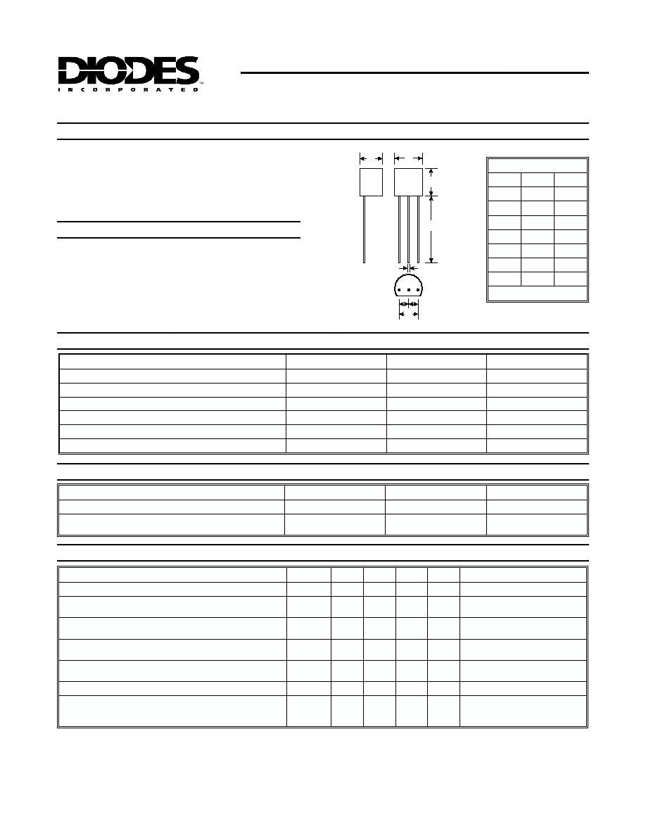
Case: TO-92, Plastic
∑
Leads: Solderable per MIL-STD-202,
Method 208
∑
Pin Connections: See Diagram
∑
Weight: 0.18 grams (approx.)
Mechanical Data
Maximum Ratings
@ T
A
= 25∞C unless otherwise specified
Notes:
1. Valid provided that leads are kept at ambient temperature at a distance of 2.0mm from case.
2. Pulse Test: Pulse width = 80µs, duty factor = 1%.
Characteristic
Symbol
Value
Unit
Drain-Source-Voltage
-V
DSS
240
V
Drain-Gate-Voltage
-V
DGS
200
V
Gate-Source-Voltage (pulsed) (Note 2)
V
GS
±20
V
Drain-Current (continuous)
-I
D
200
mA
Power Dissipation @T
C
= 25∞C (Note 1)
P
d
830
mW
Operating and Storage Temperature Range
T
j
, T
STG
≠55 to +150
∞C
∑
High Breakdown Voltage
∑
High Input Impedance
∑
Fast Switching Speed
∑
Low Drain-Source On-Resistance
∑
Specially Suited for Telephone Subsets
Inverse Diode
@ T
A
= 25∞C unless otherwise specified
Characteristic
Symbol
Value
Unit
Maximum Forward Current (continuous)
I
F
0.22
A
Forward Voltage Drop (Typical)
@ V
GS
= 0, I
F
= 0.75A, T
j
= 25∞C
V
F
0.85
V
D
S G D
H
H
BOTTOM
VIEW
E
A
B
C
G
TO-92
Dim
Min
Max
A
4.45
4.70
B
4.46
4.70
C
12.7
--
D
0.41
0.63
E
3.43
3.68
G
2.42
2.67
H
1.14
1.40
All Dimensions in mm
Characteristic
Symbol
Min
Typ
Max
Unit
Test Condition
Drain-Source Breakdown Voltage
-V
(BR)DSS
200
230
--
V
-I
D
= 100µA, V
GS
= 0
Gate-Body Leakage Current
-I
GSS
--
--
10
nA
-V
GS
= 15V, V
DS
= 0
Drain-Source Cutoff Current
-I
DSS
-I
DSX
--
--
1.0
25
µA
-V
DS
=130V, V
GS
= 0
-V
DS
= 10V, -V
GS
= 0.2V
Gate-Source Threshold Voltage
-V
GS(th)
--
2.8
4.0
V
V
GS
= V
DS
, -I
D
= 1.0mA
Drain-Source ON Resistance
r
DS(ON)
--
7.0
14
W
-V
GS
= 10V, -I
D
= 100 mA
Thermal Resistance Junction to Ambient
R
qJA
--
--
150
K/W
Note 1
Input Capacitance
Output Capacitance
Feedback Capacitance
C
iss
C
oss
C
rss
--
270
35
6.0
--
pF
-V
DS
= 20V, V
GS
= 0, f =1.0MHz
Electrical Characteristics
@ T
A
= 25∞C unless otherwise specified

D
S21901 Rev. E-3 2 of 2 BS208
0
10
-V , DRAIN-SOURCE VOLTAGE (V)
Fig. 3. Saturation Characteristics
DS
-I
,
DRAIN
ON-CURRENT
(mA)
D
0
100
200
300
400
500
See Note 2
-V
= 4.5V
GS
2
4
6
8
T = 25∞C
A
5.0
4.0
3.5
0
-V , GATE-SOURCE VOLTAGE (V)
Fig. 4. Drain-Source Current vs Gate-Source Voltage
GS
-I
DRAIN-SOURCE
CURRENT
(A)
DS,
0
0.2
0.4
0.6
0.8
1.0
2
4
T = 25∞C
A
(See Note 2)
6
8
10
-V
= 25V
DS
200
400
0
0
2
4
g
,
FOR
W
ARD
TRANSCONDUCT
ANCE
(mm)
fs
-V , GATE-SOURCE VOLTAGE (V)
Fig. 5. Transconductance vs Gate-Source Voltage
GS
-V
= 25V
DS
See Note 2
6
8
10
100
300
500
0
1000
-I , DRAIN CURRENT (mA)
Fig. 6. Transconductance vs. Drain Current
D
g
,
FOR
W
ARD
TRANSCONDUCT
ANCE
(mm)
fs
0
200
400
600
800
1000
500
See Note 2
-V
= 25V
DS
0
100
200
T , AMBIENT TEMPERATURE (∫C)
Fig. 1. Power Derating Curve
A
P
,
POWER
DISSIP
A
TION
(W)
d
0
0.2
0.4
0.6
0.8
1
(See Note 1)
0
20
100
0
0.4
0.8
1.2
1.6
2.0
40
60
80
T = 25∞C
A
See Note 2
-V
= 9V
GS
-V , DRAIN-SOURCE VOLTAGE (V)
Fig. 2, Output Characteristics
DS
-I
(ON),
DRAIN
ON-CURRENT
(A)
D
8
7
6
5
4
3.5
3