
DS30286 Rev. B-2
1 of 3
MBRD1035CTL
MBRD1035CTL
10A SURFACE MOUNT DUAL SCHOTTKY BARRIER RECTIFIER
Features
Single phase, half wave, 60Hz, resistive or inductive load.
For capacitive load, derate current by 20%.
∑
Case: DPAK Molded Plastic
∑
Terminals: Solderable per MIL-STD-202,
Method 208
∑
Polarity: See Diagram
∑
Marking: See Sheet 2
∑
Weight: 0.4 grams (approx.)
∑
Ordering Information: See Below
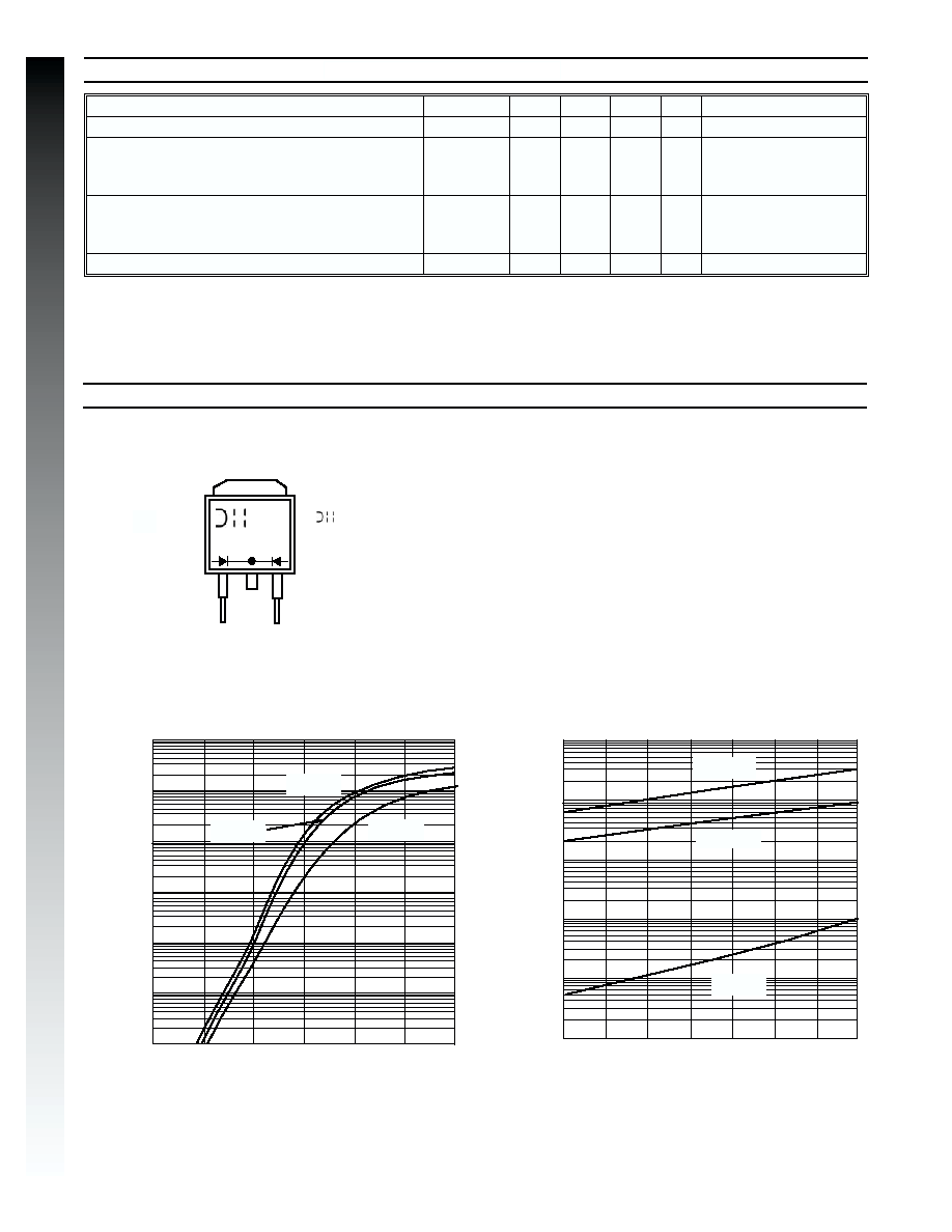
Mechanical Data
B
C
D
E
G
H
J
K
L
M
A
P
1
2
3
4
PIN 1
PIN 3
PIN 4, BOTTOMSIDE
HEAT SINK
Characteristic
Symbol
Value
Unit
Peak Repetitive Reverse Voltage
Working Peak Reverse Voltage
DC Blocking Voltage
V
RRM
V
RWM
V
R
35
V
RMS Reverse Voltage
V
R(RMS)
25
V
Average Rectified Output Current Per Leg
(See Figure 4) Per Package
I
O
5
10
A
Non-Repetitive Peak Forward Surge Current
8.3ms Single half sine-wave Superimposed on Rated Load
Per Package (JEDEC Method)
I
FSM
75
A
Typical Thermal Resistance Junction to Case Bottom Side Per Leg
(Note 1)
R
qJC
2.43
∞C/W
Voltage Rate of Change @ V
R
= 35V, T
j
= 25∞C
dv/dt
10,000
V/
ms
Operating Temperature Range
T
j
-55 to +125
∞C
Storage Temperature Range
T
STG
-55 to +125
∞C
∑
Guard Ring Die Construction for
Transient Protection
∑
Low Power Loss, High Efficiency
∑
High Surge Capability
∑
Very Low Forward Voltage Drop
∑
For Use in Low Voltage, High Frequency
Inverters, OR'ing, and Polarity Protection
Applications
∑
Plastic Material: UL Flammability
Classification Rating 94V-0
NEW
PRODUCT
Maximum Ratings
@ T
A
= 25
∞C unless otherwise specified
DPAK
Dim
Min
Max
A
6.3
6.7
B
æ
10
C
0.3
0.8
D
2.3 Nominal
E
2.1
2.5
G
0.4
0.6
H
1.2
1.6
J
5.3
5.7
K
0.5 Nominal
L
1.3
1.8
M
1.0
æ
P
5.1
5.5
All Dimensions in mm
Notes:
1. Device mounted on PC board with 14mm
2
(.013mm thick) copper pad areas.
Ordering Information
(Note 2)
Device
Packaging
Shipping
MBRD1035CTL-T
DPAK
2500/Tape & Reel
Notes:
2. For Packaging Details, go to our website at http://www.diodes.com/datasheets/ap02007.pdf.
MBRD1035CTL = Product type marking code
= Manufacturers' code marking
YWW = Date code marking
Y = Last digit of year ex: 2 for 2002
WW = Week code 01 to 52
YWW
MBRD
1035CTL
DS30286 Rev. B-2
2 of 3
MBRD1035CTL
Notes:
1. Device mounted on PC board with 14mm
2
(.013mm thick) copper pad areas.
2. For packaging details, go to our website at http://www.diodes.com/datasheets/ap02007.pdf.
3. Short duration pulse test used to minimize self-heating effect.
Characteristic
Symbol
Min
Typ
Max
Unit
Test Condition
Reverse Breakdown Voltage (Note 3)
V
(BR)R
35
æ
æ
V
I
R
= 500
mA
Forward Voltage (Note 3)
V
FM
æ
æ
æ
æ
æ
æ
æ
æ
0.47
0.41
0.56
0.55
V
I
F
= 5A, T
S
= 25
∞C
I
F
= 5A, T
S
= 100
∞C
I
F
= 10A, T
S
= 25
∞C
I
F
= 10A, T
S
= 100
∞C
Peak Reverse Current (Note 3)
I
RM
æ
æ
æ
æ
0.04
æ
æ
æ
2.0
30
200
5
mA
mA
mA
mA
V
R
= 35V, T
j
= 25∞C
V
R
= 35V, T
j
= 100∞C
V
R
= 17.5V, T
j
= 25∞C
V
R
= 17.5V, T
j
= 100∞C
Typical Junction Capacitance
C
j
æ
340
æ
pF
f = 1.0MHz, V
R
= 4.0V DC
Electrical Characteristics
@ T
A
= 25
∞C unless otherwise specified
NEW
PRODUCT
1
0.1
0.01
0.001
10
100
0
10
20
30
35
I
,
INST
ANT
ANE
O
US
REVERSE
CURRENT
(mA)
R
V , INSTANTANEOUS REVERSE VOLTAGE (V)
Fig. 2 Typical Reverse Characteristics (Per Element)
R
5
15
25
T = +25 C
j
∞
T = +125 C
j
∞
T = +100 C
j
∞
0
100
200
300
400
600
500
I
,
INST
ANT
ANE
O
US
F
O
R
W
ARD
CURRENT
(A)
F
V , INSTANTANEOUS FORWARD VOLTAGE (mV)
Fig. 1 Typical Forward Characteristics (Per Element)
F
10
1
0.1
0.01
0.001
0.0001
100
T = +25 C
j
∞
T = 125 C
j
∞
T = 100 C
j
∞
Marking Information
DS30286 Rev. B-2
3 of 3
MBRD1035CTL
NEW
PRODUCT
0
0.5
1.0
1.5
2.5
2.0
3.0
3.5
4.0
0
1
3
2
4
5
6
7
8
9
10
P
,
A
VERAGE
FOR
W
ARD
POWER
DISSIP
A
TION
(W
)
F(A
V)
I
, AVERAGE FORWARD CURRENT (A)
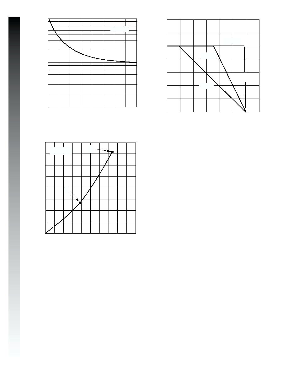
Fig. 5 Forward Power Dissipation (Per Element)
F(AV)
T = 125∞C
j
2
3
10
100
1000
0
15
10
25
30
35
20
40
C
,
JUNCTION
CAP
ACIT
ANCE
(pF)
j
V , REVERSE VOLTAGE (V)
Fig. 3 Typical Junction Capacitance vs.
Reverse Voltage (Per Element)
R
5
f = 1MHz
0
1
2
4
3
5
6
7
-25
0
25
50
75
100
125
150
I
,
A
VERAGE
F
O
R
W
ARD
CURRENT
(A)
F(A
V)
T , AMBIENT TEMPERATURE (∞C)
Fig. 4 DC Forward Current Derating (Per Element)
A
Note 1
Note 2
Note 3
Notes: 1. T
A
= T
SOLDERING POINT
, R
qJC
= 2.43
∞C/W, R
qCA
= 0
∞C/W.
2. Device mounted on GETEK substrate, 2"x2", 2 oz. copper, double-sided, cathode pad dimensions 0.75" x 1.0", anode pad
dimensions 0.25" x 1.0". R
qJA
in range of 15-30∞C/W.
3. Device mounted on FR-4 substrate, 2"x2", 2 oz. copper, single-sided, pad layout as per Diodes Inc. suggested pad layout
document AP02001 which can be found on our website at http://www.diodes.com/datasheets/ap02001.pdf. R
qJA
in range of
60-75∞C/W.