DS30163 Rev. B-1
1 of 2
MMST4124
MMST4124
NPN SMALL SIGNAL SURFACE MOUNT TRANSISTOR
∑
Epitaxial Planar Die Construction
∑
Complementary PNP Type Available
(MMST4126)
∑
Ideal for Medium Power Amplification and
Switching
∑
Ultra-Small Surface Mount Package
Characteristic
Symbol
MMST4124
Unit
Collector-Base Voltage
V
CBO
30
V
Collector-Emitter Voltage
V
CEO
25
V
Emitter-Base Voltage
V
EBO
5.0
V
Collector Current - Continuous (Note 1)
I
C
200
mA
Power Dissipation (Note 1)
P
d
200
mW
Thermal Resistance, Junction to Ambient (Note 1)
R
qJA
625
K/W
Operating and Storage and Temperature Range
T
j
, T
STG
-55 to +150
∞C
Features
Maximum Ratings
@ T
A
= 25
∞C unless otherwise specified
A
E
J
L
M
B C
H
G
D
K
TOP VIEW
C
E
B
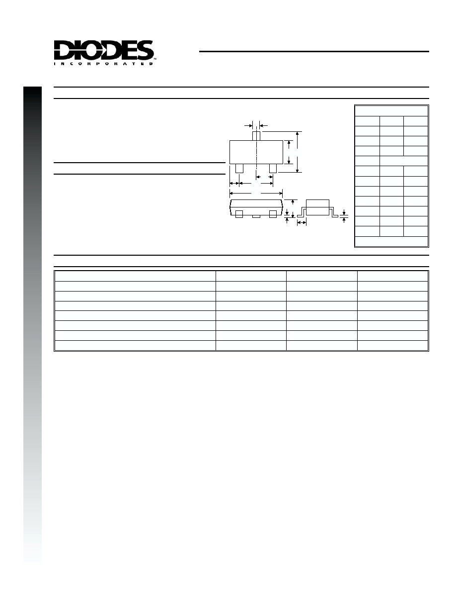
Mechanical Data
∑
Case: SOT-323, Molded Plastic
∑
Terminals: Solderable per MIL-STD-202,
Method 208
∑
Terminal Connections: See Diagram
∑
Marking: K1B
∑
Weight: 0.006 grams (approx.)
Notes:
1. Valid provided that terminals are kept at ambient temperature.
2. Pulse test: Pulse width
£ 300ms, duty cycle £ 2%.
SOT-323
Dim
Min
Max
A
0.30
0.40
B
1.15
1.35
C
2.00
2.20
D
0.65 Nominal
E
0.30
0.40
G
1.20
1.40
H
1.80
2.20
J
0.0
0.10
K
0.90
1.00
L
0.25
0.40
M
0.10
0.25
All Dimensions in mm
NEW
PRODUCT

DS30163 Rev. B-1
2 of 2
MMST4124
NEW
PRODUCT
Electrical Characteristics
@ T
A
= 25
∞C unless otherwise specified
Characteristic
Symbol
Min
Max
Unit
Test Condition
OFF CHARACTERISTICS (Note 2)
Collector-Base Breakdown Voltage
V
(BR)CBO
30
æ
V
I
C
= 10
mA, I
E
= 0
Collector-Emitter Breakdown Voltage
V
(BR)CEO
25
æ
V
I
C
= 1.0mA, I
B
= 0
Emitter-Base Breakdown Voltage
V
(BR)EBO
5.0
6.0
V
I
E
= 10
mA, I
C
= 0
Collector Cutoff Current
I
CBO
æ
50
nA
V
CB
= 20V, I
E
= 0V
Emitter Cutoff Current
I
EBO
æ
50
nA
V
EB
= 3.0V, I
C
= 0V
ON CHARACTERISTICS (Note 2)
DC Current Gain
h
FE
120
60
360
æ
æ
I
C
= 2.0mA, V
CE
= 1.0V
I
C
= 50mA, V
CE
= 1.0V
Collector-Emitter Saturation Voltage
V
CE(SAT)
æ
0.30
V
I
C
= 50mA, I
B
= 5.0mA
Base- Emitter Saturation Voltage
V
BE(SAT)
æ
0.95
V
I
C
= 50mA, I
B
= 5.0mA
SMALL SIGNAL CHARACTERISTICS
Output Capacitance
C
obo
æ
4.0
pF
V
CB
= 5.0V, f = 1.0MHz, I
E
= 0
Input Capacitance
C
ibo
æ
8.0
pF
V
EB
= 0.5V, f = 1.0MHz, I
C
= 0
Small Signal Current Gain
h
fe
120
480
æ
V
CE
= 1.0V, I
C
= 2.0mA,
f = 1.0kHz
Current Gain-Bandwidth Product
f
T
300
æ
MHz
V
CE
= 20V, I
C
= 10mA,
f = 100MHz
Notes:
1. Valid provided that terminals are kept at ambient temperature.
2. Pulse test: Pulse width
£ 300ms, duty cycle £ 2%.