D
S23006 Rev. F-2 1 of 2 SD830 - SD860
∑
High Current Capability and Low Forward Drop
∑
High Surge Capacity
∑
Guard Ring for Transient Protection
∑
Low Power Loss, High Efficiency
∑
Plastic Package has UL Flammability
Classification 94V-0
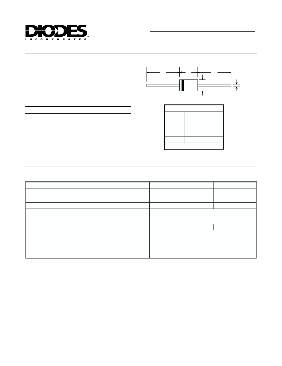
Mechanical Data
∑
Case: DO-201AD, Molded Plastic
∑
Leads: Solderable per MIL-STD-202,
Method 208
∑
Polarity: Cathode band
∑
Approx. Weight: 1.1 grams
∑
Mounting Position: Any
Single phase, half wave, 60Hz, resistive or inductive load.
For capacitive load, derate current by 20%.
Maximum Ratings and Electrical Characteristics
@ TA = 25∞C unless otherwise specified
Notes:
1. Thermal Resistance from Junction to Lead Vertical PC Board Mounting, 9.5mm Lead Length.
2. Measured at 1.0MHz and applied reverse voltage of 4.0V.
SD830 - SD860
8.0A SCHOTTKY BARRIER RECTIFIERS
Features
Characteristic
Symbol
SD830
SD840
SD845
SD860
Unit
Peak Repetitive Reverse Voltage
Working Peak Reverse Voltage
DC Blocking Voltage
V
RRM
V
RWM
V
R
30
40
45
60
V
RMS Reverse Voltage
V
R(RMS
)
21
28
31.5
42
V
Maximum Average Forward Rectified Current
T
L
=90∞C
I
O
8.0
A
Peak Forward Surge current 8.3ms half sine-wave
superimposed on rated load (JEDEC Method)
I
FSM
175
A
Maximum Forward Voltage at 8.0A
V
F
0.55
0.70
V
Maximum Average Reverse Current at
T
A
= 25∞C
Peak Reverse Voltage
T
A
=100∞C
I
R
1.0
50
mA
Typical Thermal Resistance (Note 1)
R
qJL
30
K/W
Typical Junction Capacitance (Note 2)
C
j
550
pF
Operating and Storage Temperature Range
T
j,
T
STG
-65 to +150
∞C
DO-201AD
Dim
Min
Max
A
25.40
--
B
7.20
9.50
C
1.20
1.30
D
4.80
5.30
All Dimensions in mm
A
A
B
C
D
D
S23006 Rev. F-2 2 of 2 SD830 - SD860
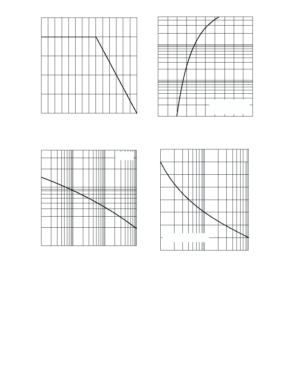
0
2
4
6
8
10
20
40
60
80
100 120 140
I
,
A
VERAGE
RECTIFIED
CURRENT
(A)
O
T , LEAD TEMPERATURE (∫C)
Fig. 1 Forward Current Derating Curve
L
0
25
50
75
100
125
150
175
1.0
10
100
I
,
PEAK
FOWRARD
SURGE
CURRENT
(A)
FSM
NUMBER OF CYCLES AT 60Hz
Fig. 4 Max Non-Repetitive Peak Fwd Surge Current
200
8.3 ms Single Half Sine-Wave
JEDEC Method
100
1000
4000
0.1
1.0
10
100
C
,
CAP
ACIT
ANCE
(pF)
j
V , REVERSE VOLTAGE (VOLTS)
Fig. 3 Typical Junction Capacitance
R
TJ = 25∫C
f = 1MHz
0.1
1.0
10
50
0.1
0.3
0.5
0.7
0.9
1.1
I
,
INST
ANT
ANEOUS
FOR
W
ARD
CURRENT
(A)
F
V , INSTANTANEOUS FWD VOLTAGE (V)
Fig. 2 Typical Forward Characteristics
F
TJ = 25∫C
Pulse Width = 300ms
1% Duty Cycle