 | –≠–ª–µ–∫—Ç—Ä–æ–Ω–Ω—ã–π –∫–æ–º–ø–æ–Ω–µ–Ω—Ç: DS2906SZ | –°–∫–∞—á–∞—Ç—å:  PDF PDF  ZIP ZIP |
1/7
www.dynexsemi.com
DS2906SZ
FEATURES
s
Double Side Cooling
s
High Surge Capability
APPLICATIONS
s
Rectification
s
Freewheel Diode
s
DC Motor Control
s
Power Supplies
s
Welding
s
Battery Chargers
VOLTAGE RATINGS
ORDERING INFORMATION
When ordering, select the required part number shown in the
Voltage Ratings selection table, e.g.:
DS2906SZ39
Note: Please use the complete part number when ordering
and quote this number in any future correspondance relating
to your order.
KEY PARAMETERS
V
RRM
4000V
I
F(AV)
5651A
I
FSM
83000A
DS2906SZ
Rectifier Diode
Replaces July 2000 version, DS4186-4.1
DS4186-5.0 October 2001
4000
3900
3800
3700
3600
3500
DS2906SZ40
DS2906SZ39
DS2906SZ38
DS2906SZ37
DS2906SZ36
DS2906SZ35
Conditions
V
RSM
= V
RRM
+ 100V
Lower voltage grades available
Type Number
Repetitive Peak
Reverse Voltage
V
RRM
V
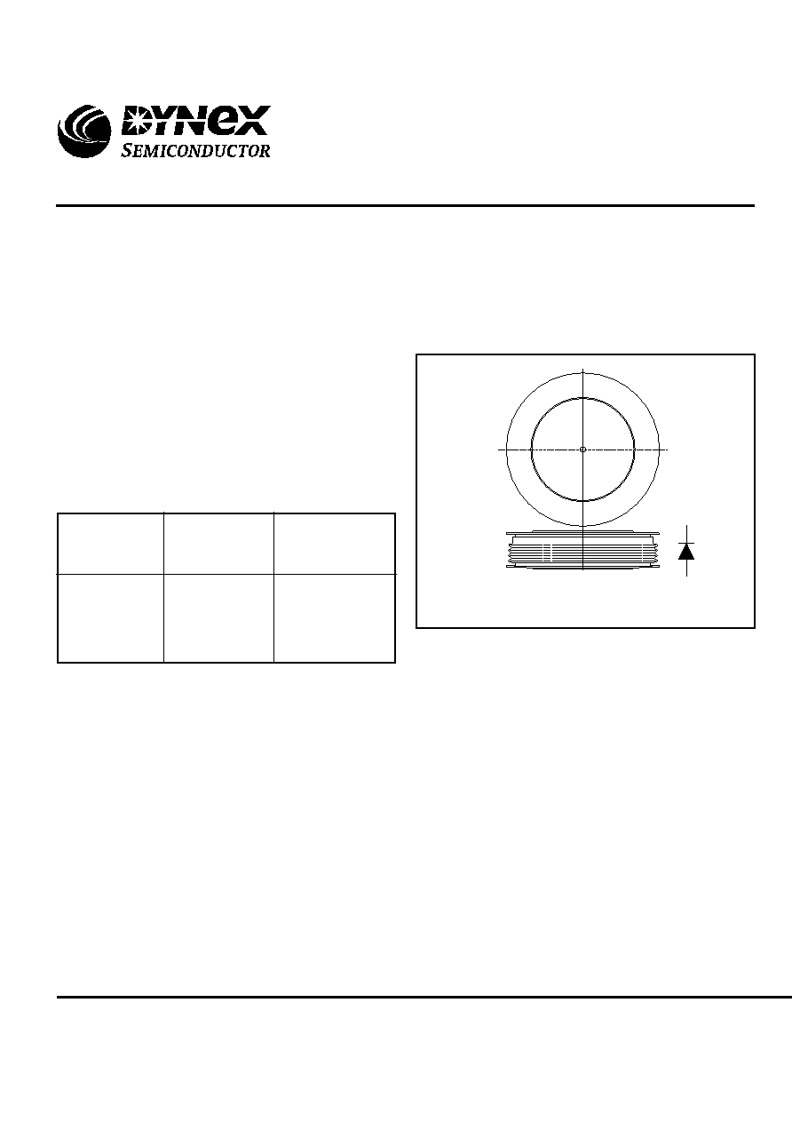
Outline type code: Z
See Package Details for further information.
Fig. 1 Package outline
2/7
www.dynexsemi.com
DS2906SZ
Symbol
Parameter
Conditions
Double Side Cooled
I
F(AV)
Mean forward current
I
F(RMS)
RMS value
I
F
Continuous (direct) forward current
Single Side Cooled (Anode side)
I
F(AV)
Mean forward current
I
F(RMS)
RMS value
I
F
Continuous (direct) forward current
Units
Max.
Half wave resistive load
4350
A
-
6830
A
-
6160
A
Half wave resistive load
2795
A
-
4390
A
-
3640
A
CURRENT RATINGS
T
case
= 75
o
C unless otherwise stated
Symbol
Parameter
Conditions
Double Side Cooled
I
F(AV)
Mean forward current
I
F(RMS)
RMS value
I
F
Continuous (direct) forward current
Single Side Cooled (Anode side)
I
F(AV)
Mean forward current
I
F(RMS)
RMS value
I
F
Continuous (direct) forward current
Units
Max.
Half wave resistive load
5651
A
-
8877
A
-
8208
A
Half wave resistive load
3707
A
-
5821
A
-
4976
A
T
case
= 100
o
C unless otherwise stated
3/7
www.dynexsemi.com
DS2906SZ
SURGE RATINGS
Conditions
10ms half sine; T
case
= 150
o
C
V
R
= 50% V
RRM
- 1/4 sine
10ms half sine; T
case
= 150
o
C
V
R
= 0
Max.
Units
Symbol
Parameter
I
FSM
Surge (non-repetitive) forward current
I
2
t
I
2
t for fusing
I
FSM
Surge (non-repetitive) forward current
I
2
t
I
2
t for fusing
A
2
s
83
kA
22.0 x 10
6
A
2
s
66.5
kA
THERMAL AND MECHANICAL DATA
dc
Conditions
Min.
Max.
Units
o
C/W
-
0.013
Anode dc
Clamping force 83.0kN
with mounting compound
Thermal resistance - case to heatsink
R
th(c-h)
0.001
Double side
-
150
o
C
T
vj
Virtual junction temperature
T
stg
Storage temperature range
Reverse (blocking)
Single side
-
Thermal resistance - junction to case
R
th(j-c)
Single side cooled
Symbol
Parameter
Clamping force
75.0
91.0
kN
≠55
150
o
C
Forward (conducting)
160
o
C
-
0.002
o
C/W
o
C/W
Cathode dc
-
0.013
o
C/W
Double side cooled
-
0.0065
o
C/W
CHARACTERISTICS
Forward voltage
Peak reverse current
Parameter
Symbol
V
FM
I
RM
At V
RRM
, T
case
= 150
o
C
-
400
mA
-
1.06
V
At 3000A peak, T
case
= 25
o
C
Conditions
Min.
Max.
Units
34.5 x 10
6
-
-
At T
vj
= 150∞C
-
V
TO
Threshold voltage
r
T
Slope resistance
0.0763
m
At T
vj
= 150∞C
-
0.78
V
4/7
www.dynexsemi.com
DS2906SZ
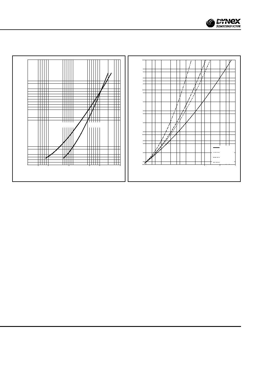
CURVES
0
1000
2000
3000
4000
5000
6000
7000
8000
0.5
0.6
0.7
0.8
0.9
1
1.1
1.2
1.3
1.4
Instantaneous forward voltage, V
F
- (V)
Instantaneous f
orw
ard current, I
F
- (A)
T
j
= 150∞C
T
j
= 25∞C
Fig. 2 Maximum (limit) forward characteristics
Fig. 3 Power loss curves
0
1000
2000
3000
4000
5000
6000
7000
0
1000
2000
3000
4000
5000
6000
Mean on-state current, I
T(AV)
- (A)
Mean po
w
er dissipation - (W)
dc
1/2 wave
3 phase
6 phase
V
FM
Equation:-
V
FM
= A + Bln (I
F
) + C.I
F
+D.
I
F
Where
A = ≠0.01591
B = 0.113682
C = 8.04 x 10
≠5
D = ≠0.00284
these values are valid for T
j
= 125∞C for I
F
500A to 7000A

5/7
www.dynexsemi.com
DS2906SZ
10
1
0.1
0.01
0.001
Time - (s)
0.1
0.01
0.001
0.0001
Thermal impedance - (
∞
C/W)
Double side cooled
Anode side cooled
100
Conduction
d.c.
Halfwave
3 phase 120∞
6 phase 60∞
Effective thermal resistance
Junction to case ∞C/W
Double side
0.0065
0.0072
0.0073
0.0076
Single side
0.013
0.0137
0.0138
0.0141
Fig. 6 Maximum (limit) transient thermal impedance -
junction to case - (∞C/W)
Fig. 4 Stored charge
Fig. 5 Reverse recovery current
0
2000
4000
6000
8000
10000
12000
14000
16000
0
1
2
3
4
5
6
7
8
Rate of decay of forward current, dI
f
/dt - (A/
µ
s)
Stored charge
,
Qs - (
µ
C)
0
50
100
150
200
250
300
350
0
1
2
3
4
5
6
7
8
Rate of decay of forward current, dI
f
/dt - (A/
µ
s)
Re
v
e
rse reco
v
e
r
y
current, I
RR
- (A)