 | –≠–ª–µ–∫—Ç—Ä–æ–Ω–Ω—ã–π –∫–æ–º–ø–æ–Ω–µ–Ω—Ç: DSF8025SE | –°–∫–∞—á–∞—Ç—å:  PDF PDF  ZIP ZIP |
DSF8025SE
1/8
APPLICATIONS
s
Induction Heating
s
A.C. Motor Drives
s
Inverters And Choppers
s
Welding
s
High Frequency Rectification
s
UPS
FEATURES
s
Double side cooling
s
High surge capability
s
Low recovery charge
VOLTAGE RATINGS
KEY PARAMETERS
V
RRM
2500V
I
F(AV)
650A
I
FSM
7500A
Q
r
540
µ
C
t
rr
5.0
µ
s
CURRENT RATINGS
Symbol
Parameter
Conditions
Double Side Cooled
I
F(AV)
Mean forward current
I
F(RMS)
RMS value
I
F
Continuous (direct) forward current
Single Side Cooled (Anode side)
I
F(AV)
Mean forward current
I
F(RMS)
RMS value
I
F
Continuous (direct) forward current
Units
Max.
Half wave resistive load, T
case
= 65
o
C
650
A
T
case
= 65
o
C
1020
A
T
case
= 65
o
C
785
A
Half wave resistive load, T
case
= 65
o
C
385
A
T
case
= 65
o
C
604
A
T
case
= 65
o
C
465
A
2500
2400
2300
2200
2100
2000
DSF8025SE25
DSF8025SE24
DSF8025SE23
DSF8025SE22
DSF8025SE21
DSF8025SE20
Conditions
V
RSM
= V
RRM
+ 100V
Lower voltage grades available.
Type Number
Repetitive Peak
Reverse Voltage
V
RRM
V
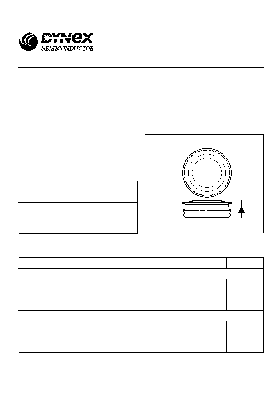
Outline type code: E
See Package Details for further information.
DSF8025SE
Fast Recovery Diode
Advance Information
Replaces March 1998 version, DS4146-4.4
DS4146-5.0 January 2000

DSF8025SE
2/8
SURGE RATINGS
Conditions
Max.
Units
7.5
kA
281 x 10
3
A
2
s
I
2
t for fusing
I
2
t
Surge (non-repetitive) forward current
I
FSM
Parameter
Symbol
10ms half sine; with 0% V
RRM,
T
j
= 150
o
C
6.0
kA
180 x 10
3
A
2
s
I
2
t for fusing
I
2
t
Surge (non-repetitive) forward current
I
FSM
10ms half sine; with 50% V
RRM,
T
j
= 150
o
C
THERMAL AND MECHANICAL DATA
dc
Conditions
Max.
Units
o
C/W
-
0.094
Anode dc
Clamping force 8.0kN
with mounting compound
Thermal resistance - case to heatsink
R
th(c-h)
0.018
Double side
-
Single side
Thermal resistance - junction to case
R
th(j-c)
Single side cooled
Symbol
Parameter
-
0.036
o
C/W
o
C/W
Cathode dc
-
0.094
o
C/W
Double side cooled
-
0.047
o
C/W
T
stg
Storage temperature range
-55
175
o
C
kN
9.0
7.0
Clamping force
-
T
vj
Virtual junction temperature
On-state (conducting)
-
150
o
C
Min.
CHARACTERISTICS
t
rr
50
Symbol
Typ.
Units
Parameter
V
FM
Forward voltage
I
RRM
Peak reverse current
Reverse recovery time
Q
RA1
Recovered charge (50% chord)
I
RM
Reverse recovery current
K
Soft factor
V
TO
Threshold voltage
r
T
Slope resistance
V
FRM
Forward recovery voltage
di/dt = 1000A/
µ
s, T
j
= 125
o
C
70
-
V
At T
vj
= 150
o
C
-
0.8
m
At T
vj
= 150
o
C
-
1.48
V
1.8
-
-
-
235
A
-
540
µ
C
-
5.0
µ
s
At V
RRM
, T
case
= 150
o
C
-
mA
At 1000A peak, T
case
= 25
o
C
-
2.3
V
Conditions
Max.
I
F
= 1000A, di
RR
/dt = 100A/
µ
s
T
case
= 150
o
C, V
R
= 100V
DSF8025SE
3/8
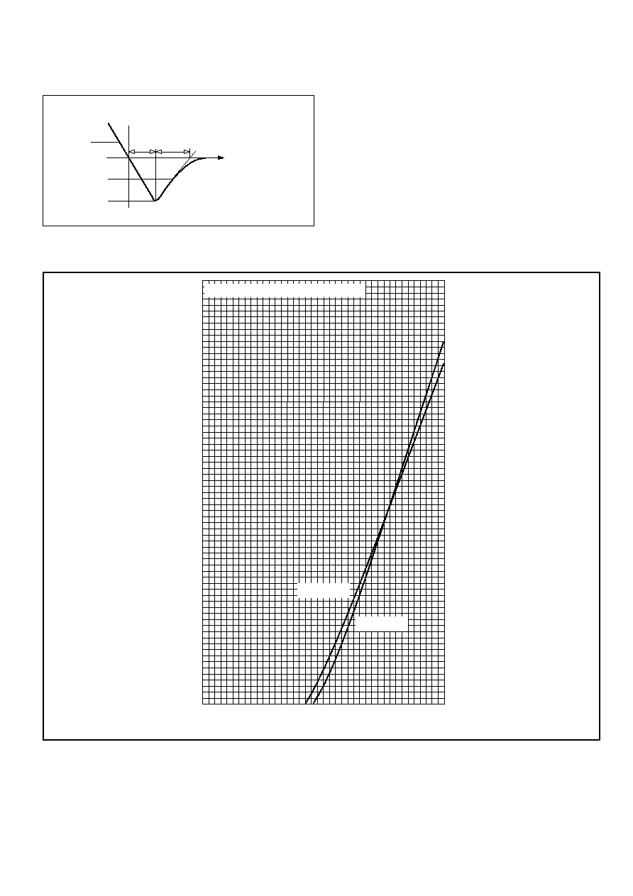
CURVES
500
1000
1500
2000
2500
3000
Instantaneous forward current I
F
- (A)
0
1.0
2.0
3.0
4.0
Instantaneous forward voltage V
F
- (V)
Measured under pulse conditions
T
j
= 150∞C
T
j
= 25∞C
3500
4000
DEFINITION OF K FACTOR AND Q
RA1
0.5x I
RR
I
RR
dI
R
/dt
t
1
t
2
Q
RA1
= 0.5x I
RR
(t
1
+ t
2
)
k = t
1
/t
2
Fig. 1 Maximum (limit) forward characteristics

DSF8025SE
4/8
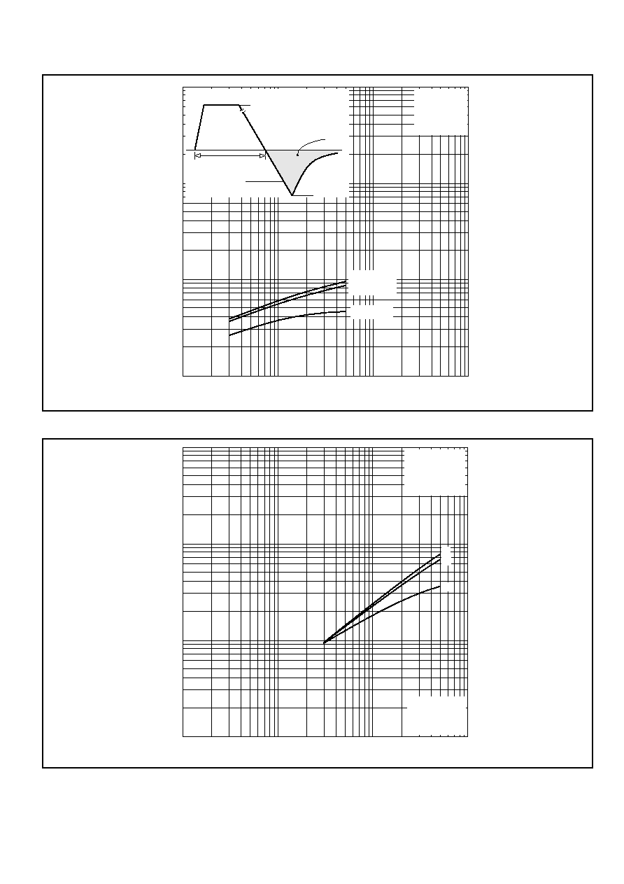
0
100
200
300
400
500
Instantaneous forward current I
F
- (A)
1.00
1.25
1.50
1.75
2.00
Instantaneous forward voltage V
F
- (V)
Measured under pulse conditions
T
j
= 150∞C
T
j
= 25∞C
0
50
100
150
200
250
Transient forward votage V
FP
- (V)
0
500
1000
1500
2000
Rate of rise of forward current dI
F
/dt - (A/
µ
s)
T
j
= 125∞C limit
T
j
= 25∞C limit
Current
waveform
Voltage
waveform
V
FR
y
x
di =
y
dt
x
Fig. 2 Maximum (limit) forward characteristics
Fig. 3 Transient forward voltage vs rate of rise of forward current
DSF8025SE
5/8
10
100
1000
10000
Rate of rise of reverse current dI
R
/dt - (A/
µ
s)
1000
100
10000
100000
Reverse recovered charge Q
S
- (
µ
C)
I
F
= 2000A
I
F
= 1000A
I
F
= 200A
I
RR
QS
t
p
= 1ms
I
F
dI
R
/dt
Q
S
=
Conditions:
T
j
= 150∞C,
V
R
= 100V
50
µ
s
0
1
10
100
1000
Rate of rise of reverse current dI
R
/dt - (A/
µ
s)
100
10
1000
10000
Reverse recovery current I
RR
- (A)
Conditions:
T
j
= 150∞C,
V
R
= 100V
A
B
C
A: I
F
= 2000A
B: I
F
= 1000A
C: I
F
= 200A
Fig. 4 Recovered charge
Fig. 5 Typical reverse recovery current vs rate of fall of forward current